

Page 1
®
VN920SP
SINGLE CHANNEL HIGH SIDE SOLID STATE RELAY
TYPE R
DS(on)
I
OUT
V
CC
VN920SP 15mΩ 30 A 36 V
■ CMOS COMPATIBLE INPUT
■ PROPORTIONAL LOAD CURRENT SENSE
■ SHORTED LOAD PROTECTION
■ UNDERVOLTAGE AND OVERVOLTAGE
SHUTDOWN
■ OVERVOLTAGE CLAMP
■ THERMAL SHUTDOWN
■ CURRENT LIMITATION
■ PROTECTION AGAINST LOSS OF GROUND
AND LOSS V
■ VERY L OW ST AND -BY P OWER DISSI PATIO N
■ REVERSE BA TTERY PROTECTION (*)
CC
DESCRIPTION
The VN920SP is a mono lithic d evice designe d in
STMicroelectronics VIPower M0-3 Technology,
intended for driving any kind of load with one side
connected to ground. Active VCC pin voltage
clamp protects the device against low energy
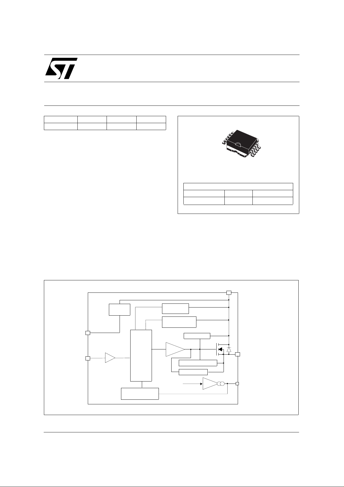
BLOCK DIAGRAM
10
1
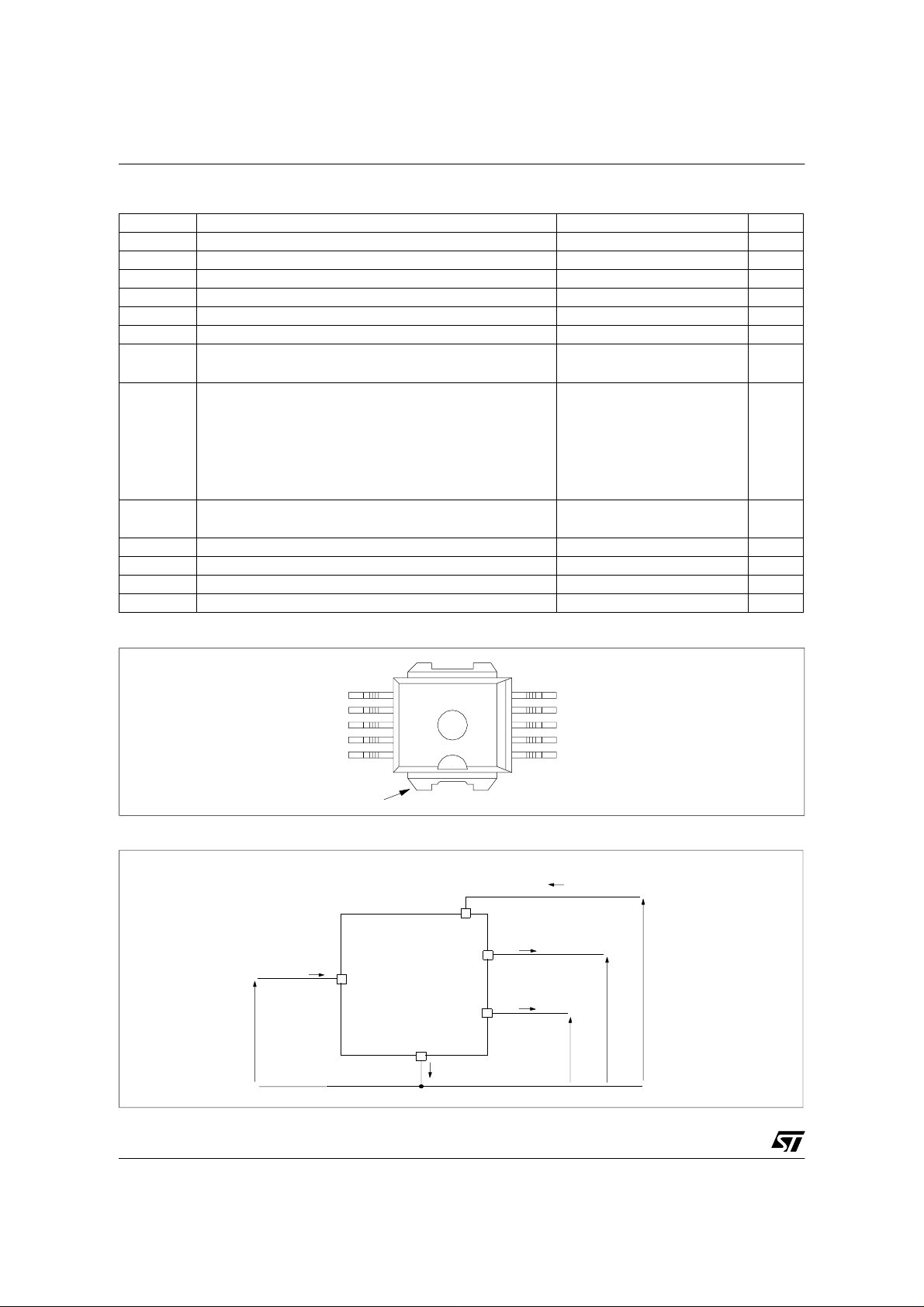
PowerSO-10
ORDER CODES
PACKAGE TUBE T&R
PowerSO-10 VN920SP VN920SP13TR
spikes (see ISO7637 transient compatibility
table). Active current limitation combined with
thermal shutdown and automatic restart protect
the device against overload. The device
integrates an analog current sens e output which
delivers a current proportional to the load current.
Device autom atically turns off in case of gro und
pin disconnection.
V
CC
OVERVO LTAGE
DETECTION
UNDERVOLTAGE
DETECTION
DRIVER
CURRENT LIMITER
I
Power CLAMP
OUTPUT
VDS LIMITER
OUT CURRENT
K
SENSE
GND
INPUT
(*) See application schematic at page 8
V
CC
CLAMP
OVERTEMPERATURE
DETECTION
LOGIC
October 20 02 1/16
1
Page 2
VN920SP
ABSOLUTE MAXIMUM RATI NG
Symbol Parameter Value Unit
tot
DC Supply Voltage 41 V
Reverse DC Supply Voltage - 0.3 V
CC
DC Reverse Ground Pin Current - 200 mA
DC Output Current Internally Limited A
Reverse DC Output Current - 40 A
DC Input Current +/- 10 mA
Current Sense Maximum Voltag e -3
+15
Electros tatic Discharge
(Human Body Model: R=1.5KΩ; C=100pF)
- INPUT
- CURRENT SENSE
- OUTPU T
- V
CC
Maximum Switching Energy
(L=0.25m H; R
=0Ω; V
L
=13.5V ; T
bat
=150ºC ; IL=45A)
jstart
4000
2000
5000
5000
362 mJ
Powe r Dissip a tion TC≤25°C 96.1 W
Junction Operati ng Temperature Internally limi ted °C
j
Case Operating Temperature - 40 to 150 °C
c
Storage Temperature - 55 to 150 °C
V
- V
- I
GND
I
OUT
- I
OUT
I
V
CSENSE
V
ESD
E
MAX
P
T
T
T
STG
CC
IN
V
V
V
V
V
V
CONNECTION DIAGRAM (TOP VIEW)
GROUND
INPUT
C.SENSE
N.C.
N.C.
6
7
8
9
10
V
CC
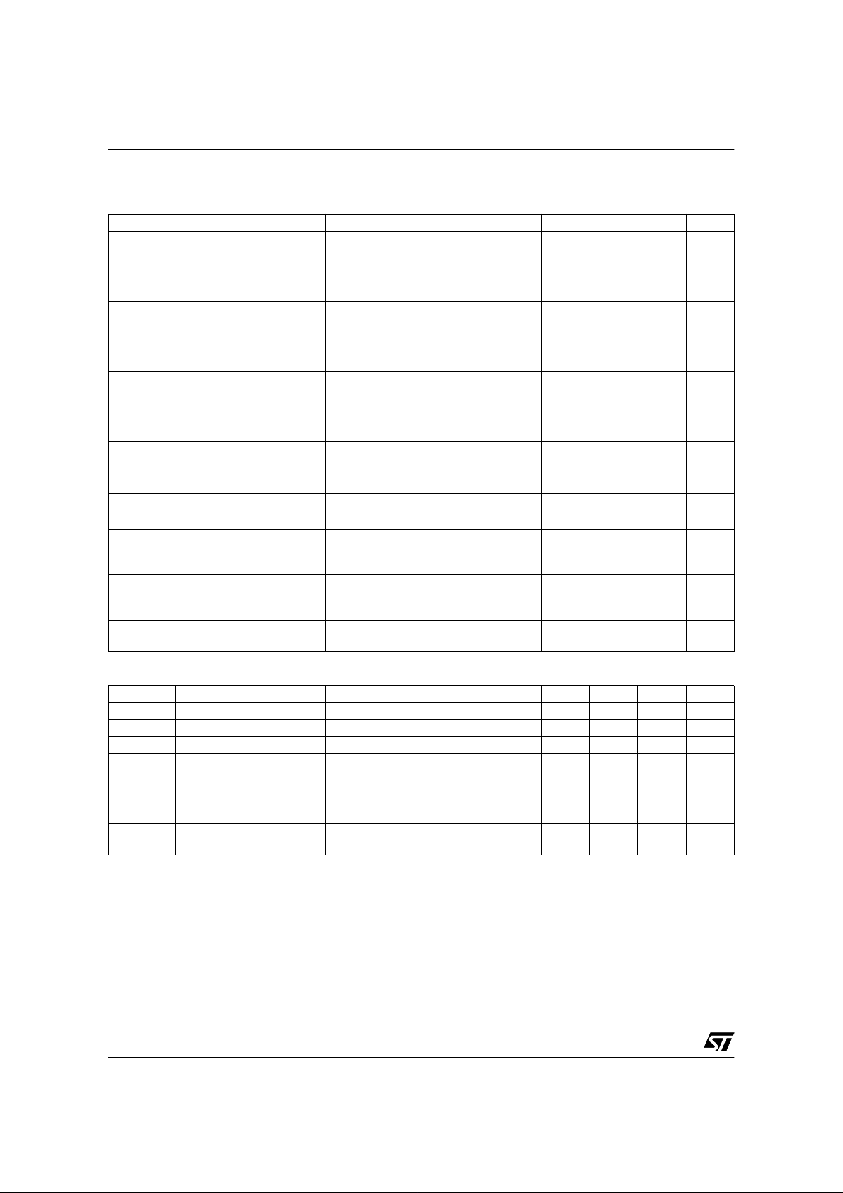
CURRENT AND VOLTAGE CONVENTIONS
I
IN
V
IN
INPUT
CURRENT SENSE
11
GND
V
CC
OUTPUT
I
GND
5
4
3
2
1
I
OUT
I
SENSE
V
SENSE
OUTPUT
OUTPUT
N.C.
OUTPUT
OUTPUT
I
S
V
OUT
V
CC
2/16
1
Page 3
VN920SP
THERMAL DATA
Symbol Parameter Va lu e Unit
R
thj-case
R
thj-amb
(*) When mounted on a standard si ngle-sided FR-4 board with 0.5c m2 of Cu (at leas t 35µ m t hick) .
Thermal R esistanc e Junctio n-case
Thermal R esistanc e Junctio n-ambient
Max
Max
ELECTRICAL CHARACTERISTICS (8V<VCC<36V; -40°C<Tj<150°C unless otherwise specified)
POWER
Symbol Parameter Test Conditions Min Typ Max Unit
V
CC
V
USD
V
OV
R
ON
V
clamp
I
I
L(off1)
I
L(off2)
I
L(off3)
I
L(off4)
Oper ating Supp ly Vo ltage 5.5 13 36 V
Undervolt age Shut- down 3 4 5.5 V
Overvolt age Shut-down 36 V
I
=10A; Tj =25°C
On State Resistance
OUT
I
=10A
OUT
I
=3A; VCC=6V
OUT
Clam p Vo ltage ICC=20mA (See note 1) 41 48 55 V
Supply Current
S
Off State Output Curr ent VIN=V
Off State Output Curr ent VIN=0V; V
Off State Output Curr ent VIN=V
Off State Output Curr ent VIN=V
Off State; V
Off State; V
On State; V
R
=3.9KΩ
SENSE
OUT
OUT
OUT
=13V; VIN=V
CC
=13V; Tj=25°C; VIN=V
CC
=13V; VIN=5V; I
CC
=0V 0 50 µA
=3.5V -75 0 µA
OUT
=0V; Vcc=13V; Tj =125°C 5 µA
=0V; Vcc=13V; Tj =25°C 3 µA
OUT
=0V
OUT
=0;
OUT
=0V
1.3 °C/W
51.3 (*) °C/W
15
30
50
10
10
25
20
5
mΩ
mΩ
mΩ
µA
µA
mA
SWITCHING (VCC=13V)
Symbol Parameter Test Conditions Min Typ Max Unit
t
d(on)
t
d(off)
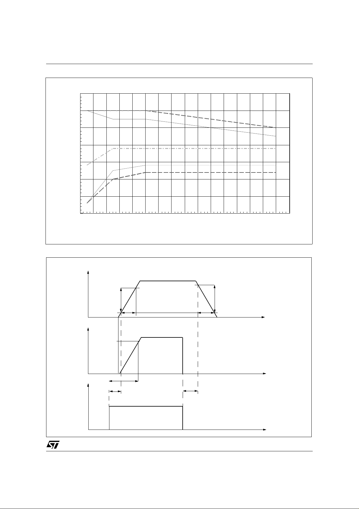
Turn-on Delay Time RL=1.3Ω (see figure 2) 50 µs
Turn-off Delay Time RL=1.3Ω (see figure 2) 50 µs
See
/dt
dV
OUT
Turn-on Voltage Slope RL=1.3Ω (see figure 2)
(on)
relative
diagram
See
/dt
dV
OUT
Turn-off Voltag e Slope RL=1.3Ω (see figure 2)
(off)
relative
diagram
LOGIC INPUT
Symbol Parameter Test Conditio ns Mi n Typ Max Unit
V
I
V
I
IH
V
I(hyst)
V
ICL
Note 1: V
Input Low Level 1.25 V
IL
Low Level Input Current VIN=1.25V 1 µA
IL
Input High Level 3.25 V
IH
High Level Input Current VIN=3.25V 10 µA
Input Hyst eresis Vo lt age 0.5 V
I
=1mA
Input Clamp Voltage
and VOV are correlated. Typical difference is 5V.
clamp
IN
I
IN
=-1mA
66.8
-0.7
8V
V/µs
V/µs
V
3/16
1
Page 4
VN920SP
ELECTRICAL CHARACTERISTICS (continued)
CURRENT SENSE (9V≤ VCC≤16V) (See Fig. 1)
Symbol Parameter Test Conditions Min Typ Max Unit
I
K
I
1
OUT/ISENSE
dK1/K1Current Se nse Ratio Drif t
K
I
2
OUT/ISENSE
dK2/K2Current Se nse Ratio Drif t
K
I
3
OUT/ISENSE
dK3/K3Current Se nse Ratio Drif t
I
SENSEO
V
SENSE
Analog Sense Leakage
Current
Max Analog Sense Output
Voltage
Sense Voltage in
V
SENSEH
Overtemperature
conditions
Analog sense output
R
VSENSEH
t
DSENSE
impedance in
overtemperature condition
Current sense dela y
response
=1A; V
OUT
T
= -40°C...150°C
j
=1A; V
I
OUT
T
= -40°C...+150°C
j
I
=10A; V
OUT
T
=25°C... 150°C
j
=10A; V
I
OUT
T
=-40°C.. .+150°C
j
I
=30A; V
OUT
T
=25°C... 150°C
j
=30A; V
I
OUT
T
=-40°C.. .+150°C
j
V
=6...16V; I
CC
T
=-40°C.. .+150°C
j
=5.5V; I
V
CC
V
>8V; I
CC
VCC=13V; R
VCC=13V; Tj>T
to 90% I
SENSE
=0.5V;
SENSE
SENSE
SENSE
SENSE
SENSE
SENSE
OUT
OUT
SENSE
=0.5V;
=4V; Tj=-40°C
=4V;
=4V; Tj=-40°C
=4V;
=0A;V
OUT
=5A; R
=10A; R
SENSE
SENSE
SENSE
=0V;
=10KΩ
=10KΩ
=3.9KΩ 5.5 V
; Output Open 400 Ω
TSD
3300 4400 6000
-10 +10 %
4200
4400
4900
4900
6000
5750
-8 +8 %
4200
4400
4900
4900
5500
5250
-6 +6 %
010µA
2
4
(see note 2) 500 µs
V
V
PROTECTIONS
Symbol Parameter Test Conditions Min Typ Max Unit
T
TSD
T
T
hyst
I
lim
V
demag
V
ON
Note 2: current sense signal delay after posi tive input slope
Note: Sense pin doesn’t have to be left floating.
Shut-down Temperat ure 150 17 5 200 °C
Reset Temperature 135 °C
R
Thermal Hysteres is 7 15 °C
DC Short Circuit Current
Turn-off Output Clamp
Voltage
Output Voltage Drop
Limitation
=13V
V
CC
5V<V
I
I
<36V
CC
=2A; VIN=0V; L= 6m H VCC-41 VCC-48 VCC-55 V
OUT
=1A; Tj=-40°C....+150°C 50 mV
OUT
30 45 75
75
4/16
2
A
A
1
Page 5
VN920SP
Figure 1: I
OUT/ISENSE
I
OUT/ISENSE
versus I
OUT
6500
6000
max.Tj=-40°C
5500
max.Tj=25...150°C
5000
min.Tj=25...150°C
4500
4000
3500
3000
02468101214161820222426283032
I
(A)
OUT
typi cal val ue
min.Tj=-40°C
Figure 2: Switching Characteristics (Resistive load RL=1.3Ω)
V
OUT
80%
dV
/dt
OUT
(on)
10%
t
d(off)
I
SENSE
INPUT
t
d(on)
90%
t
DSENSE
t
r
90%
t
f
dV
OUT
/dt
(off)
t
t
t
5/16
1
Page 6

VN920SP
TRUTH TABLE
CONDITIONS INPUT OUTPUT SENSE
Normal op eration
Overtemperature
Undervoltage
Overvoltage
L
H
L
H
L
H
L
H
L
Short circuit to GND
H
H
Short circuit to V
CC
L
H
Negative output voltage cl amp L L 0
ELECTRICAL TRANS IENT REQUIREMENTS
L
H
Nominal
L
L
V
L
L
L
L
L
L
L
(T
(T
j<TTSD
j>TTSD
H
H
< Nominal
0
0
SENSEH
0
0
0
0
0
) 0
) V
SENSEH
0
ISO T/R 7637/1
Test Pulse
I II III IV Delays and
TEST LEVELS
Impedance
1 -25 V -50 V -75 V -100 V 2 ms 10 Ω
2 +25 V +50 V +75 V +100 V 0.2 ms 10 Ω
3a -25 V -50 V -100 V -150 V 0.1 µs 50 Ω
3b +25 V +50 V +75 V +100 V 0.1 µs 50 Ω
4 -4 V -5 V -6 V -7 V 100 ms, 0.01
5 +26.5 V +46.5 V +66.5 V +86.5 V 400 ms, 2
ISO T/R 7637/1
Test Pulse
I II III IV
TEST LEVELS RESULTS
Ω
1CCCC
2CCCC
3aCCCC
3bCCCC
4CCCC
5CEEE
CLASS CONTENTS
C All functi ons of the device are performed as designed after exposure to disturbance.
E One or more funct ions of the device is not perform ed as designed after exposure to disturbance
and cann ot be returned to proper oper ation without replacing the device.
Ω
6/16
1
Page 7

Figure 3: W aveforms
INPUT
LOAD CURRENT
SENSE
V
CC
INPUT
LOAD CURREN T
SENSE
V
CC
INPUT
LOAD CURRENT
SENSE
V
USD
V
VCC > V
VN920SP
NORMAL OPERATION
UNDERVOLTAGE
V
USDhyst
OVERVOLT AGE
OV
V
USD
OVhyst
INPUT
LOAD CURRENT
LOAD VOLTAGE
SENSE
INPUT
LOAD VOLTAGE
LOAD CURRENT
SENSE
T
j
INPUT
LOAD CURRENT
SENSE
SHORT TO GROUND
SHORT TO V
<Nominal
T
TSD
T
R
OVERTEMPERATURE
CC
<Nominal
I
SENSE
=
V
SENSEH
R
SENSE
7/16
1
1
Page 8

VN920SP
APPLICATION SCHEMATIC
+5V
R
prot
INPUT
R
µ
C
prot
R
CURRENT SENSE
SENSE
GND PROTECTION NETWORK AGAINST
REVERSE BATTERY
Soluti on 1: Resistor in the ground line (R
can be us ed with any t ype of load .
The fo llow ing is a n indication on how to dimensi on the
resistor.
R
GND
1) R
2) R
where -I
be found in the absolute maximum rating section of the
≤ 600mV / (I
GND
≥ (−VCC) / (-I
GND
is the DC re vers e grou nd pi n cu rren t an d can
GND
S(on)ma x
)
GND
).
device’s datasheet.
Power Dissipation in R
battery situations) is:
= (-VCC)2/R
P
D
GND
(when VCC<0: during reverse
GND
This resistor can be shared amongst several different
HSD. Please note tha t th e va l u e of this resis t o r sh ould be
calcul ated with form ula (1) wher e I
sum of the maximum on-state currents of the different
S(on)max
devices.
Please note that if the microprocessor ground is not
common with the device ground then the R
produce a shift (I
and the status output values. This shift will vary
S(on)max
* R
) in the input thresholds
GND
depend ing on how many devi ces are ON in the c ase of
several high side drivers sharing t he same R
If the calculated power dissipation leads to a large resistor
or several devices hav e to share the sa me resisto r then
the ST suggests to utiliz e Solu tio n 2 (se e below ).
Solution 2:
A resistor (R
D
GND
A diode (D
=1kΩ) sh ould b e insert ed in paral lel to
GND
if the device will be driving an induc tive load.
) in the gr ound line.
GND
only). This
GND
becomes t he
GND
.
GND
will
V
CC
D
OUTPUT
GND
R
GND
GND
D
GND
V
This small signal diode can be safely shared amongst
several different HSD. Also in this case, the presence of
j
the ground network wi ll produce a shift (
600mV) in t he
input threshold and the status output values if the
microprocessor ground is not common with the device
ground. This shift will not vary if more than one HSD
shares the same diode/resistor net work.
LOAD DUMP PROTECTION
Dld is necessary (Voltage Transient Suppressor) if the
load dump peak voltage exceeds VCC max DC rating. The
same applies if the device will be subject to transients on
the VCC line that are grea ter tha n the ones sh own in the
ISO T/R 7637/1 table.
C I/Os PROTECTION:
µ
If a ground protection network is used and negative
transients are present on the VCC line, th e con trol p ins will
be pulled negative. ST suggests to insert a resistor (R
in lin e to prevent the µC I/Os pins to latch-up.
The value of these resistors is a compromise between the
leakage c urrent of µC an d the current required by the
HSD I/Os ( Input le vels comp atibilit y) wi th the lat ch-up li mit
of µC I/Os.
≤ R
-V
CCpeak/Ilatchup
Calculation exam ple:
CCpeak
prot
= - 100V an d I
≤ 65kΩ.
prot
For V
5kΩ ≤ R
Recommended R
≤ (V
prot
OHµC-VIH-VGND
≥ 20mA; V
latchup
value is 10kΩ.
) / I
OHµC
ld
IHmax
≥ 4.5V
prot
)
8/16
11
1
Page 9

VN920SP
Off State Output Current
IL(off1) (u A)
9
8
7
6
5
4
3
2
1
0
-50 -25 0 25 50 75 100 125 150 175
Tc (°C)
Input Clamp Voltage
Vicl (V)
8
7.8
7.6
7.4
7.2
7
6.8
6.6
6.4
6.2
6
Iin=1mA
-50 -25 0 25 50 75 100 125 150 175
Tc (°C)
High Level Input Current
Iih (uA)
5
4.5
3.5
2.5
1.5
0.5
Vin=3.25V
4
3
2
1
0
-50 -25 0 25 50 75 100 125 150 175
Input High Level
Vih (V)
3.6
3.4
3.2
3
2.8
2.6
2.4
2.2
2
-50 -25 0 25 50 75 100 125 150 175
Input Hysteresis VoltageInput Low Level
Tc (°C)
Tc (°C)
Vil (V)
2.6
2.4
2.2
2
1.8
1.6
1.4
1.2
1
-50 -25 0 25 50 75 100 125 150 175
Tc (°C)
1
Vhyst (V)
1.5
1.4
1.3
1.2
1.1
1
0.9
0.8
0.7
0.6
0.5
-50 -25 0 25 50 75 100 125 150 175
Tc (°C)
9/16
111
Page 10

VN920SP
Overvoltage Shutdown
I
LIM
Vs T
case
Vov (V)
50
48
46
44
42
40
38
36
34
32
30
-50 -25 0 25 50 75 100 125 150 175
Ilim (A)
100
90
80
70
60
50
40
30
20
10
0
Vcc=13 V
-50 -25 0 25 50 75 100 125 150 175
Tc (°C)
Turn-on Voltage Slope Turn-off Voltage Slope
dVout/dt(on) (V/ms)
700
650
600
550
500
450
400
350
300
250
-50 -25 0 25 50 75 100 125 150 175
Vcc=13V
Rl=1.3Ohm
Tc (ºC)
dVout/dt(off) (V/ms)
550
500
450
400
350
300
250
200
150
100
50
Vcc=13V
Rl=1.3Ohm
0
-50 -25 0 25 50 75 100 125 150 175
Tc (°C)
Tc (°C)
On State Resistance Vs T
case
Ron (mOhm)
30
27.5
25
22.5
20
17.5
15
12.5
10
7.5
5
Iout=10A
Vcc=8V; 36V
-25 0 25 50 75 100 125 150 175
Tc (ºC)
10/16
11
On State Resistance Vs V
Ron (mOhm)
30
27.5
25
22.5
20
17.5
15
12.5
10
7.5
5
2.5
0
5 10152025303540
IOUT=10A
Vcc (V)
CC
Tc= 150ºC
Tc= 25ºC
Tc= - 40ºC
Page 11

Maximum turn off current versus load inductance
LMAX (A)
I
100
A
B
C
10
VN920SP
1
0.01 0.1 1 10 100
A = Single Pulse at T
B= Repetitive pulse at T
C= Repetitive Pulse at T
Conditions:
VCC=13.5V
Values are generated with RL=0Ω
In case of repetitive pulses, T
the temperature specified above for curves B and C.
VIN, I
L
=150ºC
Jstart
=100ºC
Jstart
=125ºC
Jstart
jstart
Demagnetization
(at beginning of each demagnetization) of every pulse must not exceed
L(mH)
Demagnetization
Demagnetization
t
11/16
Page 12

VN920SP
PowerSO-10™ PC Board
PowerSO-10™ THERMAL DATA
R
thj-amb
Layout condition of Rth and Zth measurements (PCB FR 4 area= 58mm x 58mm, PCB thi ckness=2mm,
Cu thickness=35µm, Copper areas: from minimum pad lay-out to 8cm
Vs PCB copper area in open box free air condition
2
).
RTHj_amb (°C/W)
55
Tj-Tamb=50°C
50
45
40
35
12/16
30
0246810
PCB Cu heatsink area (cm^2)
Page 13

PowerSO-10 Thermal Impedance Junction Ambient Single Pulse
ZTH (°C /W)
VN920SP
100
10
1
0.1
0.01
0.0001 0.001 0.01 0.1 1 10 100 1000
Time (s)
Thermal fitting model of a single channel HSD
in PowerSO-10
Pulse calculation formula
Z
THδ
where
RTHδ Z
δ tpT⁄=
THtp
2
0.5 cm
2
6 cm
1 δ–()+⋅=
Tj
Pd
C1
R1 R2
Thermal Parameter
Area/island (cm2)0.56
R1 (°C/W) 0.02
C2
C3
R3
C4
R4
C5
R5
C6
R6
R2 (°C/W) 0.1
R3( °C/W) 0.2
R4 (°C/W) 0.8
R5 (°C/W) 12
T_amb
R6 (°C/W) 37 22
C1 (W.s/°C) 0.0015
C2 (W.s/°C) 7.00E-03
C3 (W.s/°C) 0.015
C4 (W.s/°C) 0.3
C5 (W.s/°C) 0.75
C6 (W.s/°C) 3 5
13/16
Page 14

VN920SP
PowerSO-10™ MECHANICAL DATA
DIM.
MIN. TYP MAX. MIN. TYP. MAX.
mm. inch
A 3.35 3.65 0.132 0.144
A (*) 3.4 3.6 0.134 0.142
A1 0.00 0.10 0.000 0.004
B 0.40 0.60 0.016 0.024
B (*) 0.37 0.53 0.014 0.021
C 0.35 0.55 0.013 0.022
C (*) 0.23 0.32 0.009 0.0126
D 9.40 9.60 0.370 0.378
D1 7.40 7.60 0.291 0.300
E 9.30 9.50 0.366 0.374
E2 7.20 7.60 0.283 300
E2 (*) 7.30 7.50 0.287 0.295
E4 5.90 6.10 0.232 0.240
E4 (*) 5.90 6.30 0.232 0.248
e 1.27 0.050
F 1.25 1.35 0.049 0.053
F (*) 1.20 1.40 0.047 0.055
H 13.80 14.40 0.543 0.567
H (*) 13.85 14.35 0.545 0.565
h 0.50 0.002
L 1.20 1.80 0.047 0.070
L (*) 0.80 1.10 0.031 0.043
α 0º 8º 0º 8º
α (*) 2º 8º 2º 8º
(*) Muar only POA P013P
14/16
HE
h
A
F
A1
10
1
eB
0.25
D
= =
D1
= =
E2
DETAIL "A"
DETA IL "A"
B
0.10 A
SEATING
PLANE
A
C
α
B
E4
SEATING
PLANE
A1
L
P095A
Page 15

VN920SP
PowerSO-10™ SUGGESTED PAD LAYOUT
14.6 - 14.9
10.8 - 11
6.30
0.67 - 0.73
1
2
3
9.5
4
5
10
0.54 - 0.6
9
8
7
1.27
6
TAPE AND REEL SHIPMENT (suffix “1 3TR”)
TUBE SHIPMENT (no suffix)
C
A
B
A
All dimensi ons ar e in mm.
Base Q.ty Bulk Q.ty Tube length (± 0.5) A B C (± 0.1)
Casablanca 50 10 00 532 10.4 16.4 0.8
Muar 50 1000 532 4.9 1 7.2 0.8
MUARCASABLANCA
B
REEL DIMENSIONS
Base Q.ty 600
Bulk Q.ty 600
A (max) 330
B (min) 1.5
C (± 0.2) 13
F 20.2
G (+ 2 / -0) 24.4
N (min) 60
T (max) 30.4
C
TAPE DIMENSIONS
According to Electronic Industries Association
(EIA) Standard 481 rev. A, Feb 1986
Tape width W 24
Tape Hole Spacing P0 (± 0.1) 4
Component Spacing P 24
Hole Diameter D (± 0.1/-0) 1.5
Hole Diameter D1 (min) 1.5
Hole Position F (± 0.05) 11.5
Compartm ent Depth K (max) 6.5
Hole Spacing P1 (± 0.1) 2
All dimensions are in mm.
Top
cover
tape
End
500mm min
All dimensions are in mm.
Empty components pockets
saled with cover tape.
User direction of feed
500mm min
Start
No componentsNo components Components
15/16
1
1
Page 16

VN920SP
Information furnished is believed to be ac c ur ate and reliab le. However, STMicroelectronics as s um es no responsibility for the consequences
of use of such information nor for any infringement of patents or other rights of third parties which may results from its use. No license is
granted by implication or oth er wise under any patent or patent rights of STMicroelectronics . Specificatio ns m entioned in this publication are
subject to c hange without notice. This publication s upersedes an d r eplaces all information p r ev iously supplied. STMicroelectronic s pr oducts
are not authorized for use as critical components in life support devices or systems without express written approval of STMicroelectronics.
Australia - Brazil - Canada - China - Finland - France - Germany - Hong Kong - India - Israel - Italy - Japan - M alaysia -
Malta - Moro c c o - S ingapore - Spai n - Sw eden - Switzerla nd - United Kingdom - U.S.A.
The ST logo is a trademark of STM ic r oelectronics
2002 STMicroelectronics - Printed in ITALY- All Rights Reserved.
STMicroelectronics GROUP OF COMPANIES
http://www.st.com
16/16
1
 Loading...