

Page 1
Features
Type R
VN772KP-E 125 mΩ
1. Total resistance of one side in bridge configuration
2. Typical current limitation value
DS(on)
(1)
I
OUT
9A
(2)
VCC
36 V
VN772KP-E
Quad smart power solid state relay
for complete H-bridge configurations
■ ECOPACK
■ Automotive Grade: compliance with AEC
®
: lead free and RoHS compliant
guidelines
■ Suited as low voltage bridge
■ Linear current limitation
■ Very low standby power dissipation
■ Short circuit protected
■ Status flag diagnostic (open drain)
■ Integrated clamping circuits
■ Undervoltage protection
■ ESD protection
Description
The VN772KP-E is a device formed by three
monolithic chips housed in a standard SO-28
package: a double high side and two low side
switches. Both the double high side and low side
switches are made using STMicroelectronics
VIPower™ M0-3 Technology.
Table 1. Device summary
SO-28
This device is suitable to drive a DC motor in a
bridge configuration as well as to be used as a
quad switch for any low voltage application.
The dual high side switches have built-in thermal
shutdown to protect the chips from over
temperature and current limiter blocks to protect
the device from short circuit. Status output is
provided to indicate open load in off and on-state
and over temperature.
The low side switches are two OMNIFET II types
(fully auto protected Power MOSFET in
VIPower™ technology). They have built-in
thermal shutdown, linear current limitation and
overvoltage clamping. Fault feedback for thermal
intervention can be detected by monitoring the
voltage at the input pin.
Order codes
Package
Tube Tape and reel
SO-28 VN772KP-E VN772KPTR-E
July 2011 Doc ID 022022 Rev 1 1/33
www.st.com
1
Page 2

Contents VN772KP-E
Contents
1 Block diagram and pin description . . . . . . . . . . . . . . . . . . . . . . . . . . . . . 6
2 Electrical specifications . . . . . . . . . . . . . . . . . . . . . . . . . . . . . . . . . . . . . . 8
2.1 Thermal data . . . . . . . . . . . . . . . . . . . . . . . . . . . . . . . . . . . . . . . . . . . . . . . 8
2.2 Absolute maximum ratings . . . . . . . . . . . . . . . . . . . . . . . . . . . . . . . . . . . . . 8
2.3 Electrical characteristics for dual high side switch . . . . . . . . . . . . . . . . . . . 9
2.4 Electrical characteristics for low side switches . . . . . . . . . . . . . . . . . . . . 11
2.5 Dual high-side switch timing data . . . . . . . . . . . . . . . . . . . . . . . . . . . . . . 13
2.6 Electrical characterization for dual high side switch . . . . . . . . . . . . . . . . . 15
2.7 Electrical characterization for low side switches . . . . . . . . . . . . . . . . . . . . 18
3 Application recommendations . . . . . . . . . . . . . . . . . . . . . . . . . . . . . . . . 22
4 Thermal data . . . . . . . . . . . . . . . . . . . . . . . . . . . . . . . . . . . . . . . . . . . . . . 25
4.1 SO-28 thermal data . . . . . . . . . . . . . . . . . . . . . . . . . . . . . . . . . . . . . . . . . 25
4.2 Thermal calculation in clockwise and anti-clockwise operation in steady
state mode . . . . . . . . . . . . . . . . . . . . . . . . . . . . . . . . . . . . . . . . . . . . . . . . 26
4.2.1 Thermal resistances definition . . . . . . . . . . . . . . . . . . . . . . . . . . . . . . . 26
4.2.2 Thermal calculation in transient mode . . . . . . . . . . . . . . . . . . . . . . . . . 26
4.2.3 Single pulse thermal impedance definition . . . . . . . . . . . . . . . . . . . . . . 26
4.2.4 Pulse calculation formula . . . . . . . . . . . . . . . . . . . . . . . . . . . . . . . . . . . . 26
5 Package mechanical data . . . . . . . . . . . . . . . . . . . . . . . . . . . . . . . . . . . 29
5.1 ECOPACK® package . . . . . . . . . . . . . . . . . . . . . . . . . . . . . . . . . . . . . . . . 29
5.2 SO-28 mechanical data . . . . . . . . . . . . . . . . . . . . . . . . . . . . . . . . . . . . . . 29
5.3 SO-28 tube shipment . . . . . . . . . . . . . . . . . . . . . . . . . . . . . . . . . . . . . . . 31
5.4 Tape and reel shipment . . . . . . . . . . . . . . . . . . . . . . . . . . . . . . . . . . . . . . 31
6 Revision history . . . . . . . . . . . . . . . . . . . . . . . . . . . . . . . . . . . . . . . . . . . 32
2/33 Doc ID 022022 Rev 1
Page 3

VN772KP-E List of tables
List of tables
Table 1. Device summary . . . . . . . . . . . . . . . . . . . . . . . . . . . . . . . . . . . . . . . . . . . . . . . . . . . . . . . . . . 1
Table 2. Pin definition and function. . . . . . . . . . . . . . . . . . . . . . . . . . . . . . . . . . . . . . . . . . . . . . . . . . . 7
Table 3. Thermal data. . . . . . . . . . . . . . . . . . . . . . . . . . . . . . . . . . . . . . . . . . . . . . . . . . . . . . . . . . . . . 8
Table 4. Dual high side switch . . . . . . . . . . . . . . . . . . . . . . . . . . . . . . . . . . . . . . . . . . . . . . . . . . . . . . 8
Table 5. Low side switch. . . . . . . . . . . . . . . . . . . . . . . . . . . . . . . . . . . . . . . . . . . . . . . . . . . . . . . . . . . 8
Table 6. Power outputs (per each channel) . . . . . . . . . . . . . . . . . . . . . . . . . . . . . . . . . . . . . . . . . . . . 9
Table 7. Switching (per each channel) (V
Table 8. Logic input (per each channel) . . . . . . . . . . . . . . . . . . . . . . . . . . . . . . . . . . . . . . . . . . . . . . 10
Table 9. Status pin (per each channel) . . . . . . . . . . . . . . . . . . . . . . . . . . . . . . . . . . . . . . . . . . . . . . . 10
Table 10. Protections (per each channel) . . . . . . . . . . . . . . . . . . . . . . . . . . . . . . . . . . . . . . . . . . . . . . 10
Table 11. Openload detection (per each channel) . . . . . . . . . . . . . . . . . . . . . . . . . . . . . . . . . . . . . . . 11
Table 12. Off-state . . . . . . . . . . . . . . . . . . . . . . . . . . . . . . . . . . . . . . . . . . . . . . . . . . . . . . . . . . . . . . . 11
Table 13. On-state . . . . . . . . . . . . . . . . . . . . . . . . . . . . . . . . . . . . . . . . . . . . . . . . . . . . . . . . . . . . . . . 12
Table 14. Dynamic . . . . . . . . . . . . . . . . . . . . . . . . . . . . . . . . . . . . . . . . . . . . . . . . . . . . . . . . . . . . . . . 12
Table 15. Switching . . . . . . . . . . . . . . . . . . . . . . . . . . . . . . . . . . . . . . . . . . . . . . . . . . . . . . . . . . . . . . 12
Table 16. Source drain diode . . . . . . . . . . . . . . . . . . . . . . . . . . . . . . . . . . . . . . . . . . . . . . . . . . . . . . . 12
Table 17. Protections . . . . . . . . . . . . . . . . . . . . . . . . . . . . . . . . . . . . . . . . . . . . . . . . . . . . . . . . . . . . . 13
Table 18. Truth table. . . . . . . . . . . . . . . . . . . . . . . . . . . . . . . . . . . . . . . . . . . . . . . . . . . . . . . . . . . . . . 13
Table 19. Thermal calculation in clockwise and anti-clockwise operation in steady state mode . . . . 26
Table 20. Thermal parameters . . . . . . . . . . . . . . . . . . . . . . . . . . . . . . . . . . . . . . . . . . . . . . . . . . . . . . 28
Table 21. SO-28 mechanical data . . . . . . . . . . . . . . . . . . . . . . . . . . . . . . . . . . . . . . . . . . . . . . . . . . . 30
Table 22. Document revision history . . . . . . . . . . . . . . . . . . . . . . . . . . . . . . . . . . . . . . . . . . . . . . . . . 32
= 13V) . . . . . . . . . . . . . . . . . . . . . . . . . . . . . . . . . . . . . 10
CC
Doc ID 022022 Rev 1 3/33
Page 4

List of figures VN772KP-E
List of figures
Figure 1. Block diagram . . . . . . . . . . . . . . . . . . . . . . . . . . . . . . . . . . . . . . . . . . . . . . . . . . . . . . . . . . . . 6
Figure 2. Connection diagram . . . . . . . . . . . . . . . . . . . . . . . . . . . . . . . . . . . . . . . . . . . . . . . . . . . . . . . 7
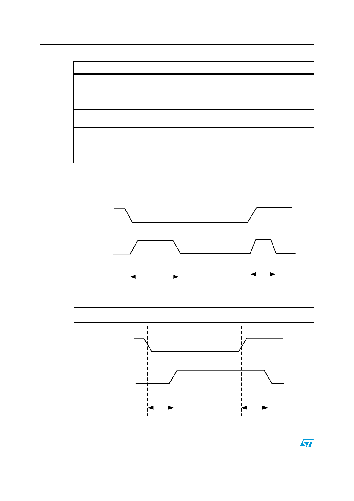
Figure 3. Switching time waveforms . . . . . . . . . . . . . . . . . . . . . . . . . . . . . . . . . . . . . . . . . . . . . . . . . 13
Figure 4. Open-load status timing (with external pull-up) . . . . . . . . . . . . . . . . . . . . . . . . . . . . . . . . . 14
Figure 5. Over temperature status timing . . . . . . . . . . . . . . . . . . . . . . . . . . . . . . . . . . . . . . . . . . . . . 14
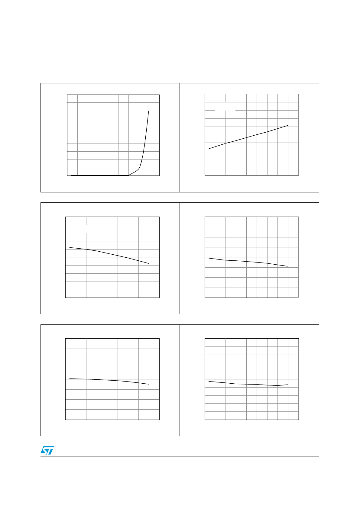
Figure 6. Off-state output current. . . . . . . . . . . . . . . . . . . . . . . . . . . . . . . . . . . . . . . . . . . . . . . . . . . . 15
Figure 7. Input clamp voltage. . . . . . . . . . . . . . . . . . . . . . . . . . . . . . . . . . . . . . . . . . . . . . . . . . . . . . . 15
Figure 8. High level input current . . . . . . . . . . . . . . . . . . . . . . . . . . . . . . . . . . . . . . . . . . . . . . . . . . . . 15
Figure 9. Input high level voltage . . . . . . . . . . . . . . . . . . . . . . . . . . . . . . . . . . . . . . . . . . . . . . . . . . . . 15
Figure 10. Input low level voltage . . . . . . . . . . . . . . . . . . . . . . . . . . . . . . . . . . . . . . . . . . . . . . . . . . . . 15
Figure 11. Input hysteresis voltage . . . . . . . . . . . . . . . . . . . . . . . . . . . . . . . . . . . . . . . . . . . . . . . . . . . 15
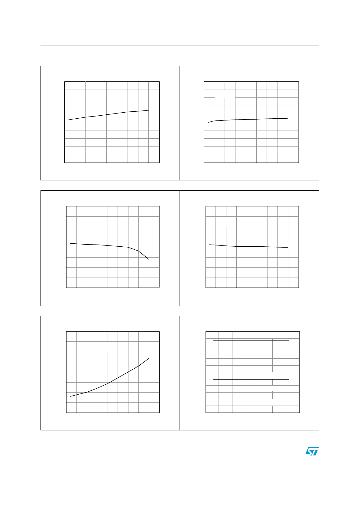
Figure 12. Overvoltage shutdown . . . . . . . . . . . . . . . . . . . . . . . . . . . . . . . . . . . . . . . . . . . . . . . . . . . . 16
Figure 13. I
Figure 14. Turn-on voltage slope . . . . . . . . . . . . . . . . . . . . . . . . . . . . . . . . . . . . . . . . . . . . . . . . . . . . . 16
Figure 15. Turn-off voltage slope . . . . . . . . . . . . . . . . . . . . . . . . . . . . . . . . . . . . . . . . . . . . . . . . . . . . . 16
Figure 16. On-state resistance vs T
Figure 17. On-state resistance vs V
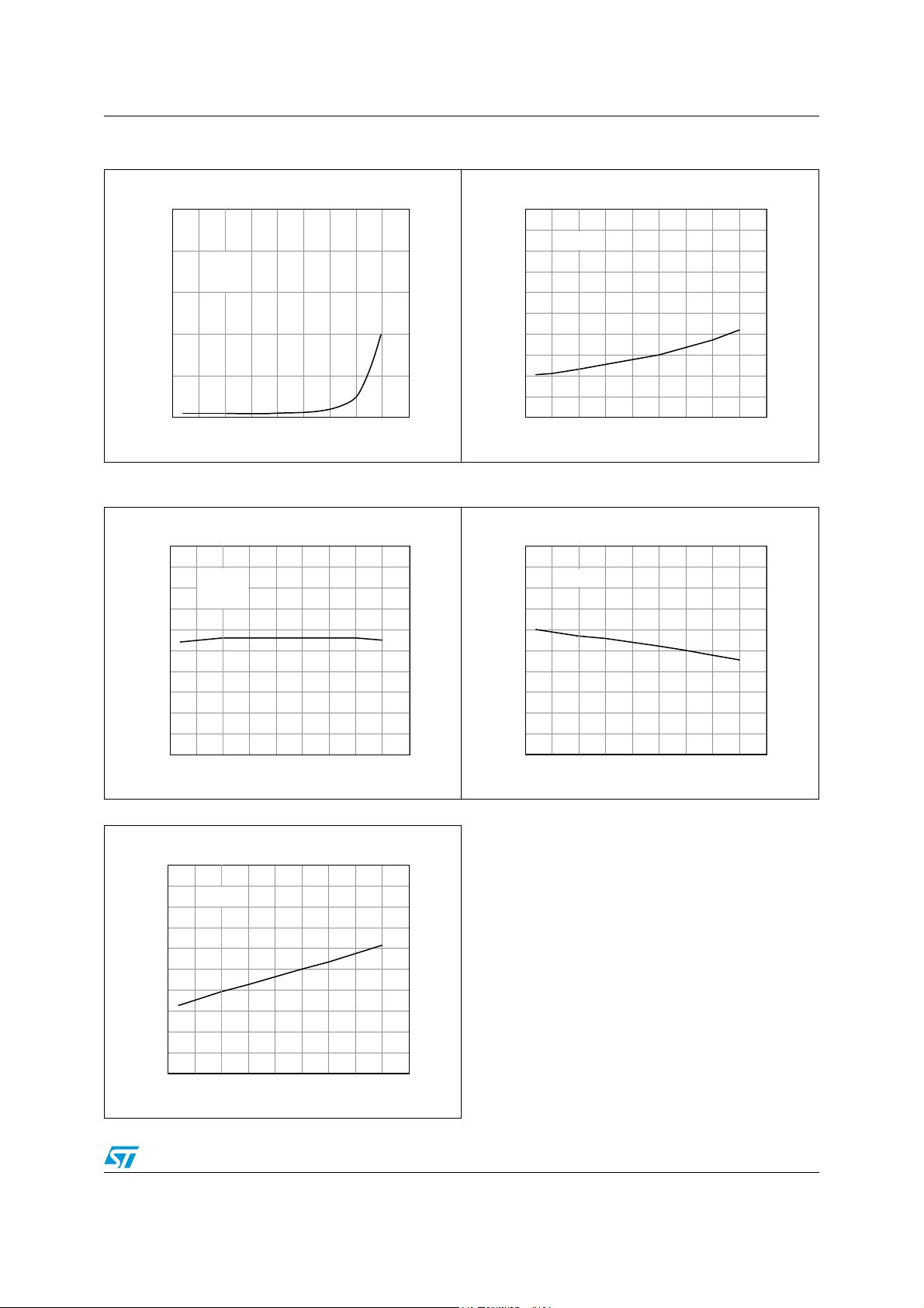
Figure 18. Status leakage current . . . . . . . . . . . . . . . . . . . . . . . . . . . . . . . . . . . . . . . . . . . . . . . . . . . . 17
Figure 19. Status low output voltage . . . . . . . . . . . . . . . . . . . . . . . . . . . . . . . . . . . . . . . . . . . . . . . . . . 17
Figure 20. Openload on-state detection threshold. . . . . . . . . . . . . . . . . . . . . . . . . . . . . . . . . . . . . . . . 17
Figure 21. Openload off-state voltage detection threshold . . . . . . . . . . . . . . . . . . . . . . . . . . . . . . . . . 17
Figure 22. Status clamp voltage . . . . . . . . . . . . . . . . . . . . . . . . . . . . . . . . . . . . . . . . . . . . . . . . . . . . . 17
Figure 23. Static drain source on resistance . . . . . . . . . . . . . . . . . . . . . . . . . . . . . . . . . . . . . . . . . . . . 18
Figure 24. Derating curve . . . . . . . . . . . . . . . . . . . . . . . . . . . . . . . . . . . . . . . . . . . . . . . . . . . . . . . . . . 18
Figure 25. Transconductance . . . . . . . . . . . . . . . . . . . . . . . . . . . . . . . . . . . . . . . . . . . . . . . . . . . . . . . 18
Figure 26. Transfer characteristics . . . . . . . . . . . . . . . . . . . . . . . . . . . . . . . . . . . . . . . . . . . . . . . . . . . 18
Figure 27. Turn-on current slope (V
Figure 28. Turn-on current slope (V
Figure 29. Input voltage vs input charge . . . . . . . . . . . . . . . . . . . . . . . . . . . . . . . . . . . . . . . . . . . . . . . 19
Figure 30. Capacitance variations . . . . . . . . . . . . . . . . . . . . . . . . . . . . . . . . . . . . . . . . . . . . . . . . . . . . 19
Figure 31. Switching time resistive load (V
Figure 32. Switching time resistive load (R
Figure 33. Output characteristics . . . . . . . . . . . . . . . . . . . . . . . . . . . . . . . . . . . . . . . . . . . . . . . . . . . . . 19
Figure 34. Step response current limit . . . . . . . . . . . . . . . . . . . . . . . . . . . . . . . . . . . . . . . . . . . . . . . . . 19
Figure 35. Source drain diode forward characteristics. . . . . . . . . . . . . . . . . . . . . . . . . . . . . . . . . . . . . 20
Figure 36. Static drian source on resistance vs I
Figure 37. Static drain source on resistance vs input voltage (I
Figure 38. Static drain source on resistance vs input voltage . . . . . . . . . . . . . . . . . . . . . . . . . . . . . . . 20
Figure 39. Normalized input threshold voltage vs temperature . . . . . . . . . . . . . . . . . . . . . . . . . . . . . . 20
Figure 40. Normalized on resistance vs temperature . . . . . . . . . . . . . . . . . . . . . . . . . . . . . . . . . . . . . 20
Figure 41. Turn-off drain source voltage slope (V
Figure 42. Turn-off drain source voltage slope (V
Figure 43. Current limit vs junction temperature . . . . . . . . . . . . . . . . . . . . . . . . . . . . . . . . . . . . . . . . . 21
Figure 44. Application diagram bridge drivers . . . . . . . . . . . . . . . . . . . . . . . . . . . . . . . . . . . . . . . . . . . 22
Figure 45. Recommended motor operation . . . . . . . . . . . . . . . . . . . . . . . . . . . . . . . . . . . . . . . . . . . . . 23
Figure 46. Waveforms . . . . . . . . . . . . . . . . . . . . . . . . . . . . . . . . . . . . . . . . . . . . . . . . . . . . . . . . . . . . . 24
Figure 47. SO-28 PC board . . . . . . . . . . . . . . . . . . . . . . . . . . . . . . . . . . . . . . . . . . . . . . . . . . . . . . . . . 25
Figure 48. Chipset configuration . . . . . . . . . . . . . . . . . . . . . . . . . . . . . . . . . . . . . . . . . . . . . . . . . . . . . 25
LIM
vs T
. . . . . . . . . . . . . . . . . . . . . . . . . . . . . . . . . . . . . . . . . . . . . . . . . . . . . . . . . . . . 16
case
. . . . . . . . . . . . . . . . . . . . . . . . . . . . . . . . . . . . . . . . . . . . . . . . 16
case
. . . . . . . . . . . . . . . . . . . . . . . . . . . . . . . . . . . . . . . . . . . . . . . . . 16
CC
=5V) . . . . . . . . . . . . . . . . . . . . . . . . . . . . . . . . . . . . . . . . . . . . . . 18
in
=3.5V) . . . . . . . . . . . . . . . . . . . . . . . . . . . . . . . . . . . . . . . . . . . . 18
in
=5V) . . . . . . . . . . . . . . . . . . . . . . . . . . . . . . . . . . . . . . . . 19
in
=10Ohm) . . . . . . . . . . . . . . . . . . . . . . . . . . . . . . . . . . . . . 19
g
. . . . . . . . . . . . . . . . . . . . . . . . . . . . . . . . . . . . . . . . 20
d
=3.5V). . . . . . . . . . . . . . . . . . . . . . . . . . . . . . . . . . 21
in
=5V) . . . . . . . . . . . . . . . . . . . . . . . . . . . . . . . . . . . 21
in
=7A) . . . . . . . . . . . . . . . . . . . . . . . . . 20
d
4/33 Doc ID 022022 Rev 1
Page 5

VN772KP-E List of figures
Figure 49. Auto and mutual Rthj-amb vs PCB copper area in open box free air condition . . . . . . . . . 25
Figure 50. SO-28 HSD thermal impedance junction ambient single pulse . . . . . . . . . . . . . . . . . . . . . 27
Figure 51. SO-28 LSD thermal impedance junction ambient single pulse. . . . . . . . . . . . . . . . . . . . . . 27
Figure 52. Thermal fitting model of an H-bridge in SO-28 . . . . . . . . . . . . . . . . . . . . . . . . . . . . . . . . . . 28
Figure 53. SO-28 package outline . . . . . . . . . . . . . . . . . . . . . . . . . . . . . . . . . . . . . . . . . . . . . . . . . . . . 29
Figure 54. Tube dimensions (no suffix) . . . . . . . . . . . . . . . . . . . . . . . . . . . . . . . . . . . . . . . . . . . . . . . . 31
Figure 55. Tape and reel dimensions (suffix “13TR”) . . . . . . . . . . . . . . . . . . . . . . . . . . . . . . . . . . . . . 31
Doc ID 022022 Rev 1 5/33
Page 6
Block diagram and pin description VN772KP-E
1 Block diagram and pin description
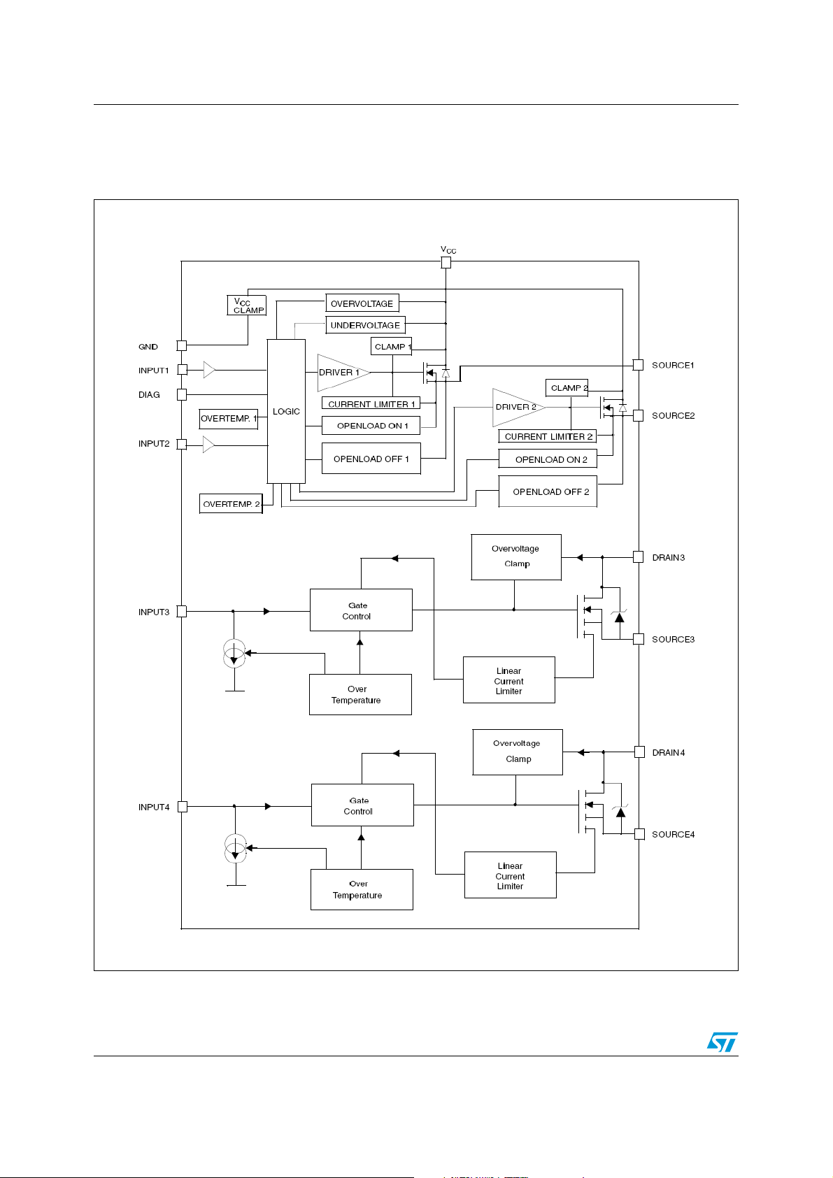
Figure 1. Block diagram
6/33 Doc ID 022022 Rev 1
Page 7
VN772KP-E Block diagram and pin description
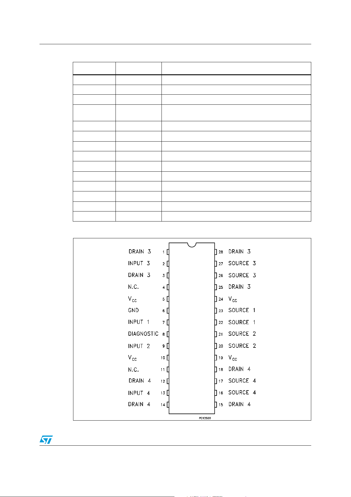
Table 2. Pin definition and function
No Name Function
1, 3, 25, 28 DRAIN 3 Drain of switch 3 (low-side switch)
2 INPUT 3 Input of switch 3 (low-side switch)
4, 11 N.C. Not connected
5, 10, 19, 24 V
CC
Drain of switches 1 and 2 (high-side switches) and power
supply voltage
6 GND Ground of switches 1 and 2 (high-side switches)
7 INPUT 1 Input of switch 1 (high-side switches)
8 DIAGNOSTIC Diagnostic of switches 1 and 2 (high-side switches)
9 INPUT 2 Input of switch 2 (high-side switch)
12, 14, 15, 18 DRAIN 4 Drain of switch 4 (low-side switch)
13 INPUT 4 Input of switch 4 (low-side switch)
16, 17 SOURCE 4 Source of switch 4 (low-side switch)
20, 21 SOURCE 2 Source of switch 2 (high-side switch)
22, 23 SOURCE 1 Source of switch 1 (high-side switch)
26, 27 SOURCE 3 Source of switch 3 (low-side switch)
Figure 2. Connection diagram
Doc ID 022022 Rev 1 7/33
Page 8
Electrical specifications VN772KP-E
2 Electrical specifications
2.1 Thermal data
Table 3. Thermal data
Symbol Parameter
R
thj-case
R
thj-case
R
thj-amb
Thermal resistance junction-case (high side switch) 20
Thermal resistance junction-case (low side switch) 20
Thermal resistance junction-ambient (with 6 cm2 of Cu heat sink) See Figure 49
2.2 Absolute maximum ratings
Table 4. Dual high side switch
Symbol Parameter Value Unit
DC supply voltage 41 V
V
CC
-V
-I
GND
I
OUT
-I
OUT
IIN DC input current ±10 mA
I
STAT
V
ESD
P
Tc Case operating temperature -40 to 150 °C
Reverse DC supply voltage -0.3 V
CC
DC reverse ground pin current -200 mA
DC output current Internally limited A
Reverse DC output current -6 A
DC status current ±10 mA
Electrostatic discharge (human body model:
R = 1.5 KΩ; C = 100 pF)
– Input
– Status
–Output
–V
CC
Power dissipation (T
tot
T
Junction operating temperature Internally limited °C
j
= 25°C) 6 W
C
4000
4000
5000
5000
Val u e Max
(°C/W)
V
V
V
V
T
Storage temperature -55 to 150 °C
stg
Table 5. Low side switch
Symbol Parameter Value Unit
Drain source voltage (V
V
DS
V
Input voltage Internally clamped V
IN
I
Input current ±20 mA
IN
= 0 V) Internally clamped V
IN
8/33 Doc ID 022022 Rev 1
Page 9

VN772KP-E Electrical specifications
Table 5. Low side switch (continued)
Symbol Parameter Value Unit
R
Minimum input series impedance 150 Ω
IN MIN
I
Drain current Internally limited A
D
V
ESD1
V
ESD2
I
Reverse DC output current -10.5 A
R
Electrostatic discharge (R = 1.5 KΩ, C = 100 pF) 4000 V
Electrostatic discharge on output pin only (human
body model: R = 330 Ω, C = 150 pF)
5000 V
P
Power dissipation (T
tot
T
Operating junction temperature Internally limited °C
j
= 25°C) 6 W
C
2.3 Electrical characteristics for dual high side switch
8V < V
Table 6. Power outputs (per each channel)
Symbol Parameter Test conditions Min Typ Max Unit
V
CC
V
USD
V
OV
R
I
S
I
L(off1)
I
L(off2)
I
L(off3
I
L(off4)
1. Per device.
< 36 V; -40°C < Tj < 150°C, unless otherwise specified.
CC
(1)
Operating supply voltage 5.5 13 36 V
(1)
Undervoltage shutdown 3 4 5.5 V
(1)
Overvoltage shutdown 36 V
I
= 2 A; Tj = 25°C 60 mΩ
On-state resistance
ON
OUT
I
= 2 A; VCC > 8 V 120 mΩ
OUT
Off-state; VCC = 13 V;
V
IN=VOUT
(1)
Supply current
Off-state; V
V
IN=VOUT
On-state; V
V
Off-state output current
IN=VOUT
T
= 125°C
j
Off-state output current VIN = 0 V; V
= V
V
) Off-state output current
Off-state output current
IN
T
= 125°C
j
V
IN=VOUT
=25°C
T
j
=0V
= 13 V;
CC
=0V; Tj = 25°C
= 13 V 5 7 mA
CC
=0V; VCC=36V;
= 3.5 V -75 0 µA
OUT
= 0 V; VCC=13V;
OUT
0 50 µA
=0V; VCC=13V;
12 40 µA
12 25 µA
5 µA
3 µA
Doc ID 022022 Rev 1 9/33
Page 10
Electrical specifications VN772KP-E
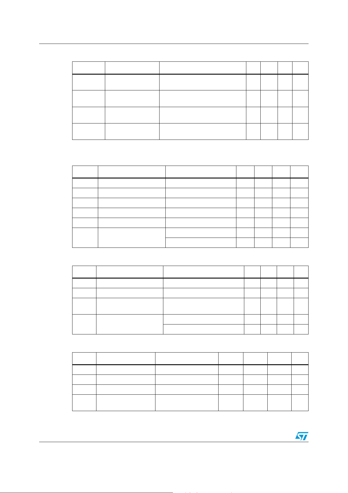
Table 7. Switching (per each channel) (VCC= 13V)
Symbol Parameter Test conditions Min Typ Max Unit
t
Tu r n - o n d el ay t i m e
d(on)
t
d(off)
dV
OUT
dV
OUT
1. See relative diagram
Table 8. Logic input (per each channel)
Turn-off delay time
/dt
Turn-on voltage slope
(on)
/dt
Turn-off voltage slope
(off)
RL=6.5Ω from VIN rising edge to
V
=1.3V
OUT
RL =6.5Ω from VIN falling edge to
V
= 11.7 V
OUT
RL=6.5Ω from V
V
= 10.4 V
OUT
=6.5Ω from V
R
L
=1.3V
V
OUT
= 1.3 V to
OUT
=11.7V to
OUT
—30 —µs
—30 —µs
(1)
(1)
—V/µs
—V/µs
—
—
Symbol Parameter Test conditions Min Typ Max Unit
Input low level 1.25 V
V
IL
I
Low level input current VIN = 1.25 V 1 µA
IL
V
Input high level 3.25 V
IH
I
High level input current VIN = 3.25 V 10 µA
IH
V
I(hyst)
V
Input hysteresis voltage 0.5 V
I
= 1 mA 6 6.8 8 V
Input clamp voltage
ICL
IN
I
= -1 mA -0.7 V
IN
Table 9. Status pin (per each channel)
Symbol Parameter Test conditions Min Typ Max Unit
V
I
LSTAT
C
V
Table 10. Protections (per each channel)
Status low output voltage I
STAT
STAT
Status leakage current Normal operation; V
Status pin input
STAT
capacitance
Status clamp voltage
SCL
Normal operation; V
I
STAT
I
STAT
= 1.6 mA 0.5 V
=5V 10 µA
STAT
= 5 V 100 pF
STAT
= 1 mA 6 6.8 8 V
= -1 mA -0.7 V
Symbol Parameter Test conditions Min Typ Max Unit
T
T
t
Shutdown temperature 150 175 200 °C
TSD
T
Reset temperature 135 °C
R
Thermal hysteresis 7 15 °C
hyst
Status delay in overload
SDL
conditions
T
j>TTSD
20 µs
10/33 Doc ID 022022 Rev 1
Page 11
VN772KP-E Electrical specifications
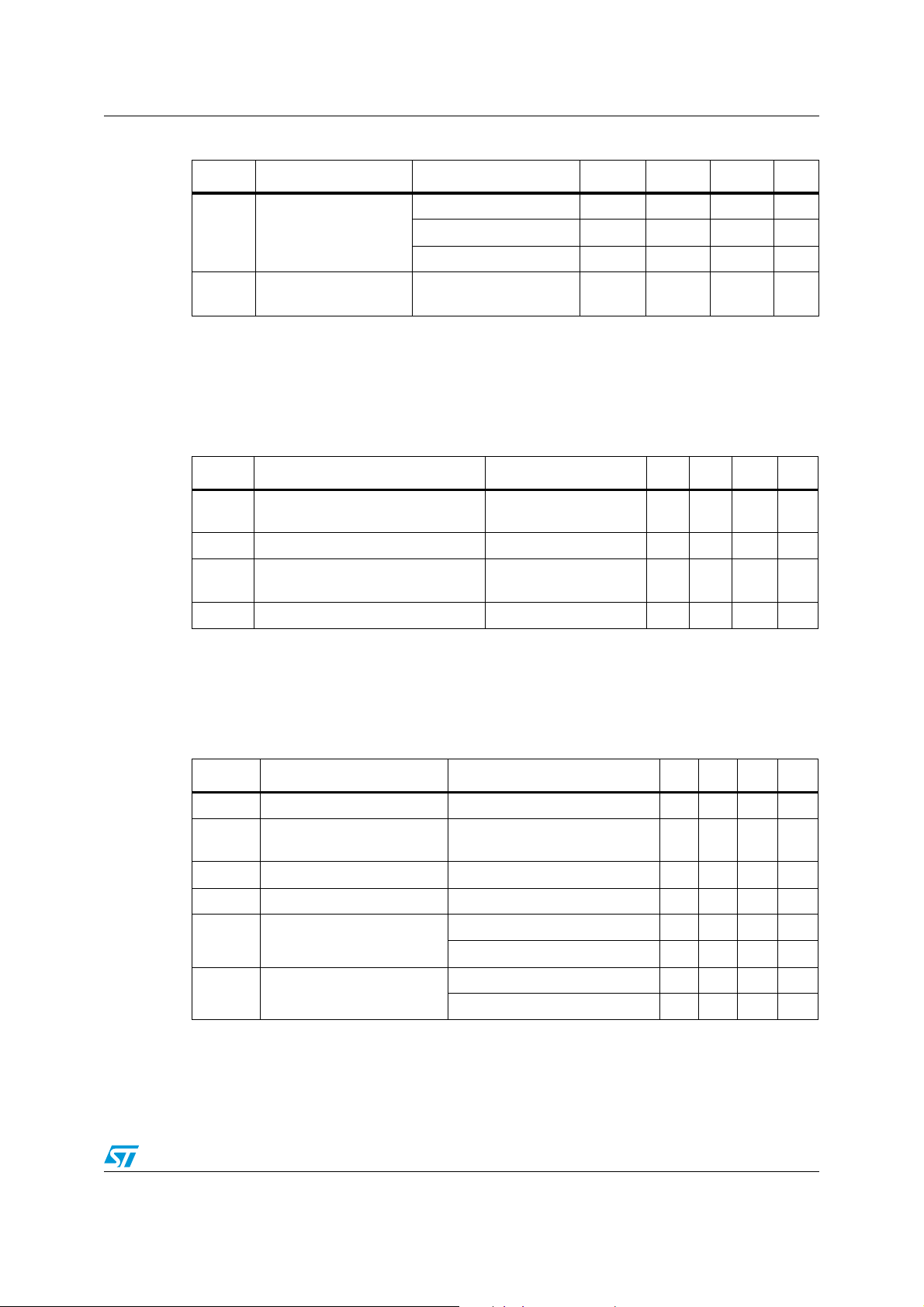
Table 10. Protections (per each channel) (continued)
Symbol Parameter Test conditions Min Typ Max Unit
6915A
I
Current limitation
lim
Tj = 125°C 8.5 15 A
5.5 V < VCC<36V 15 A
Turn-off output clamp
V
demag
voltage
=2A; L=6mH VCC-41 VCC-48 VCC-55 V
I
OUT
Note: To ensure long term reliability under heavy overload or short circuit conditions, protection
and related diagnostic signals must be used together with a proper software strategy. If the
device is subjected to abnormal conditions, this software must limit the duration and number
of activation cycles.
Table 11. Openload detection (per each channel)
Symbol Parameter Test conditions Min Typ Max Unit
Openload on-state detection
I
OL
threshold
VIN = 5 V 50 100 200 mA
t
DOL(on)
V
t
DOL(off)
Openload on-state detection delay I
Openload off-state voltage
OL
detection threshold
= 0 A 200 µs
OUT
V
= 0 V 1.5 2.5 3.5 V
IN
Openload detection delay at turn-off 1000 µs
2.4 Electrical characteristics for low side switches
-40°C < Tj < 150°C, unless otherwise specified.
Table 12. Off-state
Symbol Parameter Test conditions Min Typ Max Unit
V
Drain source clamp voltage VIN =0V; ID = 3.5 A 40 45 55 V
CLAMP
V
V
I
V
I
CLTH
INTH
DSS
Drain source clamp
threshold voltage
=0V; ID =2mA 36 V
V
IN
Input threshold voltage VDS =VIN; ID = 1 mA 0.5 2.5 V
Supply current from input pin VDS =0V; VIN = 5 V 100 150 µA
ISS
I
= 1 mA 6 6.8 8 V
Input-source clamp voltage
INCL
Zero input voltage drain
current (V
=0V)
IN
IN
I
= -1 mA -1.0 -0.3 V
IN
VDS=13V; VIN=0V; Tj=25°C 30 µA
V
=25V; VIN=0V 75 µA
DS
Doc ID 022022 Rev 1 11/33
Page 12
Electrical specifications VN772KP-E
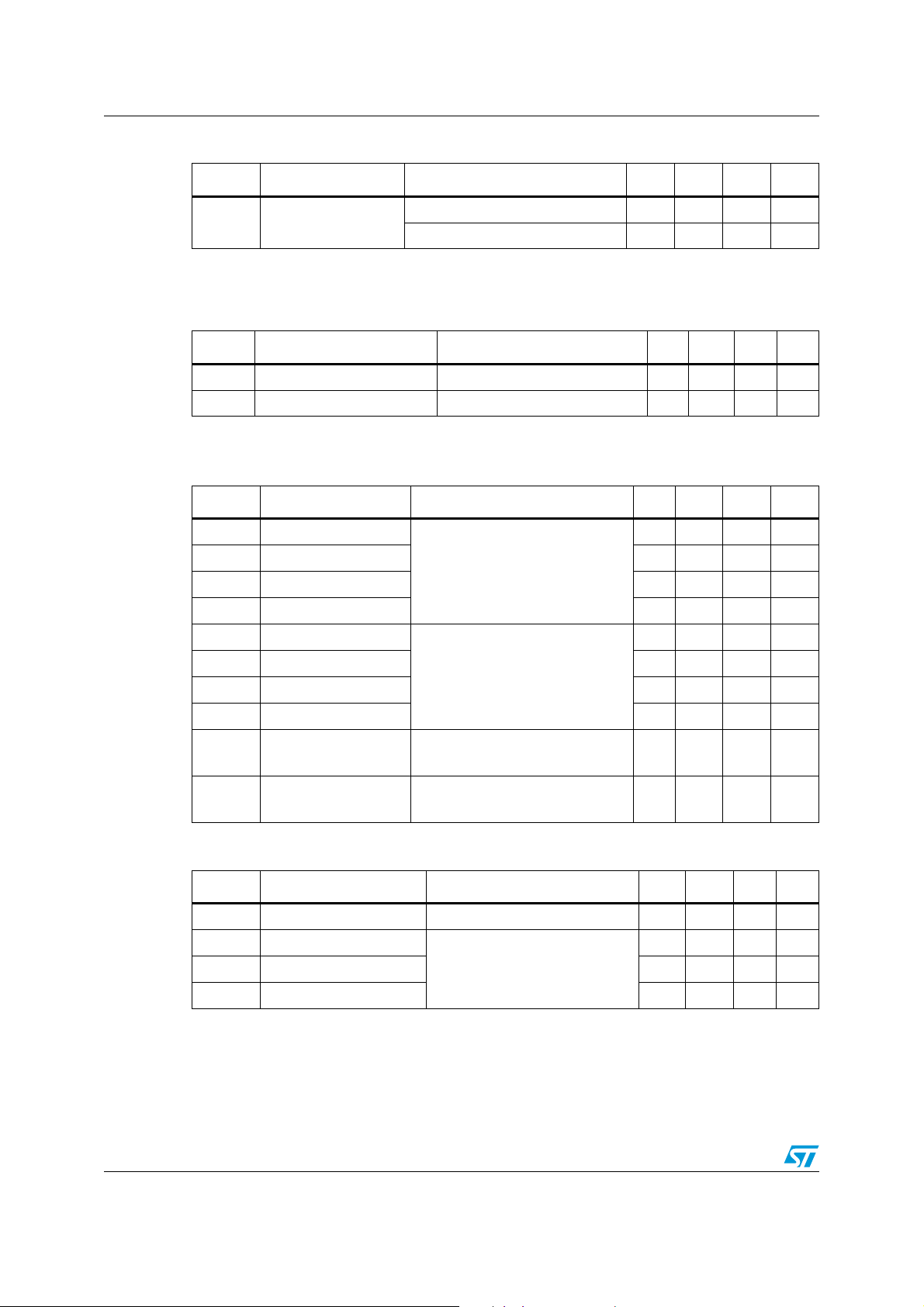
Table 13. On-state
Symbol Parameter Test conditions Min Typ Max Unit
V
=5V; ID = 3.5 A; Tj = 25°C — — 65 mΩ
R
DS(on)
T
= 25°C, unless otherwise specified.
j
Table 14. Dynamic
Static drain source on
resistance
Symbol Parameter Test conditions Min Typ Max Unit
(1)
g
Forward trans conductance VDD =13 V; ID = 3.5 A — 9 — S
fs
C
Output capacitance V
OSS
1. Pulsed: Pulse duration = 300 µs, duty cycle 1.5%
Table 15. Switching
Symbol Parameter Test conditions Min Typ Max Unit
Turn-on delay time
t
d(on)
t
Rise time — 470 1500 ns
r
t
Turn-off delay time — 500 1500 ns
d(off)
t
Fall time — 350 1000 ns
f
t
Turn-on delay time
d(on)
t
Rise time — 4.6 14 µs
r
t
d(off)
(dI/dt)
Turn-off delay time — 5.4 16 µs
t
Fall time — 3.6 11 µs
f
Turn-on current slope
on
Q
Total input charge
i
IN
VIN =5V; ID = 3.5 A — — 130 mΩ
= 13 V; f = 1 MHz; VIN = 0 V — 220 — pF
DS
— 100 300 ns
=15V; ID =3.5A; V
V
DD
R
gen=RIN MIN
= 150 Ω
gen
=5V;
—0.75 2.3 µs
= 15 V; ID =3.5A; V
V
DD
R
=2.2KΩ
gen
=15V; ID =3.5A; V
V
DD
= R
R
gen
=12 V; ID = 3.5 A; VIN =5V;
V
DD
= 2.13 mA
I
gen
IN MIN
= 150 Ω
gen
gen
=5V;
=5V;
—6.5 A/µs
—18 nC
Table 16. Source drain diode
Symbol Parameter Test conditions Min Typ Max Unit
(1)
V
SD
Q
I
RRM
1. Pulsed: Pulse duration = 300 µs, duty cycle 1.5%
Forward on voltage ISD = 3.5 A; VIN =0V — 0.8 — V
t
Reverse recovery time
rr
Reverse recovery charge — 0.28 — µC
rr
ISD= 3.5 A; dI/dt = 20 A/µs;
V
=30V; L=200µH
DD
Reverse recovery current — 2.5 — A
12/33 Doc ID 022022 Rev 1
—220—ns
Page 13
VN772KP-E Electrical specifications
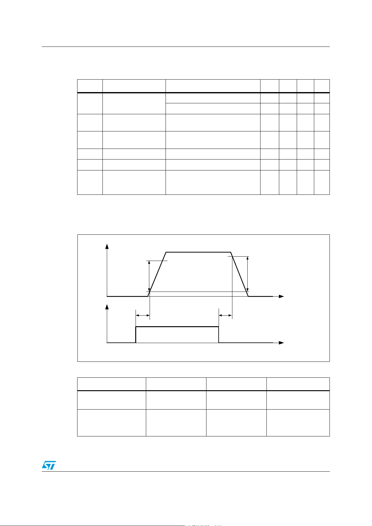
-40°C < Tj < 150°C, unless otherwise specified.
Table 17. Protections
Symbol Parameter Test conditions Min Typ Max Unit
V
=5V; VDS=13V 6 9 12 A
I
Drain current limit
lim
t
T
E
Step response current
dlim
limit
Over temperature
jsh
shutdown
Over temperature reset 135 °C
T
jrs
I
Fault sink current VIN = 5 V; VDS =13V; Tj =T
gf
Single pulse avalanche
as
energy
IN
V
=5V; VDS=13V; Tj= 125°C 6.5 12 A
IN
=5V; VDS = 13 V 4 µs
V
IN
150 175 °C
15 mA
jsh
Starting T
V
IN
=25°C; VDD=24V;
j
=5V; R
gen=RIN MIN
=150Ω;
200 mJ
L=24mH
2.5 Dual high-side switch timing data
Figure 3. Switching time waveforms
9
287Q
GW
G9
RQ
287
9
,1Q
Table 18. Truth table
Conditions Input Output Status
Normal operation
GW
RQ
L
H
GW
G9
RII
287
W
GW
RII
W
*$3*&)7
L
H
H
H
Current limitation
L
H
H
X
X
L
H
(Tj < TTSD) H
(T
j > TTSD) L
Doc ID 022022 Rev 1 13/33
Page 14
Electrical specifications VN772KP-E
Table 18. Truth table (continued)
Conditions Input Output Status
Over temperature
Undervoltage
Overvoltage
Output voltage > V
Output current < I
OL
OL
L
H
L
H
L
H
L
H
L
H
L
L
L
L
L
L
H
H
L
H
Figure 4. Open-load status timing (with external pull-up)
!9
9
9
,1Q
67$7 Q
9
287
2/
,
287
,
H
L
X
X
H
H
L
H
H
L
2/
W
'2/RII
Figure 5. Over temperature status timing
!7
7
M
9
,1Q
9
67$7 Q
W
6'/
14/33 Doc ID 022022 Rev 1
76'
W
'2/RQ
W
6'/
*$3*&)7
*$3*&)7
Page 15
VN772KP-E Electrical specifications
2.6 Electrical characterization for dual high side switch
Figure 6. Off-state output current Figure 7. Input clamp voltage
IL(off1) (uA)
2.5
2.25
2
1.75
1.5
1.25
1
0.75
0.5
0.25
0
-50 -25 0 25 50 75 100 125 150 175
Off state
Vcc=36V
Vin=Vout=0V
Tc (°C)
Figure 8. High level input current Figure 9. Input high level voltage
Iih (uA)
5
4.5
3.5
2.5
1.5
0.5
Vin=3.25V
4
3
2
1
0
-50 -25 0 25 50 75 100 125 150 175
Tc (°C)
Figure 10. Input low level voltage Figure 11. Input hysteresis voltage
Vil (V)
2.6
2.4
2.2
2
1.8
1.6
1.4
1.2
1
-50 -25 0 25 50 75 100 125 150 175
Tc ( ºC )
Vicl (V)
8
7.8
7.6
7.4
7.2
7
6.8
6.6
6.4
6.2
6
Iin=1mA
-50 -25 0 25 50 75 100 125 150 175
Tc (°C)
Vih (V)
3.6
3.4
3.2
3
2.8
2.6
2.4
2.2
2
-50 -25 0 25 50 75 100 125 150 175
Tc (°C)
Vhyst (V)
1.5
1.4
1.3
1.2
1.1
1
0.9
0.8
0.7
0.6
0.5
-50 -25 0 25 50 75 100 125 150 175
Tc (°C)
Doc ID 022022 Rev 1 15/33
Page 16
Electrical specifications VN772KP-E
Figure 12. Overvoltage shutdown Figure 13. I
Vov (V)
50
48
46
44
42
40
38
36
34
32
30
-50 -25 0 25 50 75 100 125 150 175
Tc (°C)
Ilim (A)
20
18
16
14
12
10
8
6
4
2
0
-50 -25 0 25 50 75 100 125 150 175
vs T
LIM
Vcc=13V
case
Tc (°C)
Figure 14. Turn-on voltage slope Figure 15. Turn-off voltage slope
dVout/dt(on) (V/ms)
800
700
600
500
400
300
200
100
Vcc=13V
Rl=6.5Ohm
0
-50 -25 0 25 50 75 100 125 150 175
Tc (ºC)
dVout/dt(off) (V/ms)
600
550
500
450
400
350
300
250
200
Vcc=13V
Rl=6.5O hm
-50 -25 0 25 50 75 100 125 150 175
Tc (ºC)
Figure 16. On-state resistance vs T
case
Ron (mOhm)
160
140
120
100
80
60
40
20
0
-50 -25 0 25 50 75 100 125 150 175
Iout=2A
Vcc=8V; 13V & 36V
Figure 17. On-state resistance vs V
Ron (mOhm)
120
110
100
90
80
70
60
50
40
30
20
10
Tc (°C)
16/33 Doc ID 022022 Rev 1
CC
Tc=150°C
Tc=25°C
Tc= - 40°C
Iout=5A
0
5 10152025303540
Vcc (V)
Page 17
VN772KP-E Electrical specifications
Figure 18. Status leakage current Figure 19. Status low output voltage
Ilstat (uA)
0.05
0.04
Vstat=5V
0.03
0.02
0.01
0
-50 -25 0 25 50 75 100 125 150 175
Tc (°C)
Vstat (V)
1
0.9
0.8
0.7
0.6
0.5
0.4
0.3
0.2
Istat=1.6mA
0.1
0
-50 -25 0 25 50 75 100 125 150 175
Tc ( ºC )
Figure 20. Openload on-state detection
threshold
Iol (mA)
150
140
130
120
110
100
90
80
70
60
50
Vcc=13V
Vin=5V
-50 -25 0 25 50 75 100 125 150 175
Tc (ºC)
Figure 22. Status clamp voltage
Vscl (V)
8
7.8
7.6
7.4
7.2
6.8
6.6
6.4
6.2
Istat=1mA
7
6
-50 -25 0 25 50 75 100 125 150 175
Tc (°C)
Figure 21. Openload off-state voltage
detection threshold
Vol (V)
5
4.5
4
3.5
3
2.5
2
1.5
1
0.5
0
Vin=0V
-50 -25 0 25 50 75 100 125 150 175
Tc ( ºC )
Doc ID 022022 Rev 1 17/33
Page 18
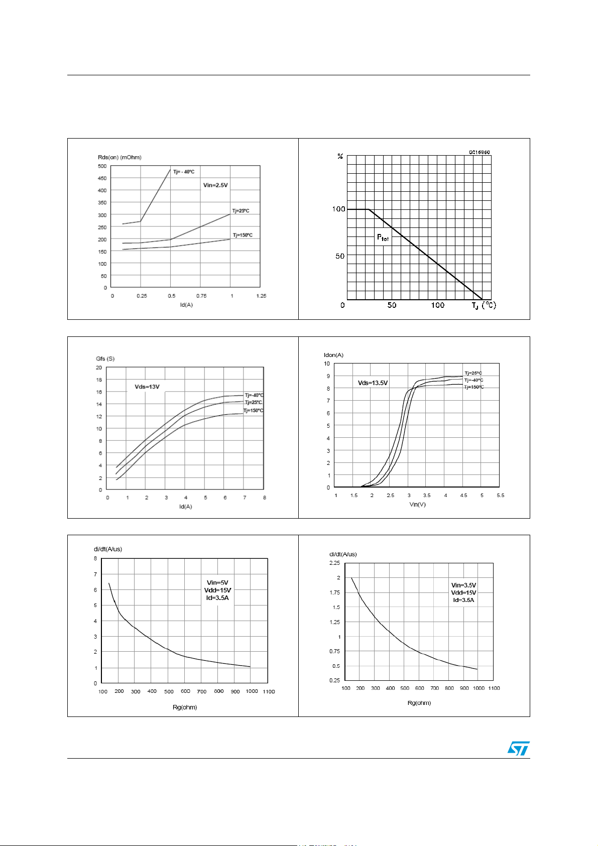
Electrical specifications VN772KP-E
2.7 Electrical characterization for low side switches
Figure 23. Static drain source on resistance Figure 24. Derating curve
Figure 25. Transconductance Figure 26. Transfer characteristics
Figure 27. Turn-on current slope (Vin=5V) Figure 28. Turn-on current slope (Vin=3.5V)
18/33 Doc ID 022022 Rev 1
Page 19
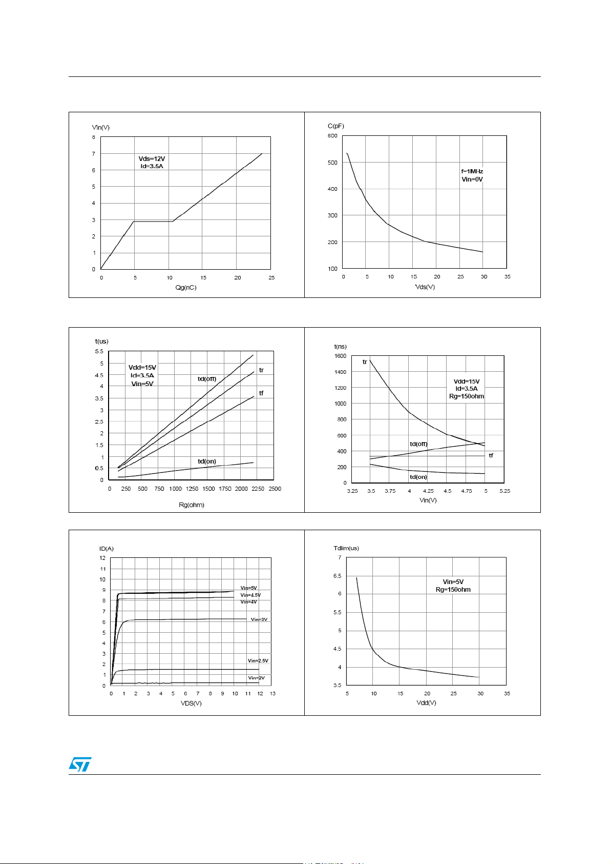
VN772KP-E Electrical specifications
Figure 29. Input voltage vs input charge Figure 30. Capacitance variations
Figure 31. Switching time resistive load
(V
=5V)
in
Figure 32. Switching time resistive load
(Rg=10Ohm)
Figure 33. Output characteristics Figure 34. Step response current limit
Doc ID 022022 Rev 1 19/33
Page 20
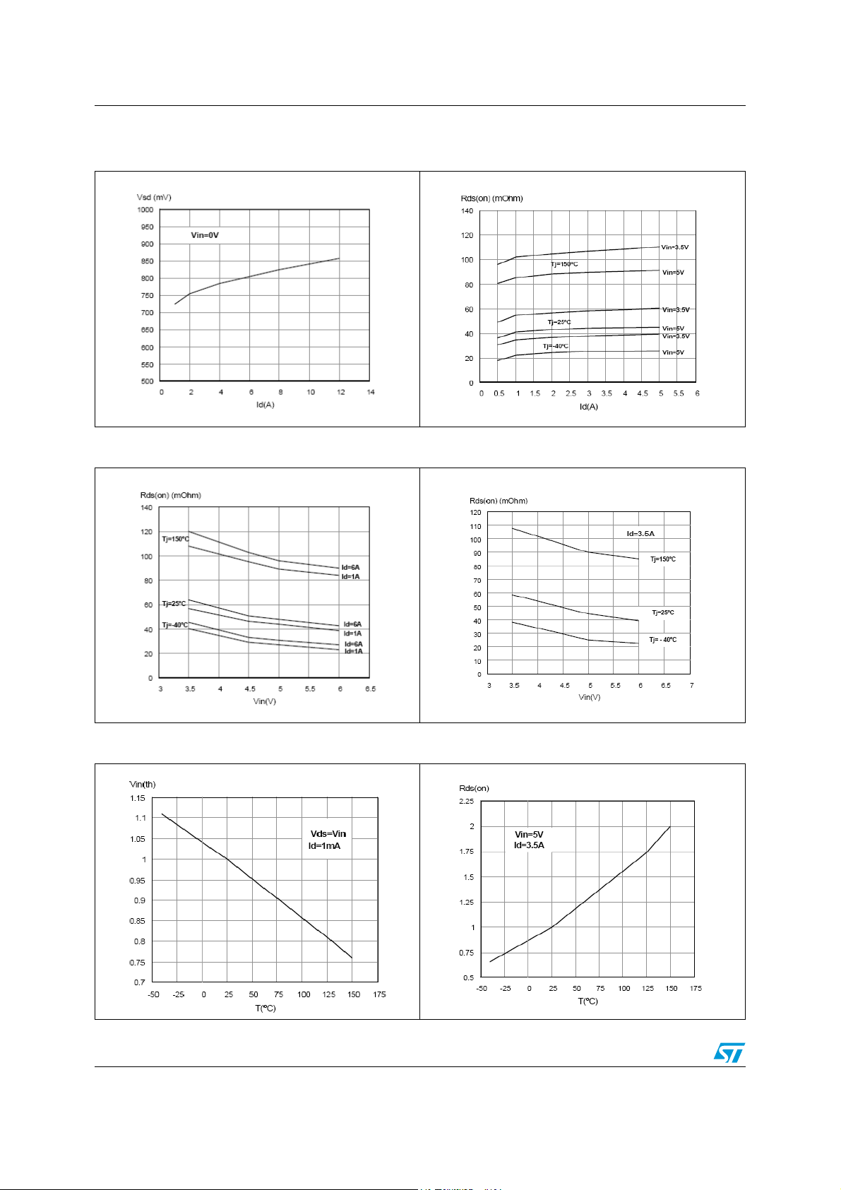
Electrical specifications VN772KP-E
Figure 35. Source drain diode forward
characteristics
v
Figure 37. Static drain source on resistance vs
input voltage (I
=7A)
d
Figure 36. Static drian source on resistance vs
I
d
Figure 38. Static drain source on resistance vs
input voltage
Figure 39. Normalized input threshold voltage
Figure 40. Normalized on resistance vs
vs temperature
20/33 Doc ID 022022 Rev 1
temperature
Page 21
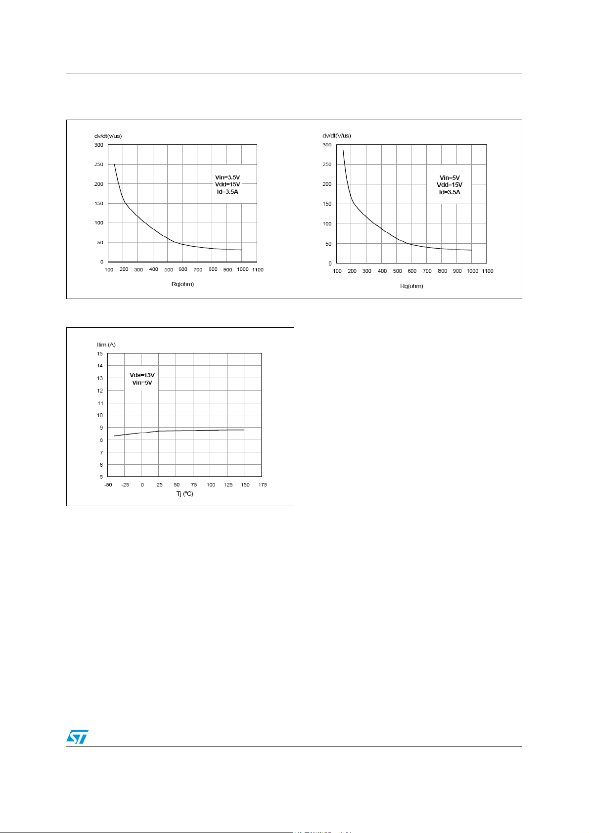
VN772KP-E Electrical specifications
Figure 41. Turn-off drain source voltage slope
(V
=3.5V)
in
Figure 43. Current limit vs junction
temperature
Figure 42. Turn-off drain source voltage slope
(Vin=5V)
Doc ID 022022 Rev 1 21/33
Page 22
Application recommendations VN772KP-E
3 Application recommendations
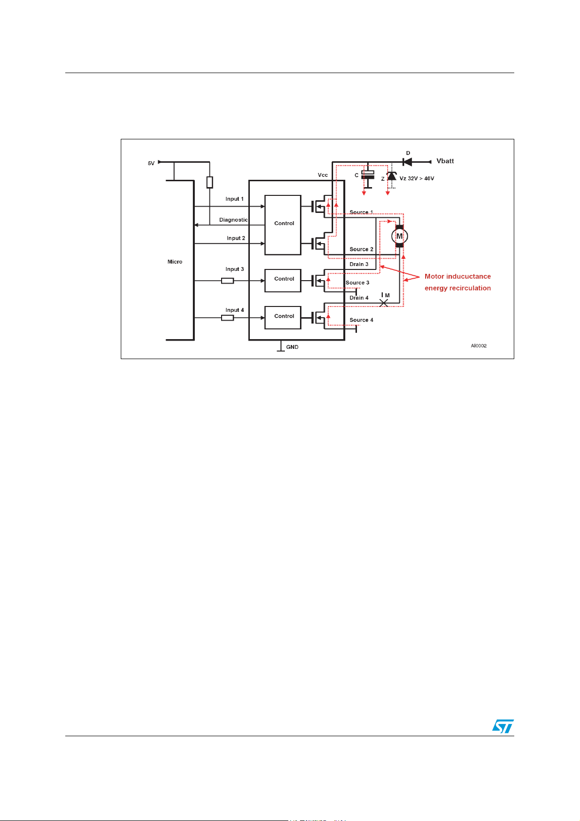
Figure 44. Application diagram bridge drivers
Most motor bridge drivers use a reverse battery protection diode (D) inside the supply rail.
This diode prevents a reverse current flow back to V
in case the bridge becomes
BATT
disabled via the logic inputs while motor inductance still carries energy. In order to prevent a
hazardous overvoltage at circuit supply terminal (V
), a blocking capacitor (C) is needed to
CC
limit the voltage overshoot. As basic orientation, 50µF per 1A load current is recommended.
As an alternative, a Zener protection (Z) is also suitable.
Even if a reverse polarity diode is not present, it is recommended to use a capacitor or
Zener at V
because a similar problem appears in case the supply terminal of the module
CC
has intermittent electrical contact to the battery or gets disconnected while the motor is
operating.
22/33 Doc ID 022022 Rev 1
Page 23
VN772KP-E Application recommendations
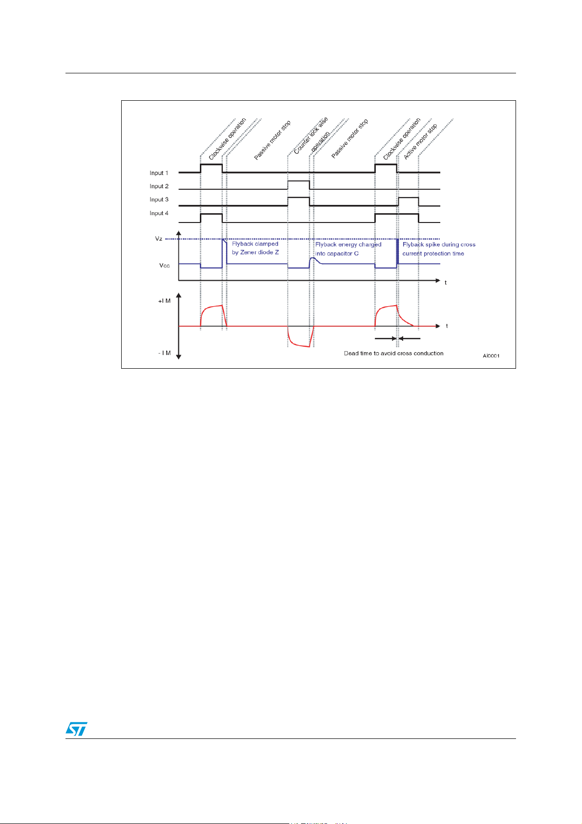
Figure 45. Recommended motor operation
Doc ID 022022 Rev 1 23/33
Page 24
Application recommendations VN772KP-E
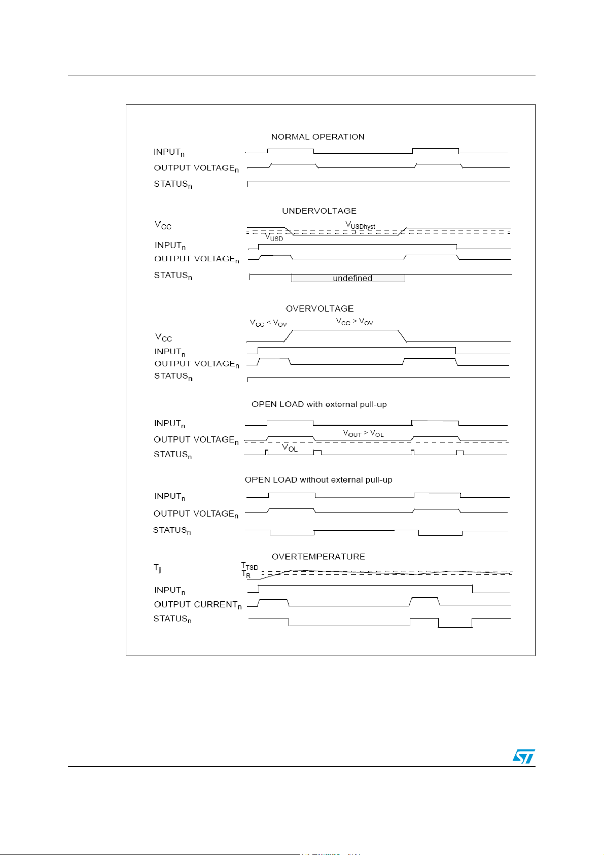
Figure 46. Waveforms
24/33 Doc ID 022022 Rev 1
Page 25
VN772KP-E Thermal data
4 Thermal data
4.1 SO-28 thermal data
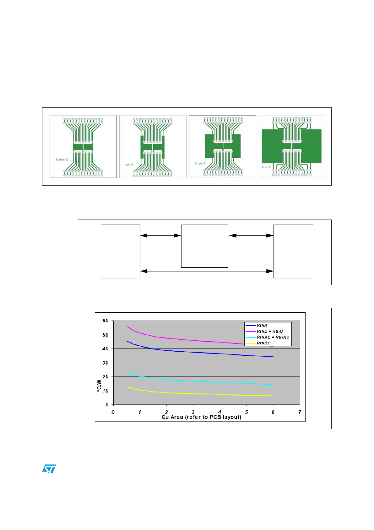
Figure 47. SO-28 PC board
Note: Layout condition of Rth and Zth measurements (PCB FR4 area = 58mm x 58mm, PCB
thickness = 2mm, Cu thickness = 35µm, Copper areas: from minimum pad layout to 6cm
Figure 48. Chipset configuration
LOW SIDE
CHIP
R
thAB
HIGH SIDE
CHIP
R
thAC
LOW SIDE
CHIP
channel 1,2
channel 3
R
thB
R
R
thA
thBC
channel 4
R
thC
Figure 49. Auto and mutual Rthj-amb vs PCB copper area in open box free air
condition
(a)
2
).
a. see definitions in Section 5.3 on page 31
Doc ID 022022 Rev 1 25/33
Page 26

Thermal data VN772KP-E
4.2 Thermal calculation in clockwise and anti-clockwise operation in steady state mode
Table 19. Thermal calculation in clockwise and anti-clockwise operation in steady state mode
HS1 HS2 LS
On Off Off On
Off On On Off
LS
3
4
P
P
dHS1
dHS2
x R
R
thHSLS
x R
R
thHSLS
T
jHS12
thHS
thHS
+ P
+ T
+ P
+ T
dLS4
amb
dLS3
amb
T
jLS3
x
x
P
P
dHS1
x R
dHS2
x R
x R
x R
thHSLS
thLSLS
thHSLS
thLS
+ T
+ T
+ P
amb
+ P
amb
dLS4
dLS3
P
dHS1
P
dHS2
x R
R
x R
R
thLSLS
T
thHSLS
thLS
thHSLS
jLS4
+ T
+ T
+ P
amb
+ P
amb
dLS4
dLS3
4.2.1 Thermal resistances definition
Values according to the PCB heatsink area.
R
= R
thHS
in on-state)
R
= R
thLS
R
thHSLS
= R
high side and low side chips
R
thLSLS
= R
4.2.2 Thermal calculation in transient mode
T
= Z
jHS12
T
= Z
jLS3
T
= Z
jLS4
thHS1
thLS3
thHS1LS4
thLS3LS4
thHS
thHSLS
thHSLS
= R
= R
= high side chip thermal resistance junction to ambient (HS1 or HS2
thHS2
= low side chip thermal resistance junction to ambient
thLS4
= R
thHS2LS3
= mutual thermal resistance junction to ambient between
= mutual thermal resistance junction to ambient between low side chips
(b)
x P
x P
x P
dHS12
dHS12
dHS12
+ Z
+ Z
+ Z
thHSLS
thLS
thLSLS
x (P
x P
x P
dLS3
dLS3
dLS3
+ Z
+ P
thLSLS
+ Z
dLS4
thLS
) + T
x P
x P
amb
dLS4
dLS4
+ T
+ T
amb
amb
x
x
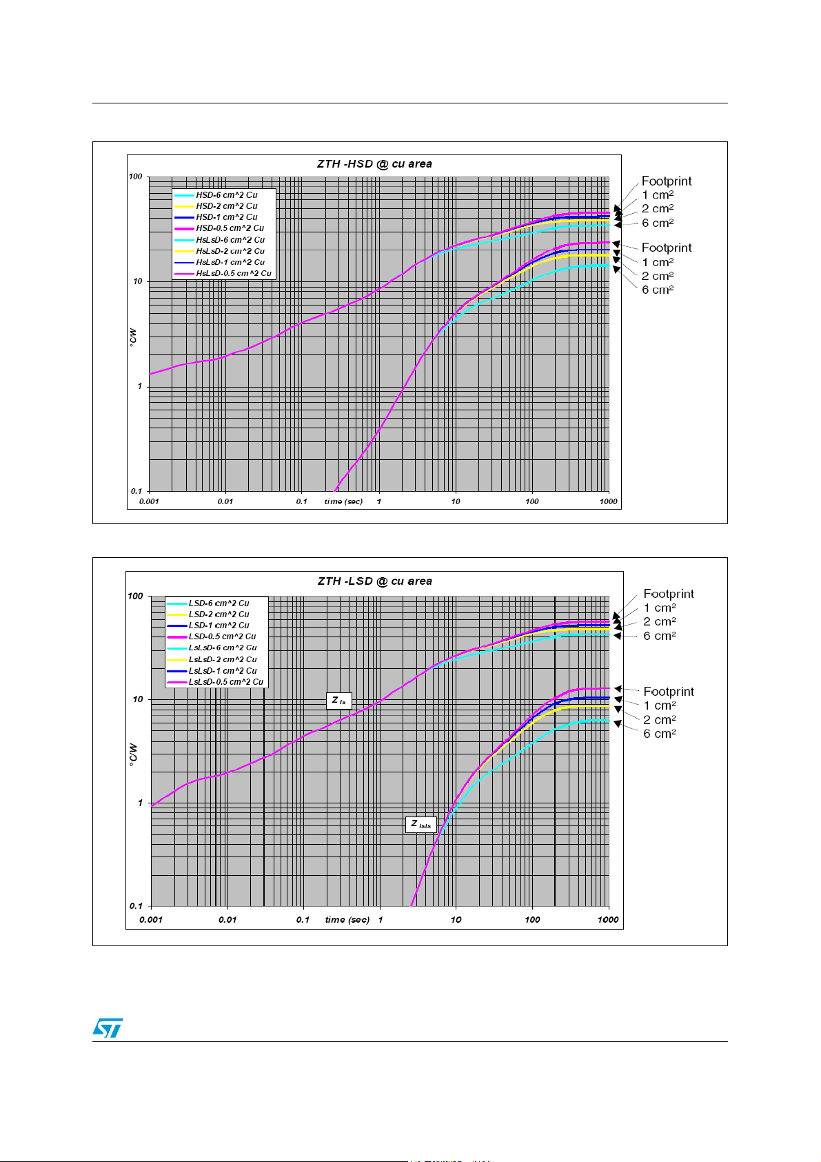
4.2.3 Single pulse thermal impedance definition
Values according to the PCB heatsink area.
Z
= high side chip thermal impedance junction to ambient
thHS
Z
thLS
Z
thHSLS
= Z
thLS3
= Z
= Z
thLS4
thHS12LS3
= low side chip thermal impedance junction to ambient
= Z
thHS12LS4
= mutual thermal impedance junction to ambient between
high side and low side chips
Z
thLSLS
= Z
thLS3LS4
= mutual thermal impedance junction to ambient between low side chips
4.2.4 Pulse calculation formula
Z
THδ
where δ = tP/T
b. Calculation is valid in any dynamic operating condition. Pd values set by user.
26/33 Doc ID 022022 Rev 1
RTHδ Z
THtp
1 δ–()+⋅=
Page 27
VN772KP-E Thermal data
Figure 50. SO-28 HSD thermal impedance junction ambient single pulse
Figure 51. SO-28 LSD thermal impedance junction ambient single pulse
Doc ID 022022 Rev 1 27/33
Page 28
Thermal data VN772KP-E
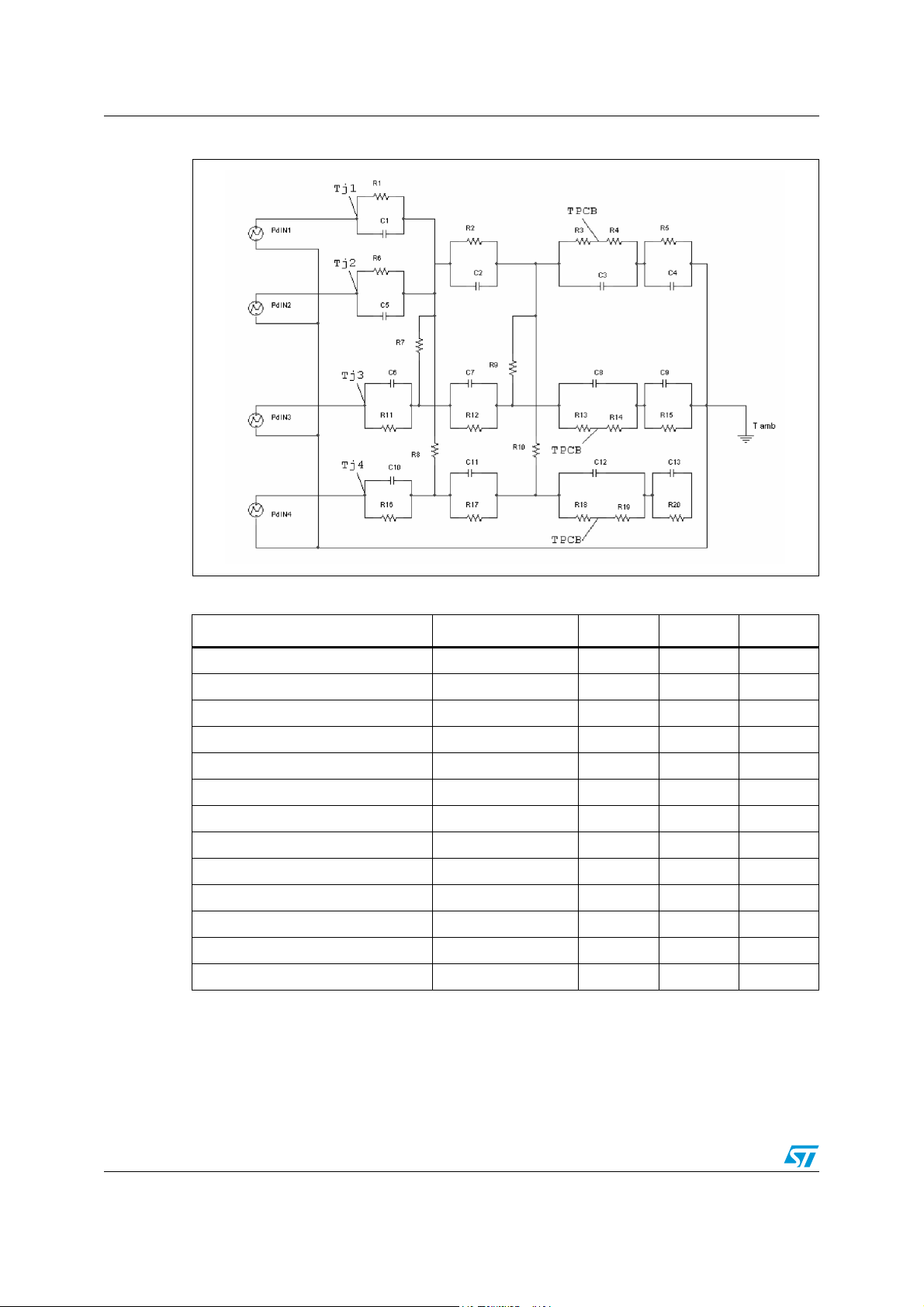
Figure 52. Thermal fitting model of an H-bridge in SO-28
Table 20. Thermal parameters
(1)
Area/island (cm2) Footprint 1 2 6
R1 = R6 (°C/W) 1.5
R2 (°C/W) 2.6
R12 = R17 (°C/W) 3.5
R3 = R13 = R 18 (°C/W) 15.5
R4 = R14 = R19 (°C/W) 10.5
R5 = R15 = R20 (°C/W) 62.28 52.28 44.28 32.28
R7 = R8 = R9 = R10 (°C/W) 150
R11 = R16 (°C/W) 1.5
C1 = C5 (W.s/°C) 0.00035
C2 = C7 = C11 (W.s/°C) 0.024
C3 = C8 =C 12 (W.s/°C) 0.2
C4 = C9 = C13 (W.s/°C) 1.6 1.61 1.7 3.25
C6 = C10 (W.s/°C) 0.00075
1. The blank space means that the value is the same as the previous one.
28/33 Doc ID 022022 Rev 1
Page 29
VN772KP-E Package mechanical data
5 Package mechanical data
5.1 ECOPACK® package
In order to meet environmental requirements, ST offers these devices in different grades of
ECOPACK
specifications, grade definitions and product status are available at: www.st.com
ECOPACK
®
packages, depending on their level of environmental compliance. ECOPACK®
®
is an ST trademark.
5.2 SO-28 mechanical data
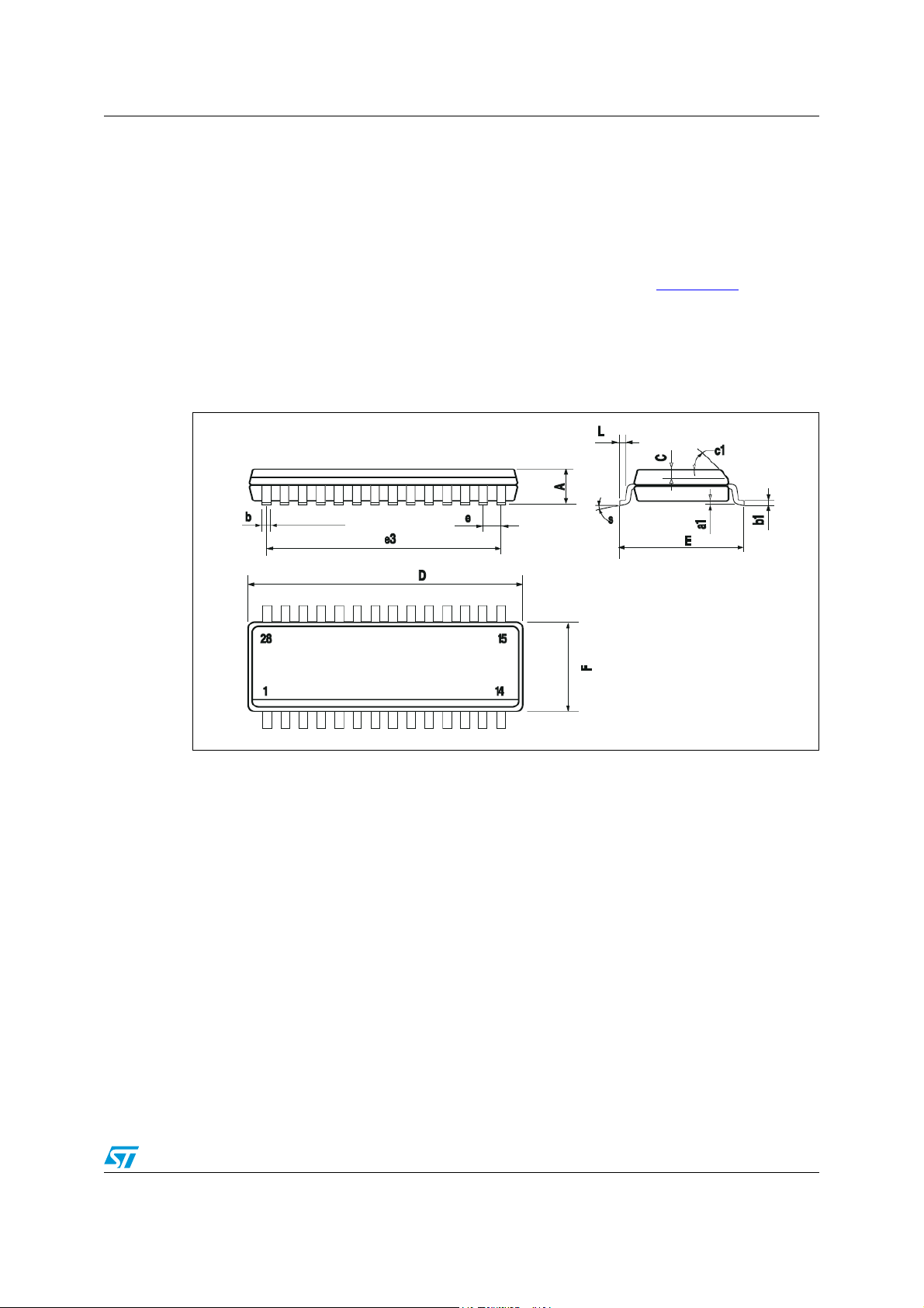
Figure 53. SO-28 package outline
.
Doc ID 022022 Rev 1 29/33
Page 30
Package mechanical data VN772KP-E
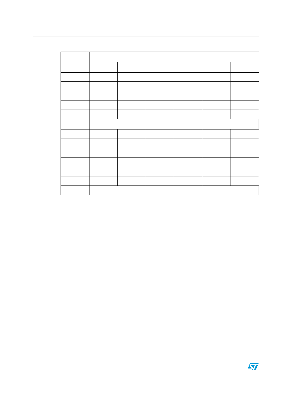
Table 21. SO-28 mechanical data
mm inch
DIM
Min. Typ Max. Min. Typ. Max.
A 2.65 0.104
a1 0.1 0.3 0.004 0.012
b 0.35 0.49 0.013 0.019
b1 0.23 0.32 0.009 0.012
C 0.5 0.020
c1 45° (typ.)
D 17.7 18.1 0.697 0.713
E 10 10.65 0.393 0.419
e 1.27 0.050
e3 16.51 0.650
F 7.4 7.6 0.291 0.299
L 0.4 1.27 0.016 0.050
S 8° (max.)
30/33 Doc ID 022022 Rev 1
Page 31
VN772KP-E Package mechanical data
5.3 SO-28 tube shipment
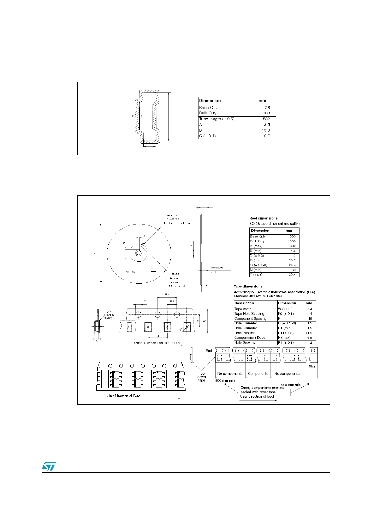
Figure 54. Tube dimensions (no suffix)
5.4 Tape and reel shipment
Figure 55. Tape and reel dimensions (suffix “13TR”)
Doc ID 022022 Rev 1 31/33
Page 32
Revision history VN772KP-E
6 Revision history
Table 22. Document revision history
Date Revision Changes
21-Jul-2011 1 Initial release.
32/33 Doc ID 022022 Rev 1
Page 33

VN772KP-E
Please Read Carefully:
Information in this document is provided solely in connection with ST products. STMicroelectronics NV and its subsidiaries (“ST”) reserve the
right to make changes, corrections, modifications or improvements, to this document, and the products and services described herein at any
time, without notice.
All ST products are sold pursuant to ST’s terms and conditions of sale.
Purchasers are solely responsible for the choice, selection and use of the ST products and services described herein, and ST assumes no
liability whatsoever relating to the choice, selection or use of the ST products and services described herein.
No license, express or implied, by estoppel or otherwise, to any intellectual property rights is granted under this document. If any part of this
document refers to any third party products or services it shall not be deemed a license grant by ST for the use of such third party products
or services, or any intellectual property contained therein or considered as a warranty covering the use in any manner whatsoever of such
third party products or services or any intellectual property contained therein.
UNLESS OTHERWISE SET FORTH IN ST’S TERMS AND CONDITIONS OF SALE ST DISCLAIMS ANY EXPRESS OR IMPLIED
WARRANTY WITH RESPECT TO THE USE AND/OR SALE OF ST PRODUCTS INCLUDING WITHOUT LIMITATION IMPLIED
WARRANTIES OF MERCHANTABILITY, FITNESS FOR A PARTICULAR PURPOSE (AND THEIR EQUIVALENTS UNDER THE LAWS
OF ANY JURISDICTION), OR INFRINGEMENT OF ANY PATENT, COPYRIGHT OR OTHER INTELLECTUAL PROPERTY RIGHT.
UNLESS EXPRESSLY APPROVED IN WRITING BY TWO AUTHORIZED ST REPRESENTATIVES, ST PRODUCTS ARE NOT
RECOMMENDED, AUTHORIZED OR WARRANTED FOR USE IN MILITARY, AIR CRAFT, SPACE, LIFE SAVING, OR LIFE SUSTAINING
APPLICATIONS, NOR IN PRODUCTS OR SYSTEMS WHERE FAILURE OR MALFUNCTION MAY RESULT IN PERSONAL INJURY,
DEATH, OR SEVERE PROPERTY OR ENVIRONMENTAL DAMAGE. ST PRODUCTS WHICH ARE NOT SPECIFIED AS "AUTOMOTIVE
GRADE" MAY ONLY BE USED IN AUTOMOTIVE APPLICATIONS AT USER’S OWN RISK.
Resale of ST products with provisions different from the statements and/or technical features set forth in this document shall immediately void
any warranty granted by ST for the ST product or service described herein and shall not create or extend in any manner whatsoever, any
liability of ST.
ST and the ST logo are trademarks or registered trademarks of ST in various countries.
Information in this document supersedes and replaces all information previously supplied.
The ST logo is a registered trademark of STMicroelectronics. All other names are the property of their respective owners.
© 2011 STMicroelectronics - All rights reserved
STMicroelectronics group of companies
Australia - Belgium - Brazil - Canada - China - Czech Republic - Finland - France - Germany - Hong Kong - India - Israel - Italy - Japan -
Malaysia - Malta - Morocco - Philippines - Singapore - Spain - Sweden - Switzerland - United Kingdom - United States of America
www.st.com
Doc ID 022022 Rev 1 33/33
 Loading...