

Page 1
Features
VN340SP-33-E
Quad high side smart power solid state relay
Typ e V
VN340SP-33-E VCC-55 V 0.2 Ω 1 A 36 V
1. Per channel.
■ Output current: 1 A per channel
■ Digital I/O‘s clamped at 32 V minimum voltage
■ Shorted load and overtemperature protections
■ Protection against loss of ground
■ Built-in current limiter
■ Undervoltage shut-down
■ Open drain diagnostic output
■ Fast demagnetization of inductive loads
■ Conforms to IEC 61131-2
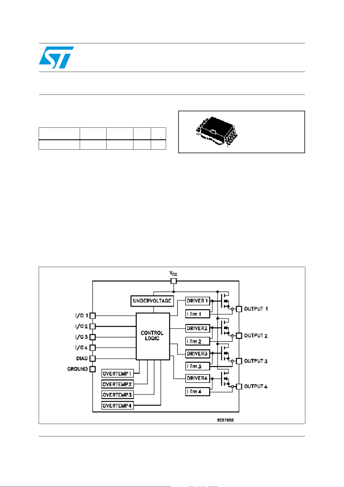
Figure 1. Block diagram
demag
(1)
R
DS(on)
(1)
I
out
(1)
V
CC
PowerSO-10
TM
Description
The VN340SP-33-E is a monolithic device made
using STMicroelectronics VIPower technology,
intended for driving four independent resistive or
inductive loads with one side connected to
ground. Active current limitation avoids dropping
the system power supply in case of shorted load.
Built-in thermal shut-down protects the chip from
overtemperature and short circuit. The open drain
diagnostic output indicates overtemperature
conditions. Each I/O is pulled down when
overtemperature condition of the relative channel
is verified.
August 2008 Rev 3 1/16
www.st.com
16
Page 2

Contents VN340SP-33-E
Contents
1 Maximum ratings . . . . . . . . . . . . . . . . . . . . . . . . . . . . . . . . . . . . . . . . . . . . 3
2 Pin connections . . . . . . . . . . . . . . . . . . . . . . . . . . . . . . . . . . . . . . . . . . . . . 4
3 Electrical characteristics . . . . . . . . . . . . . . . . . . . . . . . . . . . . . . . . . . . . . 5
4 Test circuits . . . . . . . . . . . . . . . . . . . . . . . . . . . . . . . . . . . . . . . . . . . . . . . . 7
5 Switching time waveforms and truth table . . . . . . . . . . . . . . . . . . . . . . . 9
6 Package mechanical data . . . . . . . . . . . . . . . . . . . . . . . . . . . . . . . . . . . . 11
7 Order codes . . . . . . . . . . . . . . . . . . . . . . . . . . . . . . . . . . . . . . . . . . . . . . . 14
8 Revision history . . . . . . . . . . . . . . . . . . . . . . . . . . . . . . . . . . . . . . . . . . . 15
2/16
Page 3
VN340SP-33-E Maximum ratings
1 Maximum ratings
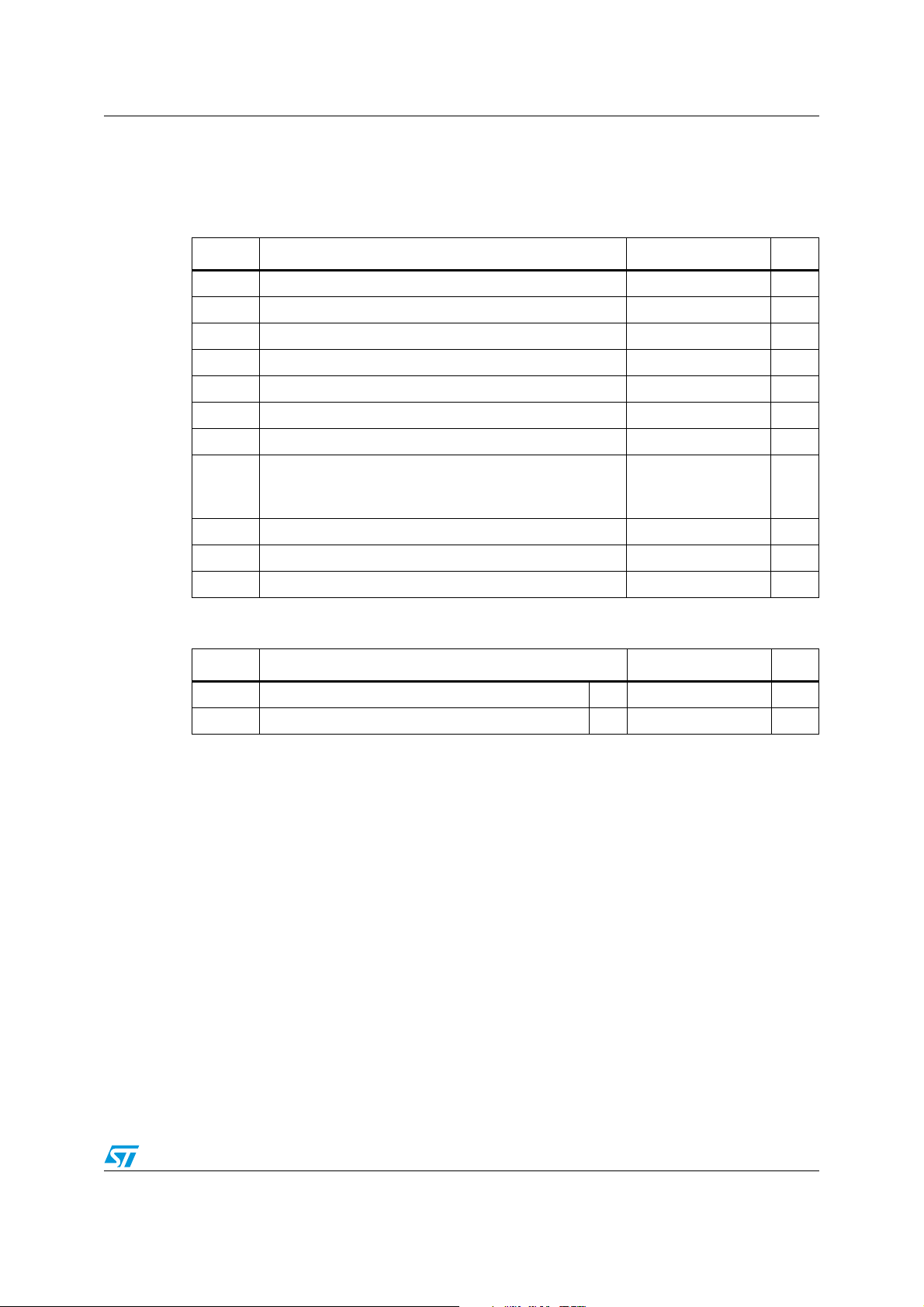
Table 1. Absolute maximum rating
Symbol Parameter Values Unit
V
-V
I
OUT
I
I
DIAG
V
ESD
Power supply voltage 45 V
CC
Reverse supply voltage -4 V
CC
Output current (continuos) Internally limited A
I
Reverse output current (per channel) -6 A
R
Input current (per channel) ± 10 mA
IN
Diag pin current ± 10 mA
Electrostatic discharge (R = 1.5 kΩ; C = 100 pF) 2000 V
Single pulse avalanche energy per channel not
AS
simultaneously
400 mJ
E
Figure 4.
Power dissipation at Tc = 25 °C Internally limited w
tot
Junction operating temperature Internally limited °C
J
Storage temperature -55 to 150 °C
T
P
T
STG
Table 2. Thermal data
Symbol Parameter Values Unit
R
R
1. Per channel
2. When mounted using minimum recommended pad size on FR-4 board
Thermal resistance junction-case
thJC
Thermal resistance junction-ambient
thJA
(1)
(2)
Max 3 °C/W
Max 50 °C/W
3/16
Page 4
Pin connections VN340SP-33-E
2 Pin connections
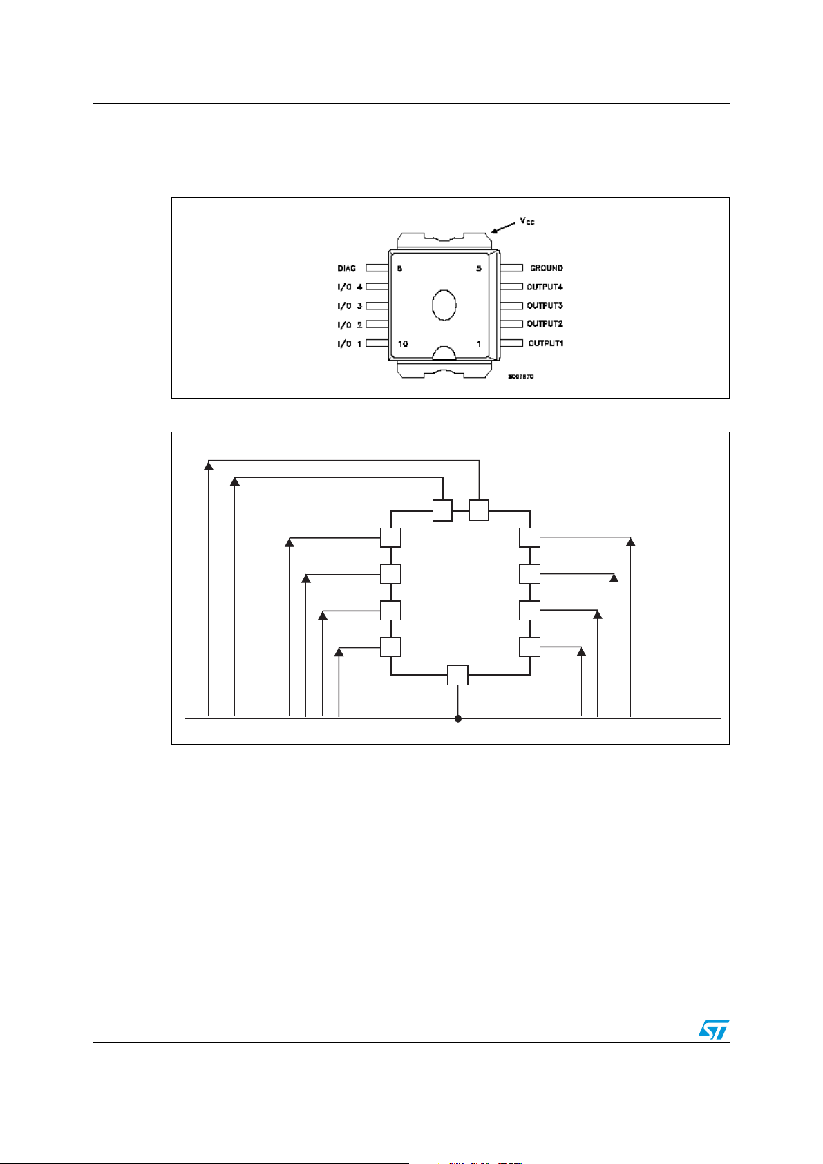
Figure 2. Connection diagram (top view)
Figure 3. Current and voltage conventions
VCC
VIN1
VIN2
VIN3
VIN4
IIN1
IIN2
IIN3
IIN4
IDIAG
VDIAG
9
8
7
6
IN2
IN3
IN4
DIAG
10
IN1
GND
V
CC
11
IOUT1
OUT1
OUT2
OUT3
OUT4
5
1
2
3
4
IOUT2
IOUT3
IOUT4
VOUT1
VOUT2
VOUT3
VOUT4
4/16
Page 5
VN340SP-33-E Electrical characteristics
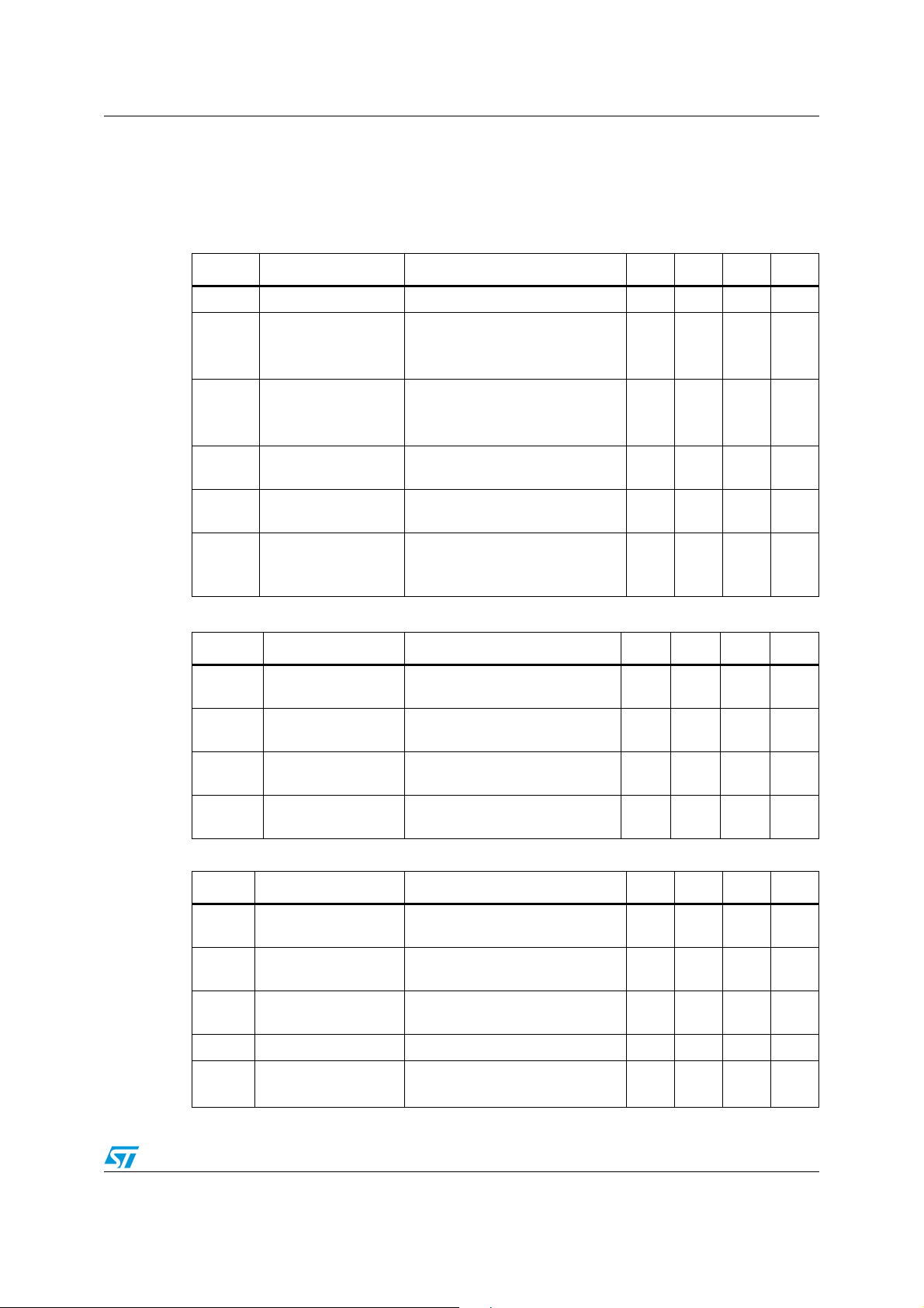
3 Electrical characteristics
10 V < V
Table 3. Power section
< 36 V; -40 °C < TJ < 125 °C; unless otherwise specified
CC
Symbol Parameter Test conditions Min Typ Max Unit
V
R
V
V
demag
I
LGND
Table 4. Switching (V
Supply voltage 10 36 V
CC
I
= 0.5 A; TJ = 25 °C
OUT
On state resistance
ON
I
= 0.5 A; TJ = 85 °C
OUT
= 0.5 A; TJ = 125 °C
I
OUT
All channels OFF
I
Supply current
S
Low state output
OL
voltage
Output voltage at
turn-off
Output current at
turn-off
CC
On state; V
= 125 °C)
(T
J
V
= VIL; R
IN
I
= 0.5 A; L
OUT
VCC = V
V
= 18 to 30 V
STAT
= - 25 °C to 85 °C Figure 6.
T
A
INn
= 30 V; I
IN
>= 10 MΩ 1.5 V
LOAD
LOAD
= V
GND
= 24 V)
OUT
>= 1 mH
=
= 0 V
-65VCC-55VCC-
V
CC
0.2
0.32
0.4
1
6
45
2mA
Symbol Parameter Test conditions Min Typ Max Unit
Ω
Ω
Ω
mA
mA
V
t
d(ON)
t
d(OFF)
Table 5. Logical input
Turn-on delay time of
Output current
Rise time of output
t
r
current
Turn-off delay time of
output current
Fall time of output
t
f
current
I
= 0.5 A, resistive load input
OUT
rise time < 0.1 μs, T
I
= 0.5 A, resistive load input
OUT
rise time < 0.1 μs, T
I
= 0.5 A, resistive load input
OUT
= 25 °C
J
= 25 °C
J
rise time < 0.1 μs, TJ = 25 °C
I
= 0.5 A, resistive load input
OUT
rise time < 0.1 μs, T
= 25 °C
J
52 100 μs
94 250 μs
34 50 μs
820μs
Symbol Parameter Test conditions Min Typ Max Unit
I/O input low level
V
IL
voltage
I/O input high level
V
IH
voltage
V
I(HYST)
V
1. The input voltage is internally clamped at 32 V minimum, it is possible to connect the input pins to an higher
I/O input hysteresis
voltage
I/O input current V
I
IN
I/O input clamp
ICL
voltage
voltage via an external resistor calculate to not exceed 10 mA
(1)
(1)
= 30 V 25 μΑ
IN
I
= 1 mA
IN
I
= -1 mA
IN
3.5 V
0.5 V
32 36
-0.7
2V
V
V
5/16
Page 6
Electrical characteristics VN340SP-33-E
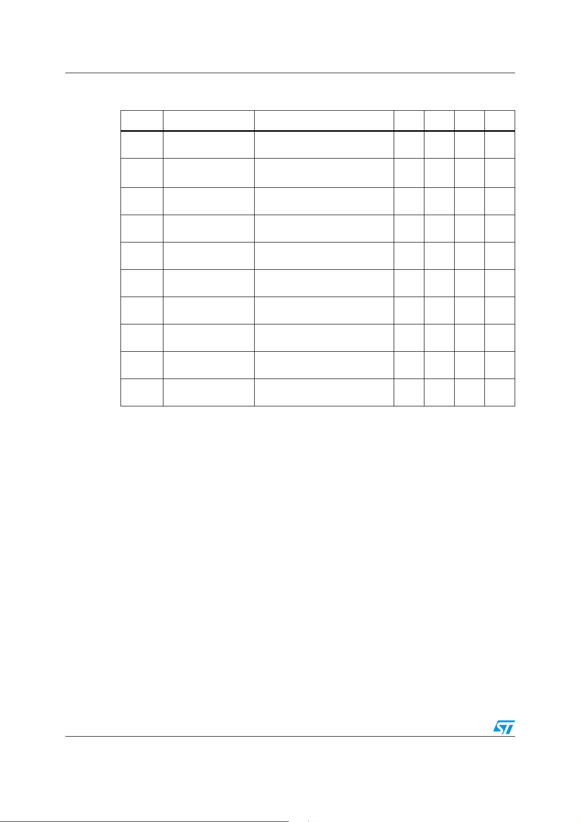
Table 6. Protection and diagnostic
Symbol Parameter Test conditions Min Typ Max Unit
Status voltage output
V
DIAG
V
SCL
V
I
OVPK
I
DIAGH
USD
I
LIM
(1)
low
(1)
Status clamp voltage
Undervoltage shut
down
DC Short circuit
current
Peak short circuit
current
Leakage ondiag pin in
high state
I
= 5 mA (Fault condition) 1 V
DIAG
I
DIAG
I
DIAG
= 1 mA
= 1 mA
32 36
-0.7
58V
= 24 V; R
V
CC
V
= 24 V; VIN = 30 V;
CC
R
< 10 mΩ
LOAD
= 24 V 25 μΑ
V
DIAG
< 10 mΩ 12A
LOAD
V
V
4A
I
LOAD
t
T
1. Status determination > 100 μs after the switching edge.
Output leakage
current
Delay time of current
SC
limiter
Thermal shut down
TSD
temperature
Thermal reset
T
R
temperature
= 10 to 36 V; VIN = V
V
CC
IL
50 μΑ
100 μs
150 170 °C
135 155 °C
Note: If INPUT pin is floating the corresponding channel will automatically switch OFF. If GND pin
is disconnected, the channel will switch OFF provided V
not exceed 36 V.
CC
6/16
Page 7
VN340SP-33-E Test circuits
4 Test circuits
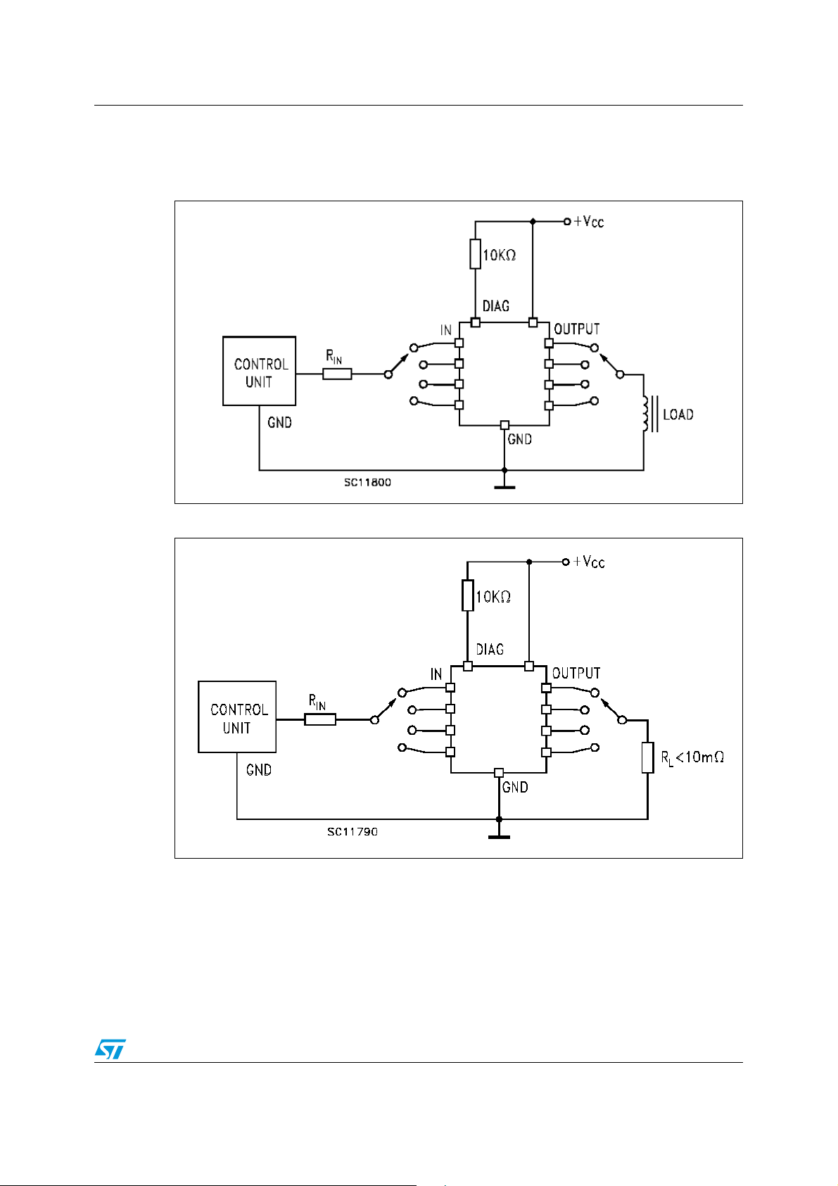
Figure 4. Avalance energy test circuit
Figure 5. Peak short circuit test diagram
7/16
Page 8
Test circuits VN340SP-33-E
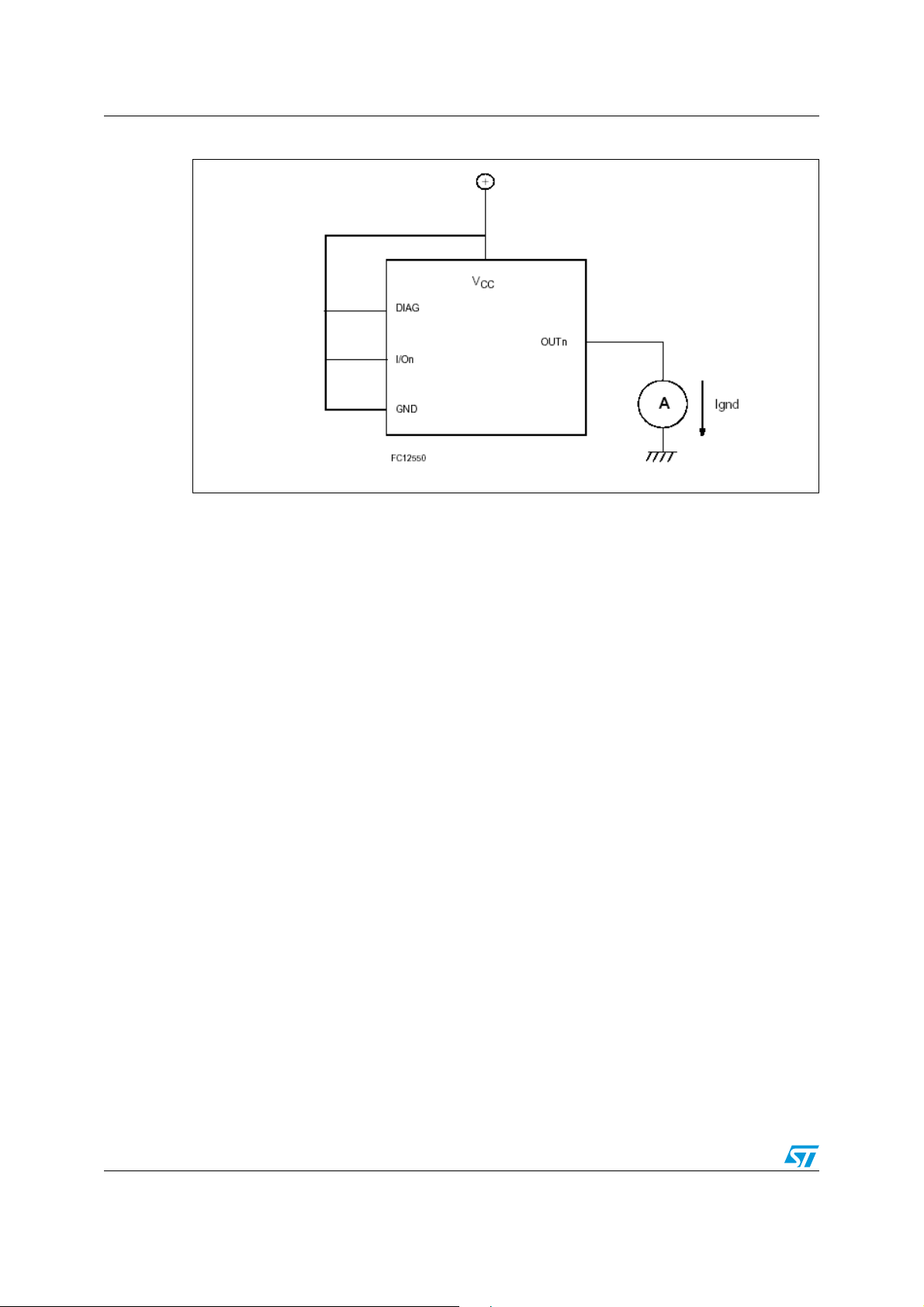
Figure 6. I
test configuration
LGND
8/16
Page 9
VN340SP-33-E Switching time waveforms and truth table
5 Switching time waveforms and truth table
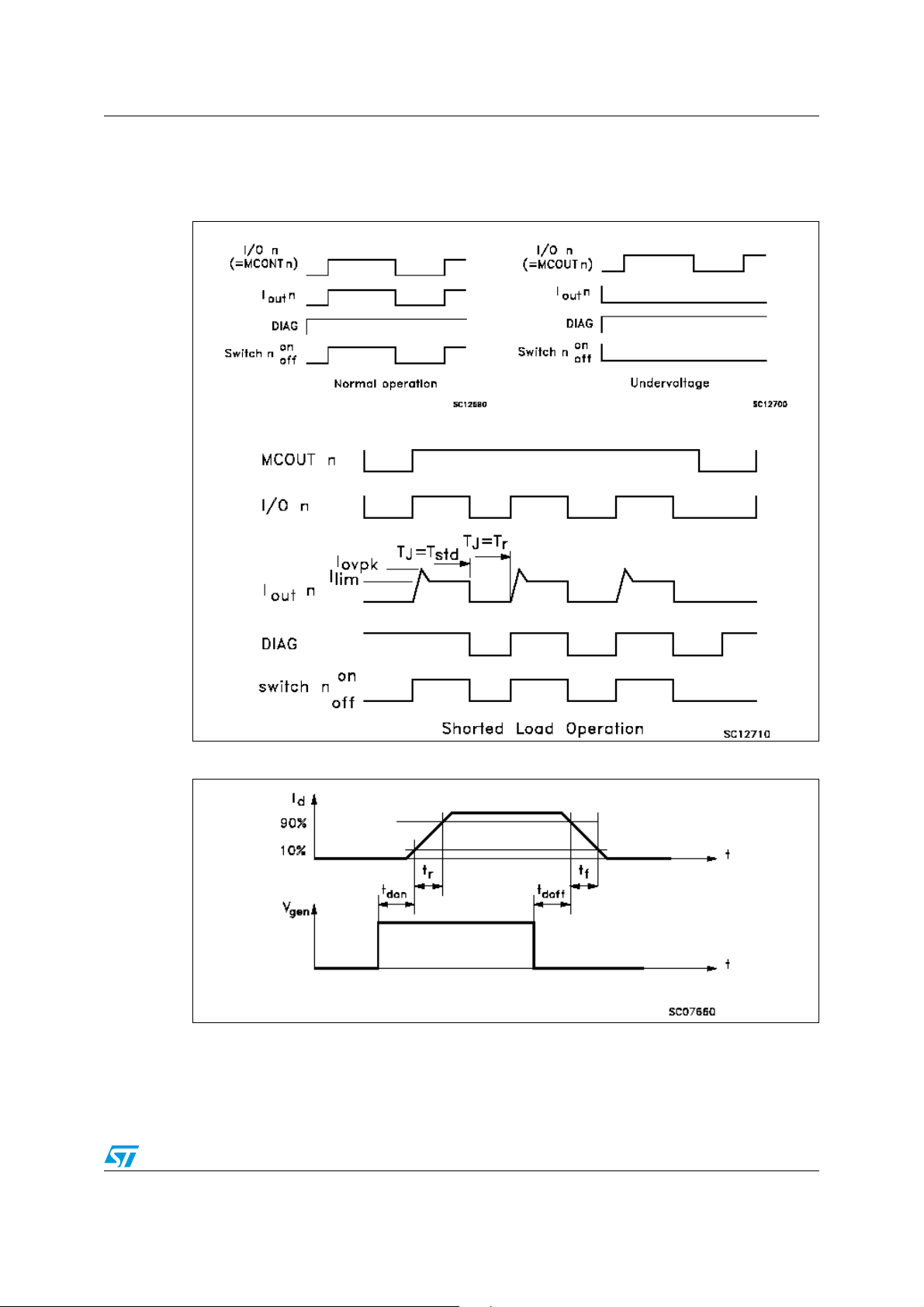
Figure 7. Switching waveforms
Figure 8. Switching parameter test conditions
9/16
Page 10
Switching time waveforms and truth table VN340SP-33-E
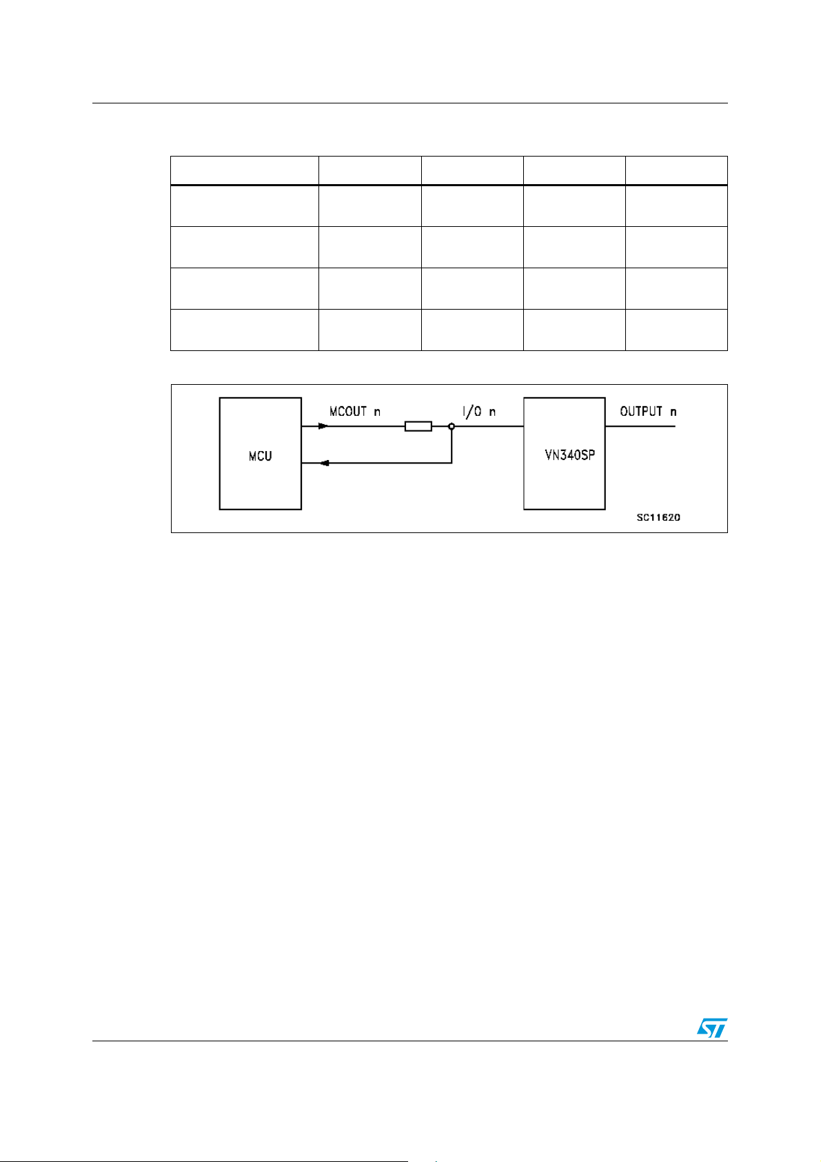
Table 7. Truth table
MCOUTn I/On OUTPUTn Diagnostic
Normal operation
Overtemperature
Undervoltage
Shorted load
(Current limitation)
Figure 9. Driving circuit
L
H
L
H
L
H
L
H
L
H
L
L
L
H
L
H
L
H
L
L
L
L
L
H
H
H
H
L
H
H
H
H
10/16
Page 11

VN340SP-33-E Package mechanical data
6 Package mechanical data
In order to meet environmental requirements, ST offers these devices in ECOPACK®
packages. These packages have a lead-free second level interconnect. The category of
second level interconnect is marked on the package and on the inner box label, in
compliance with JEDEC Standard JESD97. The maximum ratings related to soldering
conditions are also marked on the inner box label. ECOPACK is an ST trademark.
ECOPACK specifications are available at: www.st.com
11/16
Page 12
Package mechanical data VN340SP-33-E
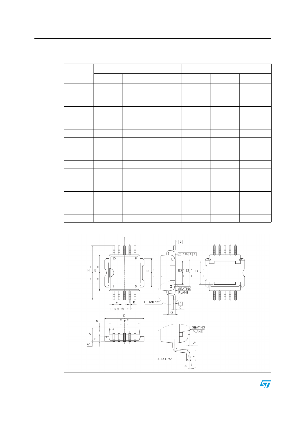
Table 8. PowerSO-10 mechanical data
Dim
Min Typ Max Min Typ Max
A 3.35 3.65 0.132 0.144
A1 0.00 0.10 0.000 0.004
B 0.40 0.60 0.016 0.024
c 0.23 0.32 0.009 0.012
D 9.40 9.60 0.370 0.378
D1 7.40 7.60 0.291 0.300
E 9.30 9.50 0.366 0.374
E1 7.20 7.40 0.283 0.291
E2 7.20 7.60 0.283 0.300
E3 6.10 6.35 0.240 0.250
E4 5.90 6.10 0.232 0.240
e 1.27 0.050
F 1.25 1.35 0.049 0.053
H 13.80 14.40 0.543 0.567
h 0.50 0.002
L 1.20 1.80 0.047 0.071
q 1.70 0.067
a 0° 8°
Mm Inch
Figure 10. Package dimension
12/16
Page 13
VN340SP-33-E Package mechanical data
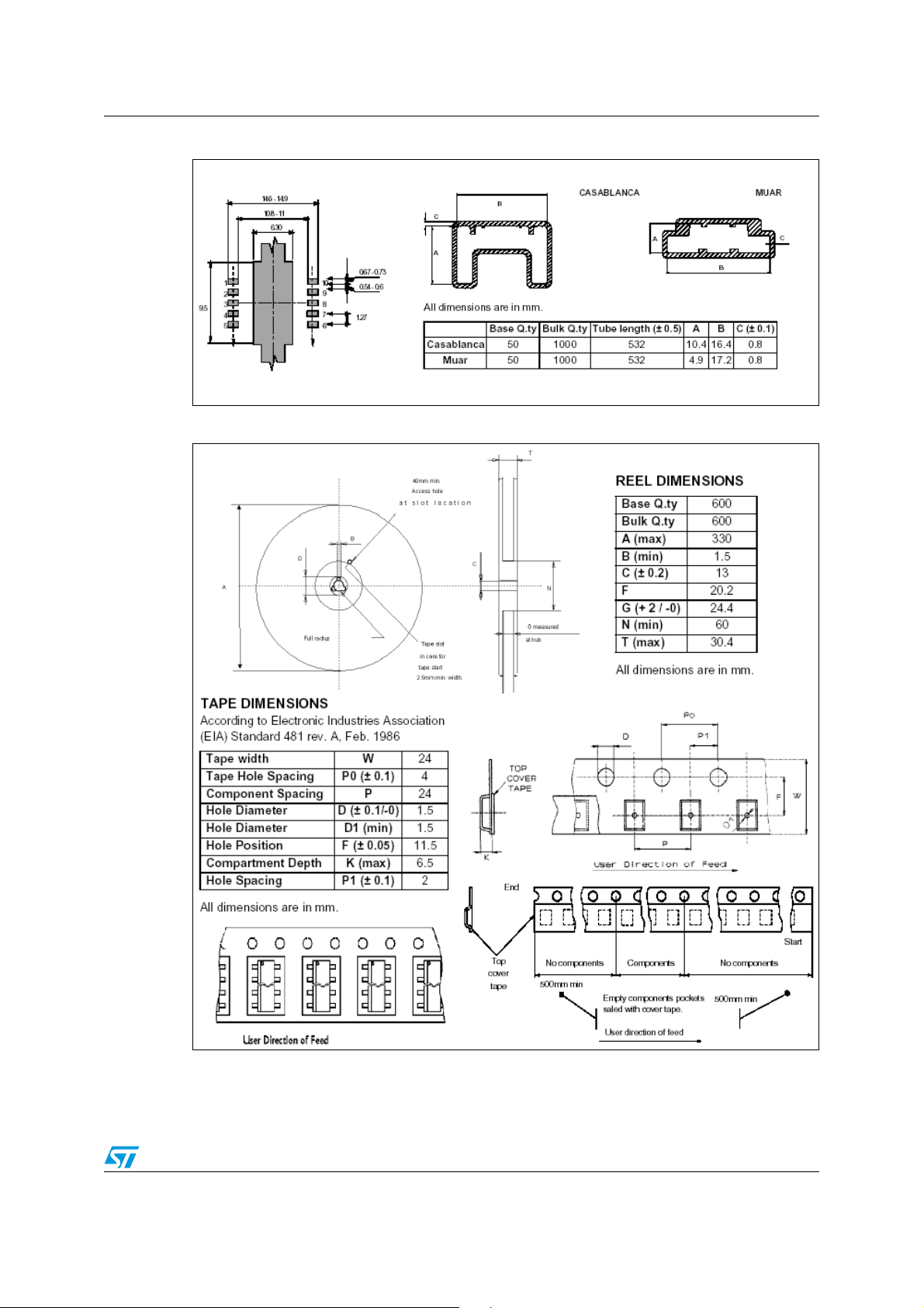
Figure 11. PowerSO-10TM suggested pad and tube shipment (No suffix)
Figure 12. Tape and reel shipment (Suffix “TR“)
13/16
Page 14
Order codes VN340SP-33-E
7 Order codes
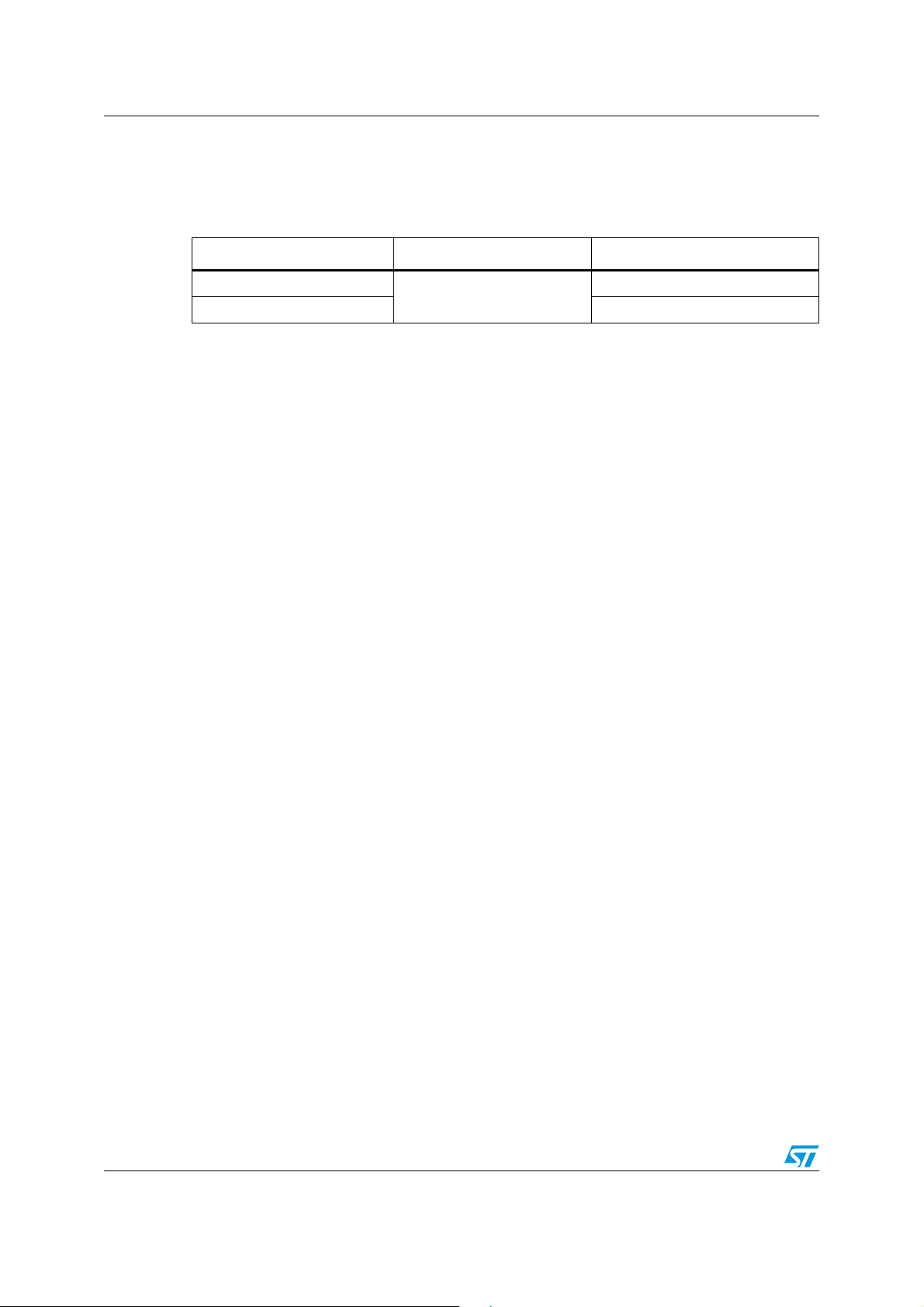
Table 9. Order codes
Order codes Package Packaging
VN340SP-33-E
PowerSO-10
VN340SPTR-33-E Tape and reel
TM
Tu b e
14/16
Page 15
VN340SP-33-E Revision history
8 Revision history
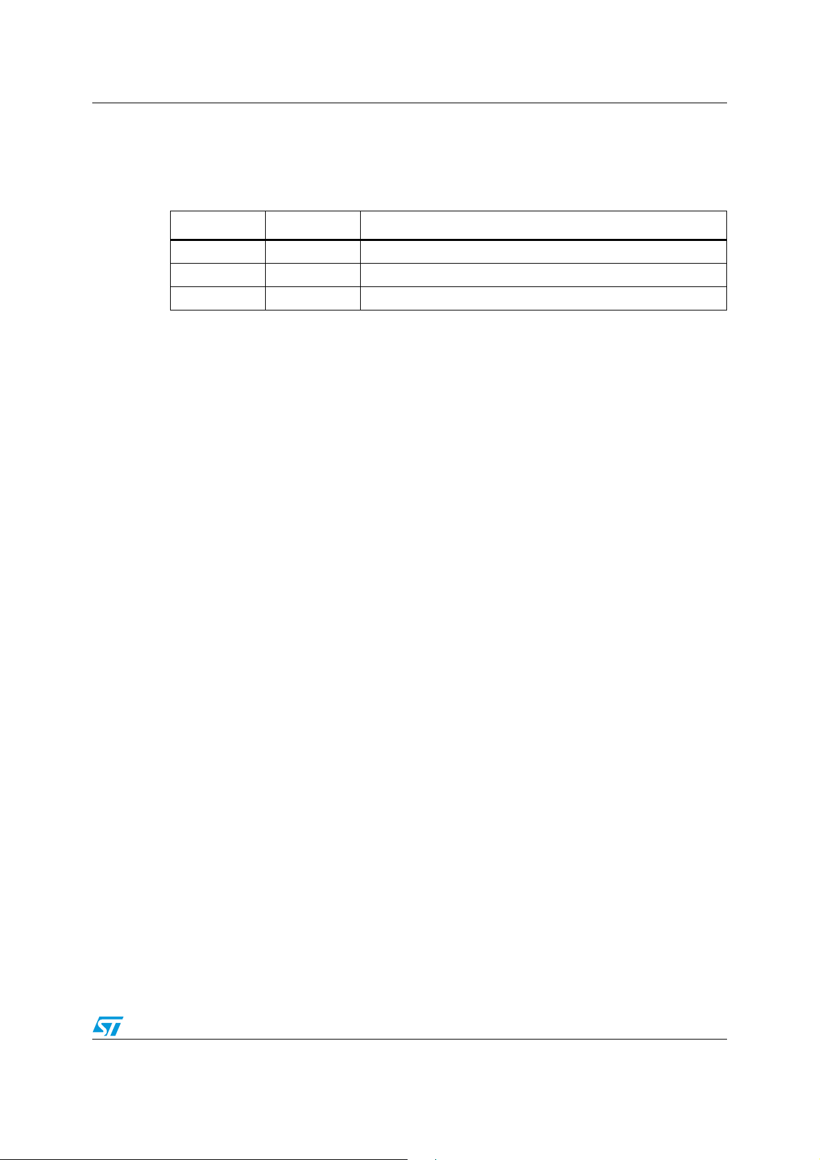
Table 10. Document revision history
Date Revision Changes
5-Sep-2005 1 Final release
19-Mar-2007 2 Document reformatted, typo in Note 1 on page 6
22-Aug-2008 3 Updated Ta bl e 9
15/16
Page 16

VN340SP-33-E
Please Read Carefully:
Information in this document is provided solely in connection with ST products. STMicroelectronics NV and its subsidiaries (“ST”) reserve the
right to make changes, corrections, modifications or improvements, to this document, and the products and services described herein at any
time, without notice.
All ST products are sold pursuant to ST’s terms and conditions of sale.
Purchasers are solely responsible for the choice, selection and use of the ST products and services described herein, and ST assumes no
liability whatsoever relating to the choice, selection or use of the ST products and services described herein.
No license, express or implied, by estoppel or otherwise, to any intellectual property rights is granted under this document. If any part of this
document refers to any third party products or services it shall not be deemed a license grant by ST for the use of such third party products
or services, or any intellectual property contained therein or considered as a warranty covering the use in any manner whatsoever of such
third party products or services or any intellectual property contained therein.
UNLESS OTHERWISE SET FORTH IN ST’S TERMS AND CONDITIONS OF SALE ST DISCLAIMS ANY EXPRESS OR IMPLIED
WARRANTY WITH RESPECT TO THE USE AND/OR SALE OF ST PRODUCTS INCLUDING WITHOUT LIMITATION IMPLIED
WARRANTIES OF MERCHANTABILITY, FITNESS FOR A PARTICULAR PURPOSE (AND THEIR EQUIVALENTS UNDER THE LAWS
OF ANY JURISDICTION), OR INFRINGEMENT OF ANY PATENT, COPYRIGHT OR OTHER INTELLECTUAL PROPERTY RIGHT.
UNLESS EXPRESSLY APPROVED IN WRITING BY AN AUTHORIZED ST REPRESENTATIVE, ST PRODUCTS ARE NOT
RECOMMENDED, AUTHORIZED OR WARRANTED FOR USE IN MILITARY, AIR CRAFT, SPACE, LIFE SAVING, OR LIFE SUSTAINING
APPLICATIONS, NOR IN PRODUCTS OR SYSTEMS WHERE FAILURE OR MALFUNCTION MAY RESULT IN PERSONAL INJURY,
DEATH, OR SEVERE PROPERTY OR ENVIRONMENTAL DAMAGE. ST PRODUCTS WHICH ARE NOT SPECIFIED AS "AUTOMOTIVE
GRADE" MAY ONLY BE USED IN AUTOMOTIVE APPLICATIONS AT USER’S OWN RISK.
Resale of ST products with provisions different from the statements and/or technical features set forth in this document shall immediately void
any warranty granted by ST for the ST product or service described herein and shall not create or extend in any manner whatsoever, any
liability of ST.
ST and the ST logo are trademarks or registered trademarks of ST in various countries.
Information in this document supersedes and replaces all information previously supplied.
The ST logo is a registered trademark of STMicroelectronics. All other names are the property of their respective owners.
© 22 STMicroelectronics - All rights reserved
STMicroelectronics group of companies
Australia - Belgium - Brazil - Canada - China - Czech Republic - Finland - France - Germany - Hong Kong - India - Israel - Italy - Japan -
Malaysia - Malta - Morocco - Singapore - Spain - Sweden - Switzerland - United Kingdom - United States of America
www.st.com
16/16
 Loading...