

Page 1
VN06SP
HIGH SIDE SMART POWER SOLID STATE RELAY
July 1998
TYPE V
DSS
R
DS(on)
I
n(*)
V
CC
VN06SP 60 V 0.18 Ω 1.9 A 26 V
■ MAXIMUM CONTINUOUS OUTPUT
CURRENT (#):9 A @ T
c
=85oC
■ 5 V LOGIC LEVEL COMPATIBLE INPUT
■ THERMAL SHUT-DOWN
■ UNDER VOLTAG E PROT E CT ION
■ OPEN DRAIN DIAGNOSTIC OUTPUT
■ INDUCTIVE LOAD FAST
DEMAGNETIZATION
■ VERY LOW STAND-BY POWER
DISSIPATION
DESCRIP TION
The VN06SP is a monolithic device made using
STMicroelectronics VIPower Technology,
intended for driving resistive or inductive loads
with one side grounded.
Built-in thermal shut-down protects the chip from
over temperature and short circ uit.
The open drain diagnostic output indicates: open
load in off state, and in on state, output shorted to
V
CC
and overtemperature. Fast demagnetization
of inductive loads is archivied by negative (-18V)
load voltage at turn-off.
®
1
10
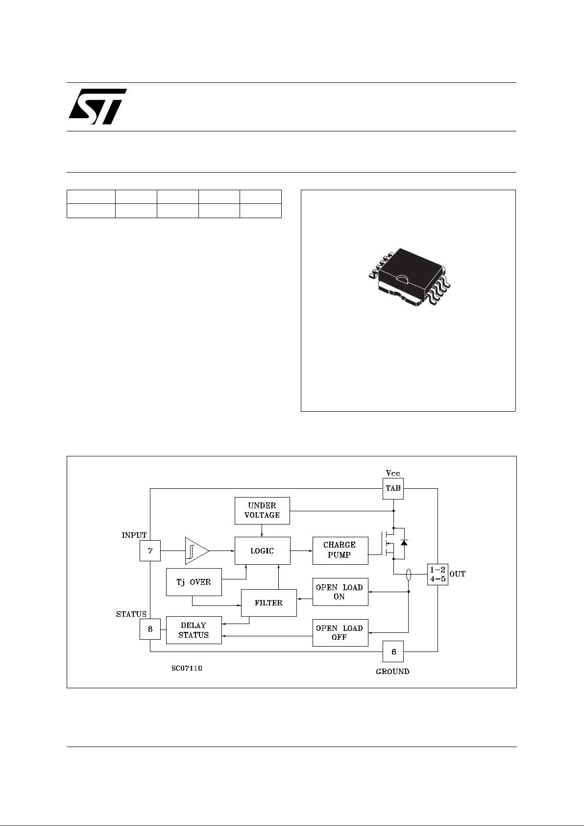
Powe r SO-10
(*) In = Nominal current according to ISO definition for high side automotive switch (see note 1)
(#) The maximum continuous output current is the the current at T
c
= 85 oC for a battery voltage of 13V which does not activate self
protection.
1/9
Page 2
ABSOLUTE MAXIMUM RATING
Symbol Parameter Value Unit
V
(BR)DSS
Drain-Source Breakdown Voltage 60 V
I
OUT
Output Current (cont.) at Tc = 85 oC9A
I
R
Reverse Output Current at Tc = 85 oC-9A
I
IN
Input Current ±10 mA
-V
CC
Reverse Supply Voltage -4 V
I
STAT
Status Current ±10 mA
V
ESD
Electrostatic Discharge (1.5 kΩ, 100 pF) 2000 V
P
tot
Power Dissipation at Tc = 85 oC 27 W
T
j
Junction Operating Temperature -40 to 150
o
C
T
stg
Storage Temperature -55 to 150
o
C
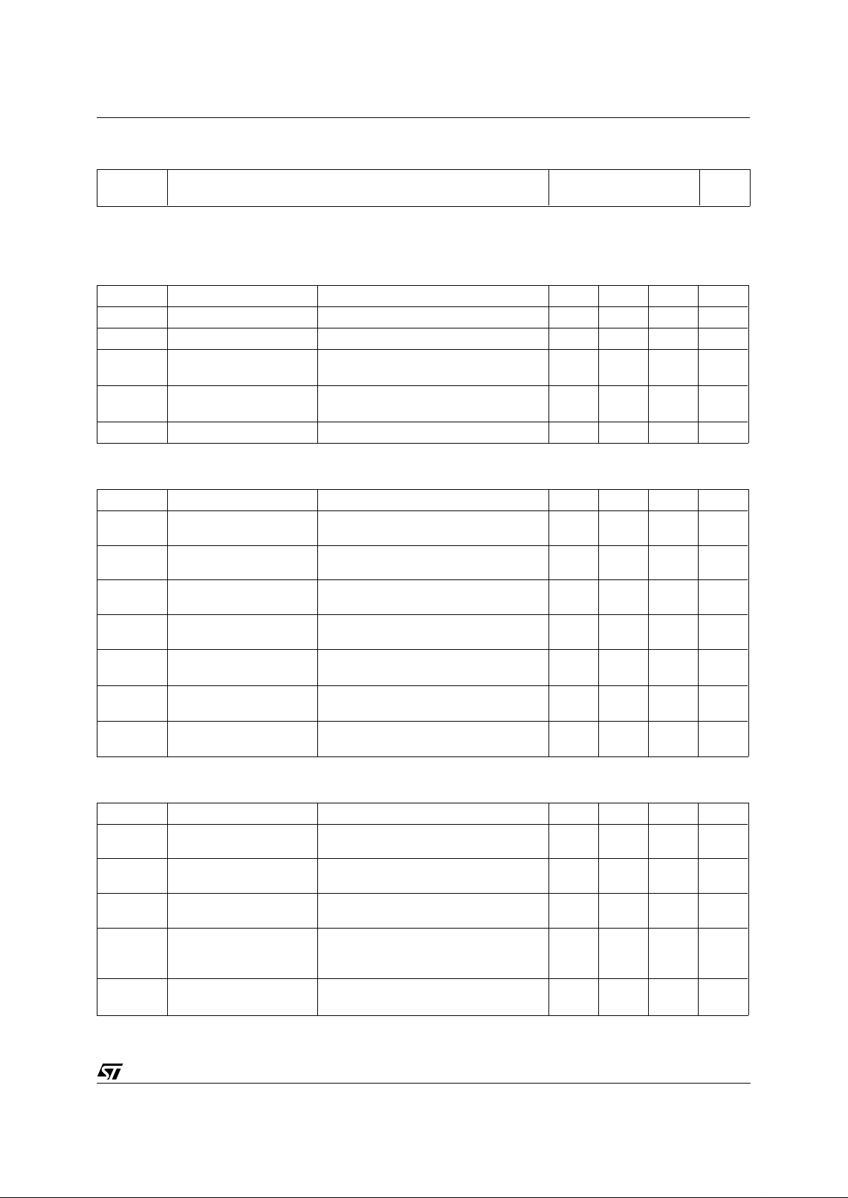
CONNECTION DIAGRAMS
CURRENT AND VOLTAGE CONVENTI ONS
VN06SP
2/9
Page 3
THERMAL DATA
R
thj-case
R
thj-amb
Thermal Resistance Junction-case Max
Thermal Resistance Junction-ambient Max
2.4
50
o
C/W
o
C/W
When mounted using minimum recommended pad size on FR-4 board
ELECTRICAL CHARACTERISTICS (VCC = 13 V; -40 ≤ Tj ≤ 125 oC unless otherwise specified)
POWER
Symbol Parameter Test Conditions Min. Typ. Max. Unit
V
CC
Supply Voltage 5.5 13 26 V
In(*) Nominal Current Tc = 85 oC V
DS(on)
≤ 0.5 (note 1) 1.9 A
R
on
On State Resistance I
OUT
= 1.9 A
I
OUT
= 1.9 A Tj = 25 oC
0.36
0.18
Ω
Ω
I
S
Supply Current Off State Tj ≥ 25 oC
On State
50
15
µA
mA
V
DS(MAX)
Maximum Voltage Drop I
OUT
= 8.5 A Tc = 85 oC 2.75 V
SWITCHING
Symbol Parameter Test Conditions Min. Typ. Max. Unit
t
d(on)
(^) Turn-on Delay Time Of
Output Current
I
OUT
= 1.9 A Resistive Load
Input Rise Time < 0.1 µs
20 µs
t
r
(^) Rise Time Of Output
Current
I
OUT
= 1.9 A Resistive Load
Input Rise Time < 0.1 µs
20 µs
t
d(off)
(^) Turn-off Delay Time Of
Output Current
I
OUT
= 1.9 A Resistive Load
Input Rise Time < 0.1 µs
25 µs
t
f
(^) Fall Time Of Output
Current
I
OUT
= 1.9 A Resistive Load
Input Rise Time < 0.1 µs
6 µs
(di/dt)
on
Turn-on Current Slope I
OUT
= 1.9 A
I
OUT
= IOV
0.08 0.51A/µs
A/µs
(di/dt)
off
Turn-off Current Slope I
OUT
= 1.9 A
I
OUT
= I
OV
0.2 3
3
A/µs
A/µs
V
demag
Inductive Load Clamp
Voltage
I
OUT
= 1.9 A L = 1 mH -24 -18 -14 V
LOGIC INP UT
Symbol Parameter Test Conditions Min. Typ. Max. Unit
V
IL
Input Low Level
Voltage
0.8 V
V
IH
Input High Level
Voltage
2(•)V
V
I(hyst.)
Input Hysteresis
Voltage
0.5 V
I
IN
Input Current VIN = 5 V
V
IN
= 2 V
V
IN
= 0.8 V 25
250 500
250
µA
µA
µA
V
ICL
Input Clamp Voltage IIN = 10 mA
I
IN
= -10 mA
5.5 6
-0.7 -0.3
V
V
VN06SP
3/9
Page 4

ELECTRICAL CHARACTERISTICS (continued)
PROTECT IO N AND DIAG NO S TIC S
Symbol Parameter Test Conditions Min. Typ. Max. Unit
V
STAT
Status Voltage Output
Low
I
STAT
= 1.6 mA 0.4 V
V
USD
Under Voltage Shut
Down
5V
V
SCL
Status Clamp Voltage I
STAT
= 10 mA
I
STAT
= -10 mA
6
-0.7
V
V
I
OV
Over Current R
LOAD
< 10 mΩ -40 Tc 125 oC60A
I
AV
Average Current in
Short Circuit
R
LOAD
< 10 mΩ Tc = 85 oC 1.4 A
I
OL
Open Load Current
Level
5 80 180 mA
T
TSD
Thermal Shut-down
Temperature
140
o
C
T
R
Reset Temperature 125
o
C
V
OL
Open Load Voltage
Level
Off-State (note 2) 2.5 3.75 5 V
t
1(on)
Open Load Filtering
Time
(note 3) 1 5 10 ms
t
1(off)
Open Load Filtering
Time
(note 3) 1 5 10 ms
t
2(off)
Open Load Filtering
Time
(note 3) 1 5 10 ms
t
povl
Status Delay (note 3) 5 10 µs
t
pol
Status Delay (note 3) 50 700 µs
(^) See Switchig Time Waveforms
() The V
IH
is internally clamped at 6V about. It is possible to connect this pin to an higher voltage via an external resistor calculat ed to not
exceed 10 mA at the input pin.
note 1:The Nominal Current is the current at T
c
= 85 oC for battery voltage of 13V which produces a voltage drop of 0.5 V
note 2:I
OL(off)
= (VCC -VOL)/ROL (see figure)
note 3:t
1(on)
: minimum open load duration which acctivates the status output
t
1(off)
: minimum load recovery time which desactivates the status output
t
2(off)
: minimum on time after thermal shut down which desactivates status output
t
povl tpol
: ISO definition (see figure).
Note 2 Relevant Figure Not e 3 Relevant Figure
VN06SP
4/9
Page 5

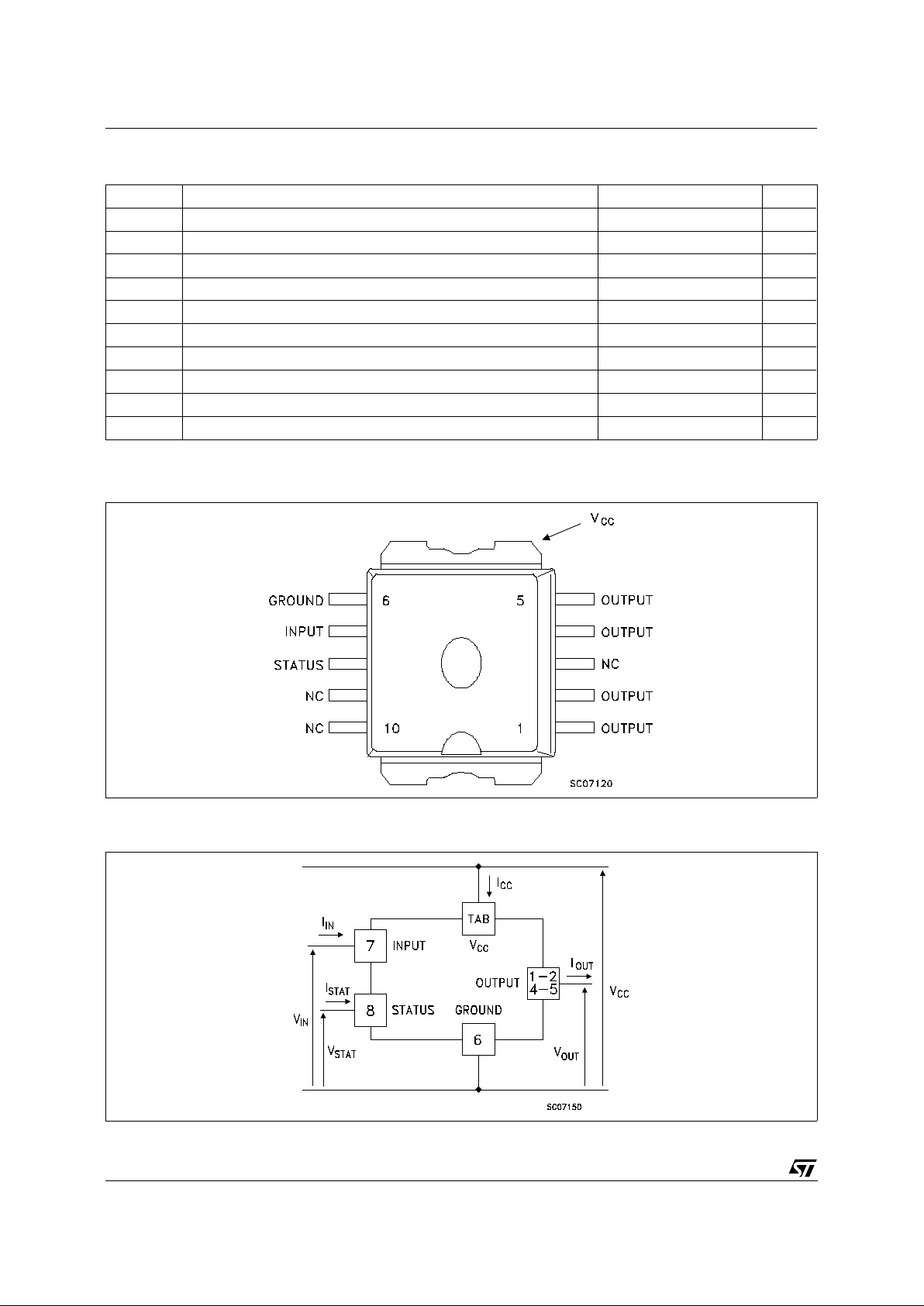
FUNCTIONAL DESCRI PT ION
The device has a diagnostic output which
indicates open load conditions in off state as well
as in on state, output shorted to V
CC
and
overtemperature. The truth table shows input,
diagnostic and output voltage level in normal
operation and in fault conditions. The output
signals are processed by internal logic. The
open load diagnostic output has a 5 ms filtering.
The filter gives a continuous signal for the fault
condition after an initial delay of about 5 ms. This
means that a disconnection during normal
operation, with a duration of less than 5 ms does
not affect the status output. Equally, any
re-connection of less than 5 ms during a
disconnection duration does not affect the status
output. No delay occur for the status to go low in
case of overtemperature conditions. From the
falling edge of the input signal the status output
initially low in fault condition (over temperature or
open load) will go back with a delay (t
povl
)in case
of overtemperature condition and a delay (t
pol
) in
case of open load. These feature fully comply
with International Standard Office (I.S.O.)
requirement for automotive High Side Driver.
To protect the device against short circuit and
over current conditions, the thermal protection
turns the integrated Power MOS off at a
minimum junction temperature of 140
o
C.
When the temperature returns to 125
o
C the
switch is automatically turned on again. In short
circuit the protection reacts with virtually no
delay, the sensor being located in the region of
the die where the heat is generated. Driving
inductive loads, an internal function of the
device ensures the fast demagnetization with a
typical voltage (V
demag
) of -18V.
This function allows to greatly reduce the power
dissipation according to the formula:
P
dem
= 0.5 • L
load
• (I
load
)2• [(VCC+V
demag
)/V
demag
]
•f
where f = switching frequency and
V
demag
= demagnetization voltage
Based on this formula it is possible to know
the value of inductance and/or current to avoid
a thermal shut-down. The maximum inductance
which causes the chip temperature to reach the
shut down temperature in a specific thermal
environment, is infact a function of the load
current for a fixed V
CC
, V
demag
and f.
PROTECTING THE DEVICE AGAIST LOAD
DUMP - TEST PULSE 5
The device is able to withstand the test pulse
No. 5 at level II (V
s
= 46.5V) according to the
ISO T/R 7637/1 without any external
component. This means that all functions of the
device are performed as designed after
exposure to disturbance at level II. The VN06SP
is able to withstand the test pulse No.5 at level
III adding an external resistor of 150 ohm
between GND pin and ground plus a filter
capacitor of 1000 µF between V
CC
pin and
ground (if R
LOAD
≤ 20 Ω).
PROTECTING THE DEVICE AGAINST
REVERSE BATTERY
The simplest way to protect the device against a
continuous reverse battery voltage (-26V) is to
insert a Schottky diode between GND pin and
ground, as shown in the typical application circuit
(fig.3).
The consequences of the voltage drop across
this diode are as follows:
If the input is pulled to power GND, a negative
voltage of -V
f
is seen by the device. (Vil, Vih
thresholds and Vstat are increased by Vf with
respect to power GND).
The undervoltage shutdown level is increa- sed
by Vf.
If there is no need for the control unit to handle
external analog signals referred to the power
GND, the best approach is to connect the
reference potential of the control unit to node [6]
(see application circuit in fig. 4), which becomes
the common signal GND for the whole control
board avoiding shift of V
ih
, Vil and V
stat
. This
solution allows the use of a standard diode.
Switching Ti me Waveforms
VN06SP
5/9
Page 6

TRUTH TABLE
INPUT OUTPUT DIAGNOSTIC
Normal Operation L
H
L
H
H
H
Open Circuit (No Load) H H L
Over-temperature H L L
Under-voltage X L H
Short load to V
CC
LHL
Figure 1: Waveforms
Figure 2: Over Current Test Circuit
VN06SP
6/9
Page 7

Figure 3: Typical Application Circuit With A Schott ky Diode For Reverse Supply Prot ection
Figure 4: Typical Application Circuit With Separ ate Signal Gr ound
VN06SP
7/9
Page 8

DIM.
mm inch
MIN. TYP. MAX. MIN. TYP. MAX.
A 3.35 3.65 0.132 0.144
A1 0.00 0.10 0.000 0.004
B 0.40 0.60 0.016 0.024
c 0.35 0.55 0.013 0.022
D 9.40 9.60 0.370 0.378
D1 7.40 7.60 0.291 0.300
E 9.30 9.50 0.366 0.374
E1 7.20 7.40 0.283 0.291
E2 7.20 7.60 0.283 0.300
E3 6.10 6.35 0.240 0.250
E4 5.90 6.10 0.232 0.240
e1.27 0.050
F 1.25 1.35 0.049 0.053
H 13.80 14.40 0.543 0.567
h0.50 0.002
L 1.20 1.80 0.047 0.071
q1.70 0.067
α0
o
8
o
DETAIL "A"
PLANE
SEATING
α
L
A1
F
A1
h
A
D
D1
= =
= =
= =
E4
0.10
A
E1E3
C
Q
A
= =
B
B
DETAIL "A"
SEATING
PLANE
= =
= =
E2
610
51
e
B
HE
M
0.25
= =
= =
0068039-C
PowerSO-10 MECHANICAL DATA
VN06SP
8/9
Page 9

Information furnished is believed to be accurate and reliable. However, STMicroelectronics assumes no responsibility for the consequences
of use of such information n or for any infrin gement of patents or othe r rights of third parties which may result from its use. No licens e i s
granted by implication or otherwise under any patent or patent rights of STMicroelectronics. Specification mentioned in this publication are
subject to change without notice. This publication supersedes and replaces all information previously supplied. STMicroelectronics products
are not authorized for use as critical components in life support devices or systems without express written approval of STMicroelectronics.
The ST logo is a trademark of STMicroelectronics
© 1998 STMicroelectronics – Printed in Italy – All Rights Reserved
STMicroelectronics GROUP OF COMPANIES
Australia - Brazil - Canada - China - France - Germany - Italy - Japan - Korea - Malaysia - Malta - Mexico - Morocco - The Netherlands -
Singapore - Spain - Sweden - Switzerland - Taiwan - Thailand - United Kingdom - U.S.A.
.
VN06SP
9/9
 Loading...