

Page 1
VN05NSP
HIGH SIDE SMART POWER SOLID STATE RELAY
TYPE V
VN05 NS P 60 V 0.18 Ω 13 A 26 V
■ OUTPUTCURRENT(CONTINUOUS):
13 A @ T
■ 5 V LOGIC LEVEL COMPATIBLEINPUT
■ THERMALSHUT-DOWN
■ UNDERVOLTAGE SHUT-DOWN
■ OPENDRAIN DIAGNOSTIC OUTPUT
■ VERY LOW STAND-BY POWER
DSS
=25oC
c
R
DS(on)
I
OUT
V
CC
DISSIPATION
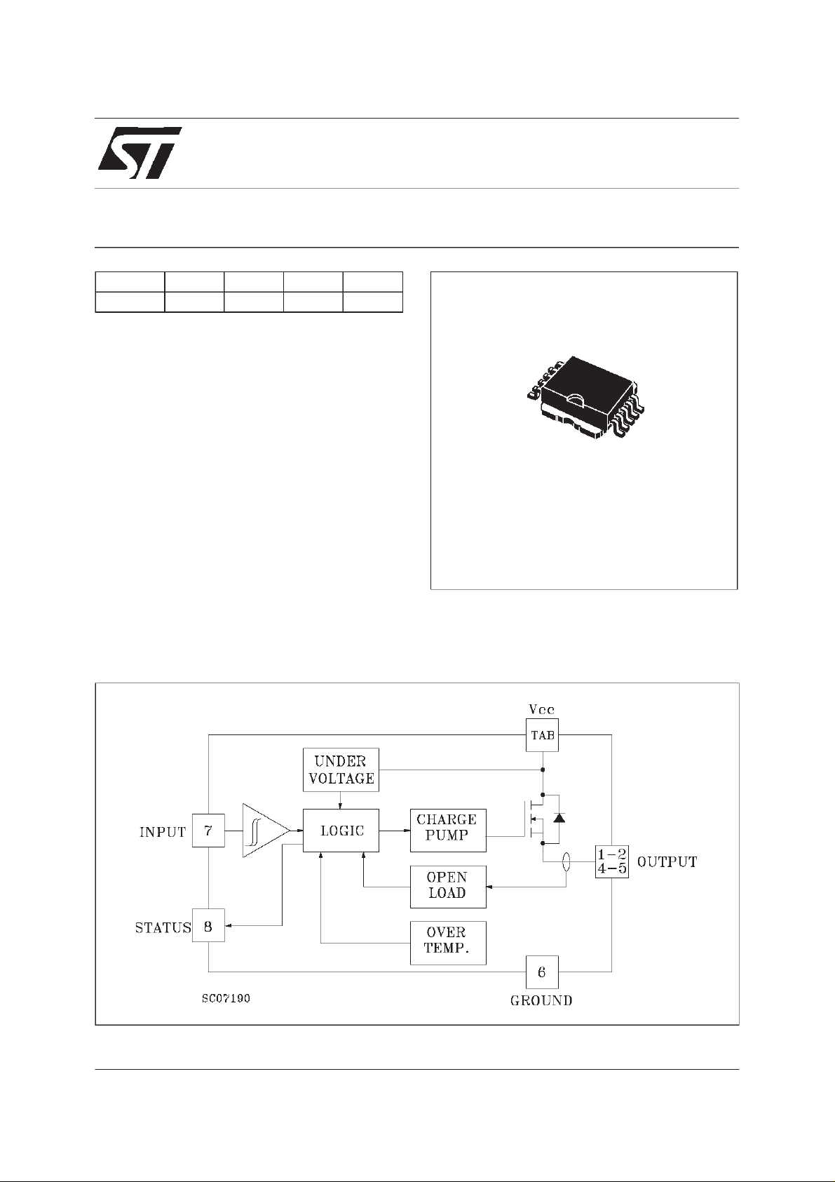
DESCRIPTION
The VN05NSP is a monolithic devices made
using STMicroelectronics VIPower Technology,
intended for driving resistive or inductive loads
with one side grounded.
Built-in thermal shut-down protects the chip from
over temperature and short circuit.
The input control is 5V logic level compatible.
The open drain diagnostic output indicates open
circuit(no load) andover temperaturestatus.
BLOCK DIAGRAM
10
1
PowerSO-10
June 1998
1/9
Page 2
VN05NSP
ABSOLUTEMAXIMUMRATING
Symbol Parameter Value Unit
V
(BR)DSS
I
OUT
I
I
-V
I
STAT
V
ESD
P
T
T
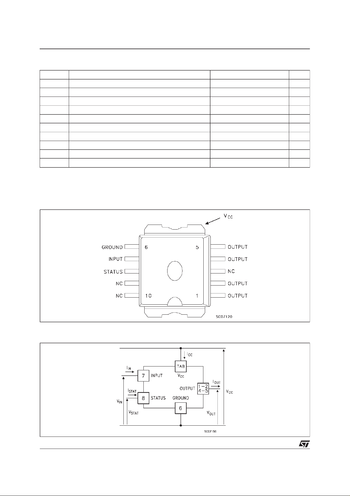
CONNECTIONDIAGRAMS
Drain-S o ur ce Breakdown V olt age 60 V
Out put Cu r rent (cont. ) 13 A
Revers e Out put Current -13 A
R
Input Current ±10 mA
IN
Reverse Supply V oltage -4 V
CC
St at us Cur rent ±10 mA
Elect r o st at ic Dischar ge (1.5 kΩ, 100 pF ) 2000 V
Power Dissipation at Tc≤ 25oC56W
tot
Junction O perat in g T em pe r at ure -40 t o 150
j
St orage Tem per atur e -55 t o 150
stg
o
C
o
C
CURRENT ANDVOLTAGE CONVENTIONS
2/9
Page 3
VN05NSP
THERMALDATA
R
thj-case
R
thj- amb
($) When mounted using minimum recommended pad size on FR-4 board
ELECTRICAL CHARACTERISTICS (VCC=13 V; -40 ≤ Tj≤ 125oC unless otherwisespecified)
POWER
Symbol Parameter Test Condition s Min. Typ. Max. Unit
V
R
I
SWITCHING
Symbol Parameter Test Condition s Min. Typ. Max. Unit
t
d(on)
t
d(off)
(di/dt)
(di/dt)
Ther mal Resis t ance Junc t io n-c ase Max
Therm al Res is tance J unction-ambient ($) Max
Supply Voltage 7 26 V
CC
On Stat e Resist a nce I
on
Supply Current Of f Stat e Tj≥ 25oC
S
=6A
OUT
=6A Tj=25oC
I
OUT
2.2
50
On State
Turn-on Delay Time Of
Out put Cu r rent
Rise TimeOf Output
t
r
Current
Turn-off Delay Time Of
Out put Cu r rent
Fall T ime Of Output
t
f
Current
Tur n-on Current S lope I
on
Tur n-of f C urrent Slope I
off
I
= 6 A Res istive Load
OUT
Input Rise Time < 0.1 µsT
I
= 6 A Res istive Load
OUT
Input Rise Time < 0.1 µsT
I
= 6 A Res istive Load
OUT
Input Rise Time < 0.1 µsT
I
= 6 A Res istive Load
OUT
Input Rise Time < 0.1 µsT
=6A
OUT
I
OUT=IOV
=6A
OUT
I
OUT=IOV
j
j
j
j
=25oC
=25oC
=25oC
=25oC
15 µs
30 µs
20 µs
10 µs
0.36
0.18
50
15
0.52A/µs
2
4
o
C/W
o
C/W
Ω
Ω
µA
mA
A/µs
A/µs
A/µs
LOGIC INPUT
Symbol Parameter Test Condition s Min. Typ. Max. Unit
V
Input Low Level
IL
0.8 V
Volt age
V
Input Hig h Lev el
IH
2(*)V
Volt age
V
I(hyst.)
Input Hysteresis
0.5 V
Volt age
I
V
Input Current VIN= 5 V 250 5 00 µA
IN
Input Cla m p Volt ag e IIN=10mA
ICL
=-10mA
I
IN
6
-0.7
PROTECTIONS AND DIAGNOSTICS
Symbol Parameter Test Condition s Min. Typ. Max. Unit
V
(•) St at us V oltage Output
STAT
Low
V
USD
Under Voltage Shut
Down
I
=1.6mA 0.4 V
STAT
6.5 V
V
V
3/9
Page 4

VN05NSP
ELECTRICAL CHARACTERISTICS (continued)
PROTECTION AND DIAGNOSTICS(continued)
Symbol Parameter Test Condition s Min. Typ. Max. Unit
V
(•) Stat us Clam p Volt age I
SCL
t
SC
I
OV
I
I
T
TSD
T
(*) The VIHis internally clamped at 6V about. Itis possible to connect this pin to an highervoltage via an external resistor calculated to not
exceed 10 mAat the input pin.
(•) Status determination >100 µs afterthe switching edge.
Swit ch-of f Tim e in
Short Circ u it Condition
at Start-Up
Over Current R
Aver age Current in
AV
Short Circuit
Open Load Cur rent
OL
Level
Ther mal Shut- d own
Tem perature
Reset Temperat u r e 125
R
=10mA
STAT
=-10mA
I
STAT
R
<10mΩ Tc=25oC1.55ms
LOAD
<10mΩ -40 Tc125oC60A
LOAD
R
<10mΩ Tc=85oC1.4A
LOAD
5180mA
140
6
-0.7
V
V
o
C
o
C
FUNCTIONAL DESCRIPTION
The device has a diagnostic output which
indicates open circuit (no load) and over
temperature conditions. The output signals are
processedby internal logic.
To protect the device against short circuit and
over-current condition, the thermal protection
turns the integrated Power MOS off ata minimum
junction temperature of 140
temperature returns to about 125
o
C. When the
o
C theswitch is
automaticallyturnedon again.
In short circuit conditions the protection reacts
with virtuallyno delay, the sensor being located in
the region of the die where the heat is generated.
PROTECTING THE DEVICE AGAINST
REVERSEBATTERY
The simplest way to protect the device against a
continuous reverse battery voltage (-26V) is to
insert a Schottky diode between pin 1 (GND) and
ground, as shown in the typical application circuit
(fig. 3).
The consequences of the voltage drop across
this diode are as follows:
- If the input is pulled to power GND, a negative
voltage of -V
thresholds and V
respectto power GND).
The undervoltageshutdown level is increased by
V
.
F
If there is no need for the control unit to handle
external analog signals referred to the power
GND, the best approach is to connect the
reference potential of the control unit to node [1]
(see application circuit infig. 4), which becomes
the common signal GND for the whole control
board.
In this way no shift of V
place and no negative voltage appears on the
INPUT pin; this solution allows the use of a
standard diode, with a breakdownvoltage able to
handle any ISO normalized negative pulses that
occours in the automotive environment.
is seen by the device. (VIL,V
F
are increased by VFwith
STAT
IH,VIL
and V
STAT
IH
takes
4/9
Page 5

TRUTH TABLE
INPUT OUTPUT DIAGNOSTIC
Normal Opera ti on L
H
Open Circ uit (No Load) H H L
Ov er- temperature H L L
Under-voltage X L H
L
H
Figure1: Waveforms
VN05NSP
H
H
Figure2: Over Current Test Circuit
5/9
Page 6

VN05NSP
Figure3: TypicalApplicationCircuit With A Schottky Diode ForReverse SupplyProtection
Figure4: TypicalApplicationCircuit With SeparateSignal Ground
6/9
Page 7

VN05NSP
R
DS(on)
R
DS(on)
vs Junction Temperature
Vs OutputCurrent
R
Vs SupplyVoltage
DS(on)
InputVoltage vs Junction Temperature
OutputCurrent Derating
OpenLoad vs Junction Temperature
7/9
Page 8

VN05NSP
PowerSO-10MECHANICAL DATA
DIM.
mm inch
MIN. TYP. MAX. MIN. TYP. MAX.
A 3.35 3.65 0.132 0.144
A1 0.00 0.10 0.000 0.004
B 0.40 0.60 0.016 0.024
c 0.35 0.55 0.013 0.022
D 9.40 9.60 0.370 0.378
D1 7.40 7.60 0.291 0.300
E 9.30 9.50 0.366 0.374
E1 7.20 7.40 0.283 0.291
E2 7.20 7.60 0.283 0.300
E3 6.10 6.35 0.240 0.250
E4 5.90 6.10 0.232 0.240
e 1.27 0.050
F 1.25 1.35 0.049 0.053
H 13.80 14.40 0.543 0.567
h 0.50 0.002
L 1.20 1.80 0.047 0.071
q 1.70 0.067
α 0
o
o
8
==
==
HE
h
A
F
A1
610
51
eB
M
0.25
D
==
D1
==
DETAIL”A”
E2
==
DETAIL”A”
Q
B
0.10 A
E1E3
==
SEATING
PLANE
A
C
α
B
E4
==
SEATING
PLANE
A1
L
==
0068039-C
8/9
Page 9

VN05NSP
Information furnished is believed tobe accurate and reliable.However, STMicroelectronics assumes no responsibility fortheconsequences
of use of such information nor for any infringement of patents or other rights of third parties which may result from its use. No license is
granted by implication orotherwise under any patent or patent rights of STMicroelectronics. Specification mentioned in this publication are
subject tochangewithoutnotice. This publication supersedes andreplaces all informationpreviously supplied.STMicroelectronics products
are not authorized for use as critical componentsin life support devices or systems withoutexpress written approval of STMicroelectronics.
Australia -Brazil - Canada- China - France- Germany- Italy- Japan - Korea- Malaysia -Malta- Mexico - Morocco - TheNetherlands -
Singapore- Spain- Sweden- Switzerland - Taiwan -Thailand - United Kingdom- U.S.A.
The ST logo isa trademarkof STMicroelectronics
1998 STMicroelectronics– Printed in Italy–AllRights Reserved
STMicroelectronicsGROUP OF COMPANIES
.
9/9
 Loading...