

Page 1

VN05N
HIGH SIDE SMART POWER SOLID STATE RELAY
TYPE V
VN05N 60 V 0.18 Ω 13 A 26 V
■ OUTPUT CURRENT (CONTINUOUS): 13A @
DSS
R
DS(on)
I
OUT
V
CC
Tc=25oC
■ 5V LOGIC LEVEL COMPATIBLE INPUT
■ THERMAL SHUT-DOWN
■ UNDER VOLTAGE SHUT-DOWN
■ OPEN DRAIN DIAGNOSTIC OUTPUT
■ VERY LOW STAND-BY POWER
DISSIPATION
DESCRIPTION
The VN05N is a monolithic device made using
SGS-THOMSON Vertical Intelligent Power
Technology, intended for driving resistive or
inductive loads with one side grounded.
Built-in thermal shut-down protects the chip from
over temperature and short circuit.
The input control is 5V logic level compatible.
The open drain diagnostic output indicates open
circuit (no load) and over temperature status.
BLOCK DIAGRAM
PENTAWATT
(vertical)
PENTAWATT
(horizontal)
PENTAWATT
(in-line)
ORDER CODES:
PENTAWATT vertical VN05N
PENTAWATT horizontal VN05N (011Y)
PENTAWATT in-line VN05N (012Y)
September 1994
1/11
Page 2
VN05N
ABSOLUTE MAXIMUM RATING
Symbol Parameter Value Uni t
V
(BR)DSS
I
OUT
I
I
-V
I
STAT
V
ESD
P
T
T
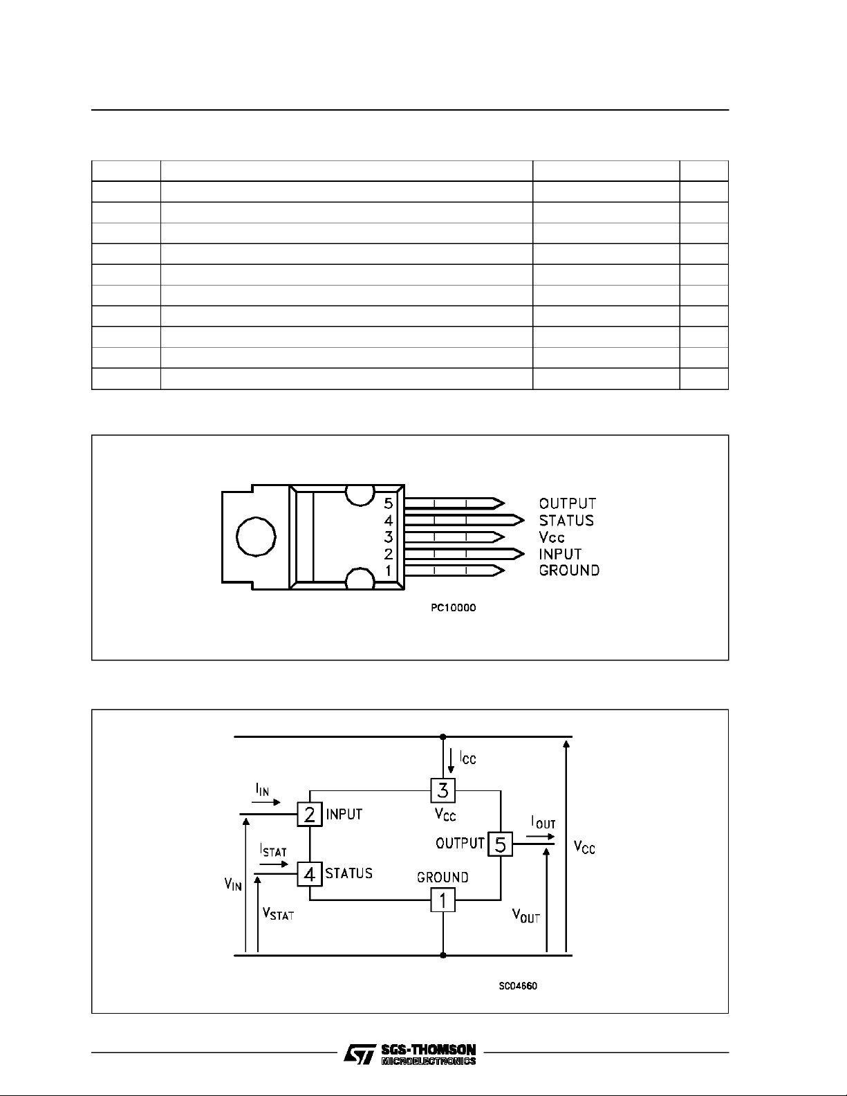
CONNECTION DIAGRAM
Drain - So urc e Br e ak down Vo ltage 60 V
Out put Current (cont. ) 13 A
Reverse O ut put Cu rr ent -13 A
R
Input Current ±10 mA
IN
Reverse Supply Voltage -4 V
CC
St at us Current ±10 mA
Electrost atic Dischar ge (1.5 kΩ, 100 pF) 2000 V
Powe r Dissipat ion at Tc≤ 25oC56W
tot
Junction Operati ng Tem per at ur e -40 t o 150
j
St or a ge Tem per ature -55 t o 150
stg
o
C
o
C
CURRENT AND VOLTAGE CONVENTIONS
2/11
Page 3

VN05N
THERMAL DATA
R
thj-case
R
thj-amb
ELECTRICAL CHARACTERISTICS (VCC= 13 V; -40 ≤ Tj≤ 125oC unless otherwise specified)
POWER
Symbol Parameter Test Co ndition s Min. Typ. Max. Unit
V
R
I
SWITCHING
Symbol Parameter Test Co ndition s Min. Typ. Max. Unit
t
d(on)
t
d(off)
(di/dt)
(di/dt)
Thermal Resistance Junction-c as e Max
Thermal Resist anc e Junc t ion-ambient Max
Supply Volta ge 7 26 V
CC
On State Res istance I
on
Supply Curr ent Of f Sta te Tj≥ 25oC
S
=6A
OUT
I
=6A Tj=25oC
OUT
2.2
60
On St ate
Turn-on Delay Time Of
Out put Current
Rise Time Of Ou t put
t
r
Current
Tur n - of f Delay T ime O f
Out put Current
t
Fall Time Of Output
f
Current
Turn-on Current S lope I
on
Turn-off Current Slope I
off
I
= 6 A Res istive Lo ad
OUT
Input Rise Time < 0.1 µsT
I
= 6 A Res istive Lo ad
OUT
=25oC
j
Input Rise Time < 0.1 µsTj=25oC
I
= 6 A Res istive Lo ad
OUT
Input Rise Time < 0.1 µsTj=25oC
I
= 6 A Res istive Lo ad
OUT
Input Rise Time < 0.1 µsTj=25oC
=6A
OUT
I
OUT=IOV
=6A
OUT
I
OUT=IOV
15 µs
30 µs
20 µs
10 µs
0.36
0.18
50
15
0.52A/µs
2
4
o
C/W
o
C/W
Ω
Ω
µA
mA
A/µs
A/µs
A/µs
LOGIC INPUT
Symbol Parameter Test Co ndition s Min. Typ. Max. Unit
V
Input LowLevel
IL
0.8 V
Volt age
V
Input High Level
IH
2(*)V
Volt age
V
I(hyst.)
Input Hys teresis
0.5 V
Volt age
I
V
Input Current VIN= 5 V 250 500 µA
IN
Input Clamp Voltage IIN=10mA
ICL
IIN=-10mA
6
-0.7
PROTECTIONS AND DIAGNOSTICS
Symbol Parameter Test Co ndition s Min. Typ. Max. Unit
(•) Status Voltage Output
V
STAT
Low
V
USD
Under Voltage S hut
Down
I
=1.6mA 0.4 V
STAT
6.5 V
V
V
3/11
Page 4

VN05N
ELECTRICAL CHARACTERISTICS (continued)
PROTECTION AND DIAGNOSTICS (continued)
Symbol Parameter Test Co ndition s Min. Typ. Max. Unit
(•) Status Clamp Voltage I
V
SCL
t
SC
I
OV
I
AV
I
OL
T
TSD
T
(*) The VIHis internally cl am ped at 6V about . It is possible to connect this pin to an higher vol t age v ia an external resistor
cal culated to not exceed 10 mA at the input pin.
(•) Status deter m ination > 100 µ s after the switching edge.
Switc h-off Time in
Short Circuit Condition
at Start-Up
Ove r Current R
Aver age Current in
Short Circuit
Open Load Cu r rent
Level
Thermal Shut-down
Tem perature
Reset Temper ature 125
R
=10mA
STAT
I
=-10mA
STAT
R
<10mΩ Tc=25oC 1.55ms
LOAD
<10mΩ -40 ≤ Tc≤ 125oC60A
LOAD
R
<10mΩ Tc=85oC1.4A
LOAD
5 180 mA
140
6
-0.7
V
V
o
C
o
C
FUNCTIONAL DESCRIPTION
The device has a diagnostic output which
indicates open circuit (no load) and over
temperature conditions. The output signals are
processed by internal logic.
To protect the device against short circuit and
over-current condition, the thermal protection
turns the integrated Power MOS off at a minimum
junction temperature of 140oC. When the
temperature returns to about 125oC the switch is
automatically turned on again.
In short circuit conditions the protection reacts
with virtually no delay, the sensor being located in
the region of the die where the heat is generated.
PROTECTING THE DEVICE AGAINST REVERSE BATTERY
The simplest way to protect the device against a
continuous reverse battery voltage (-26V) is to
insert a Schottky diode between pin 1 (GND) and
ground, as shown in the typical application circuit
(fig. 3).
The consequences of the voltage drop across
this diode are as follows:
– If the input is pulled to power GND, a negative
voltage of -VFis seen by the device. (VIL,V
thresholds and V
are increased by VFwith
STAT
respect to power GND).
IH
– The undervoltage shutdown level is increased
by VF.
If there is no need for the control unit to handle
external analog signals referred to the power
GND, the best approach is to connect the
reference potential of the control unit to node [1]
(see application circuit in fig. 4), which becomes
the common signal GND for the whole control
board.
In this way no shift of VIH,VILand V
place and no negative voltage appears on the
INPUT pin; this solution allows the use of a
standard diode, with a breakdown voltage able to
handle any ISO normalized negative pulses that
occours in the automotive environment.
STAT
takes
4/11
Page 5

TRUTH TABLE
INPUT OUTPUT DIAG NO ST IC
Normal O peration L
H
Open Circuit (No Load) H H L
Ove r -temperature H L L
Under-v oltage X L H
L
H
Figure 1: Waveforms
VN05N
H
H
Figure 2: Over Current Test Circuit
5/11
Page 6

VN05N
Figure 3: Typical Application Circuit With A Schottky Diode For Reverse Supply Protection
Figure 4: Typical Application Circuit With Separate Signal Ground
6/11
Page 7

VN05N
R
DS(on)
R
DS(on)
vs Junction Temperature R
vs Supply Voltage
DS(on)
vs Output Current Input voltages vs Junction Temperature
Output Current Derating Open Load vs Junction Temperature
7/11
Page 8

VN05N
Pentawatt (vertical) MECHANICAL DATA
DIM.
MIN. TYP. MAX. MIN. TYP. MAX.
mm inch
A 4.8 0.189
C 1.37 0.054
D 2.4 2.8 0.094 0.110
D1 1.2 1.35 0.047 0.053
E 0.35 0.55 0.014 0.022
F 0.8 1.05 0.031 0.041
F1 1 1.4 0.039 0.055
G 3.2 3.4 3.6 0.126 0.134 0.142
G1 6.6 6.8 7 0.260 0.268 0.276
H2 10.4 0.409
H3 10.05 10.4 0.396 0.409
L 17.85 0.703
L1 15.75 0.620
L2 21.4 0.843
L3 22.5 0.886
L5 2.6 3 0.102 0.118
L6 15.1 15.8 0.594 0.622
L7 6 6.6 0.236 0.260
M 4.5 0.177
M1 4 0.157
Dia 3.65 3.85 0.144 0.152
A
H3
L
L1
C
D1
Dia.
L7
L6
L2
L3L5
D
F1
H2
E
MM1
G1
G
F
P010E
8/11
Page 9

Pentawatt (horizontal) MECHANICAL DATA
VN05N
DIM.
A 4.8 0.189
C 1.37 0.054
D 2.4 2.8 0.094 0.110
D1 1.2 1.35 0.047 0.053
E 0.35 0.55 0.014 0.022
F 0.8 1.05 0.031 0.041
F1 1 1.4 0.039 0.055
G 3.2 3.4 3.6 0.126 0.134 0.142
G1 6.6 6.8 7 0.260 0.268 0.276
H2 10.4 0.409
H3 10.05 10.4 0.396 0.409
L 14.2 15 0.559 0.590
L1 5.7 6.2 0244
L2 14.6 15.2 0.598
L3 3.5 4.1 0.137 0.161
L5 2.6 3 0.102 0.118
L6 15.1 15.8 0.594 0.622
L7 6 6.6 0.236 0.260
Dia 3.65 3.85 0.144 0.152
MIN. TYP. MAX. MIN. TYP. MAX.
mm inch
P010F
9/11
Page 10

VN05N
Pentawatt (In- Line) MECHANICAL DATA
DIM.
MIN. TYP. MAX. MIN. TYP. MAX.
A 4.8 0.189
C 1.37 0.054
D 2.4 2.8 0.094 0.110
D1 1.2 1.35 0.047 0.053
E 0.35 0.55 0.014 0.022
F 0.8 1.05 0.031 0.041
F1 1 1.4 0.039 0.055
G 3.2 3.4 3.6 0.126 0.134 0.142
G1 6.6 6.8 7 0.260 0.268 0.276
H2 10.4 0.409
H3 10.05 10.4 0.396 0.409
L2 23.05 23.4 23.8 0.907 0.921 0.937
L3 25.3 25.65 26.1 0.996 1.010 1.028
L5 2.6 3 0.102 0.118
L6 15.1 15.8 0.594 0.622
L7 6 6.6 0.236 0.260
Dia 3.65 3.85 0.144 0.152
mm inch
10/11
P010D
Page 11

VN05N
Information furnished is believed to be accurate and reliable. However, SGS-THOMSON Microelectronics assumes no responsability for the
consequences of use of such information nor for any infringement of patents or other rights of third parties which mayresults from its use. No
license is grantedby implication or otherwise under anypatent or patent rights of SGS-THOMSON Microelectronics.Specificationsmentioned
in this publicationare subject to change without notice. This publication supersedes and replaces all information previously supplied.
SGS-THOMSON Microelectronicsproductsarenot authorizedforuse as criticalcomponents inlife supportdevices or systemswithout express
written approval of SGS-THOMSON Microelectonics.
1994SGS-THOMSON Microelectronics- All RightsReserved
Australia - Brazil - France - Germany - Hong Kong - Italy - Japan - Korea - Malaysia - Malta - Morocco - The Netherlands -
Singapore - Spain - Sweden - Switzerland -Taiwan - Thailand - United Kingdom - U.S.A
SGS-THOMSON Microelectronics GROUP OF COMPANIES
11/11
 Loading...