

Page 1
VN03SP
HIGH SIDE SMART POWER SOLID STATE RELAY
TYPE V
DSS
R
DS(on)
I
n(*)
V
CC
VN03SP 60 V 0.5 Ω 0.7 A 26 V
■ MAXIMUMCONTINUOUS OUTPUT
CURRENT(#):9 A @ T
■ 5 V LOGIC LEVEL COMPATIBLEINPUT
■ THERMALSHUT-DOWN
■ UNDERVOLTAGE PROTECTION
■ OPENDRAIN DIAGNOSTIC OUTPUT
■ INDUCTIVELOAD FAST
=85oC
c
DEMAGNETIZATION
■ VERY LOW STAND-BY POWER
DISSIPATION
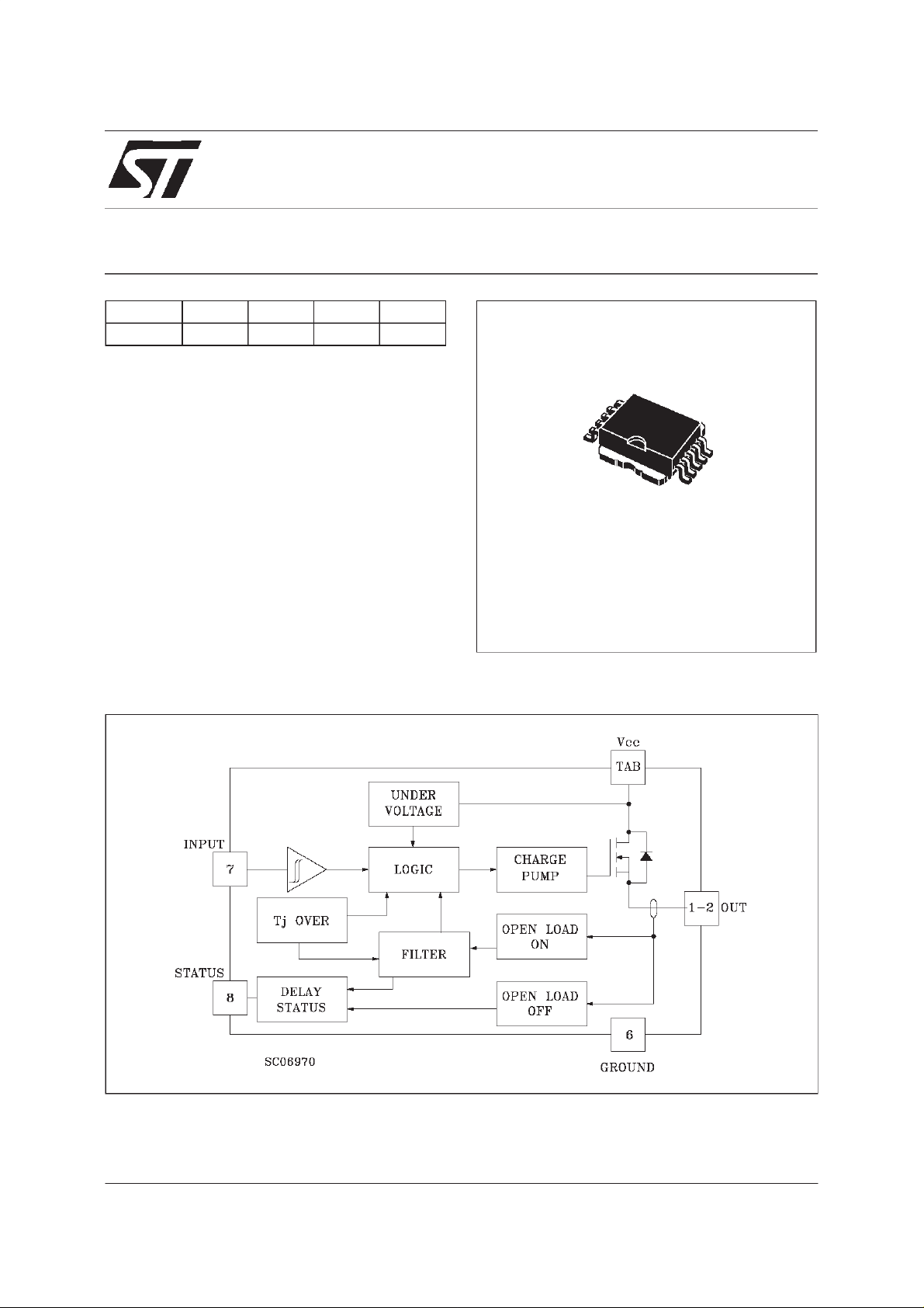
DESCRIPTION
The VN03SP is a monolithic device made using
STMicroelectronics VIPower Technology,
intended for driving resistive or inductive loads
with one side grounded.
Built-in thermal shut-down protects the chip from
over temperatureand short circuit.
The open drain diagnostic output indicates: open
load in off state, and in on state, output shorted to
10
1
PowerSO-10
V
and overtemperature. Fast demagnetization
CC
of inductive loads is archivied by negative (-18V)
load voltageat turn-off.
(*) In = Nominal current according to ISO definition for high side automotive switch (see note 1)
(#) The maximum continuous output current is the the current at T
protection.
=85oC for a battery voltage of 13V which doesnot activate self
c
July 1998
1/9
Page 2
VN03SP
ABSOLUTEMAXIMUMRATING
Symb o l Para met er Val u e Uni t
V
(BR)DSS
I
OUT
I
I
-V
I
STAT
V
ESD
P
T
T
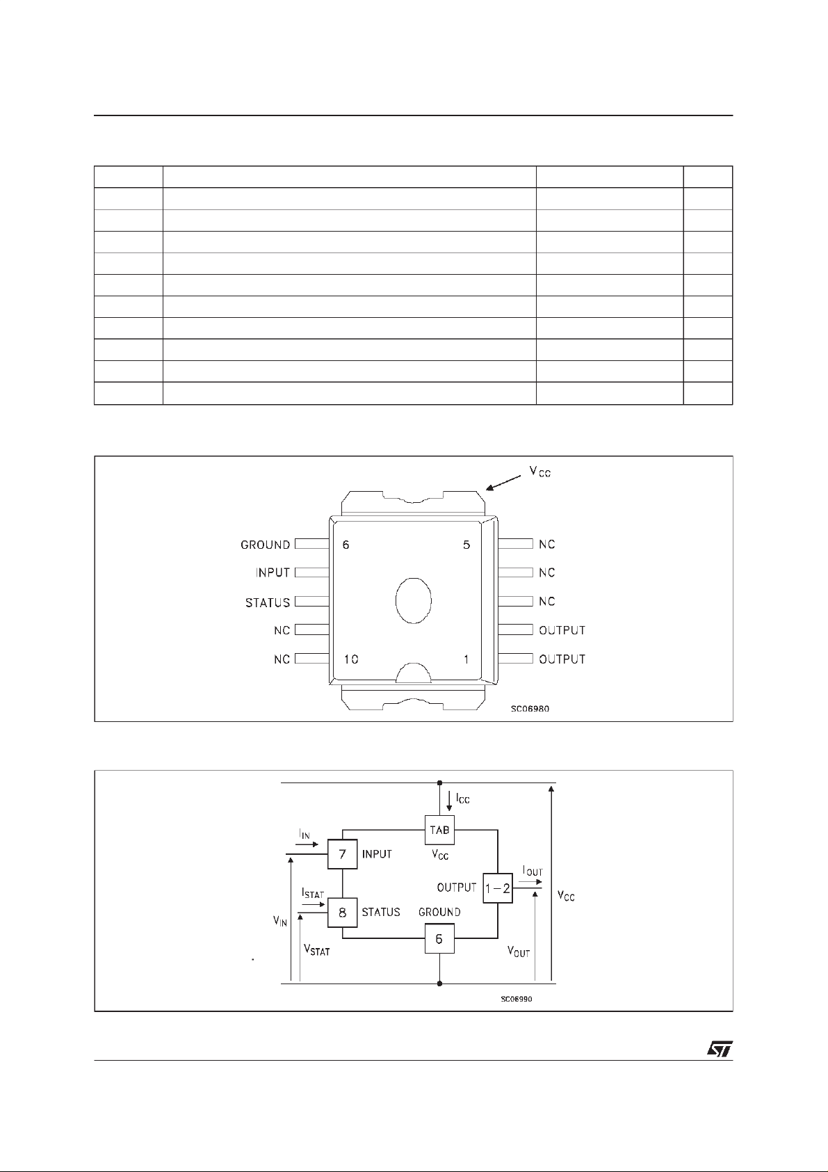
CONNECTIONDIAGRAMS
Drain-S o ur ce Breakdown V olt ag e 60 V
Out put Current (con t . ) at Tc=85oC4A
Revers e Out put Curr ent at Tc=85oC-4A
R
Input Current ±10 mA
IN
Reverse Supply Voltage -4 V
CC
St at us Cu rr ent ±10 mA
Elect r o st at ic D ischarge ( 1. 5 kΩ, 100 pF) 2000 V
Power Dissipation at Tc=85oC14W
tot
Junction Oper at in g Temperat ure -40 t o 150
j
St orage Tem per atur e -55 t o 150
stg
o
C
o
C
CURRENT ANDVOLTAGECONVENTIONS
2/9
Page 3
VN03SP
THERMALDATA
R
thj-case
R
thj-amb
($) When mounted using minimum recommended pad size on FR-4 board
ELECTRICAL CHARACTERISTICS (VCC=13 V; -40 ≤ Tj≤ 125oC unless otherwisespecified)
POWER
Symbol Parameter Test C ondition s Min. Typ. Max. Unit
V
In(*) Nominal Current T
R
I
V
DS(MAX)
SWITCHING
Symbol Parameter Test C ondition s Min. Typ. Max. Unit
t
d(on)
t
r
t
d(off)
t
f
(di/dt)
(di/dt)
V
demag
Ther mal Resis t ance Junct ion-cas e Max
Ther mal Resis t ance Junct ion-ambient ($) Max
Supply Voltag e 5.5 13 26 V
CC
=85oCV
c
On State Resi st a nc e I
on
Supply Current Of f Stat e Tj≥ 25oC
S
=0.7A
OUT
I
=0.7A Tj=25oC
OUT
≤ 0. 5 (note 1) 0.7 A
DS(on)
4.5
50
On State
Maximum Voltage Drop I
(^) Tur n-on Delay Tim e Of
Out put Current
(^) Rise T ime O f O utput
Current
(^) Tur n-of f Delay Time Of
Out put Current
(^) Fall Time Of Output
Current
Tur n-on Current S lope I
on
Tur n-of f C urr ent Slope I
off
Induc t i ve L oad Clamp
=4A Tc=85oC3.6V
OUT
I
= 0.7 A Resist iv e Load
OUT
15 µs
Input Rise T im e < 0. 1 µs
I
= 0.7 A Resist iv e Load
OUT
10 µs
Input Rise T im e < 0. 1 µs
I
= 0.7 A Resist iv e Load
OUT
15 µs
Input Rise T im e < 0. 1 µs
I
= 0.7 A Resist iv e Load
OUT
4 µs
Input Rise T im e < 0. 1 µs
=0.7A
OUT
I
OUT=IOV
=0.7A
OUT
I
OUT=IOV
I
=0.7A L=1mH -24 -18 -14 V
OUT
0.05 0.51A/µs
0.14 3
Volt age
1
0.5
50
15
3
o
C/W
o
C/W
Ω
Ω
µA
mA
A/µs
A/µs
A/µs
LOGIC INPUT
Symbol Parameter Test C ondition s Min. Typ. Max. Unit
V
V
V
I(hyst.)
I
V
Input Low Lev el
IL
Volt age
Input High Level
IH
Volt age
Input Hysteresis
Volt age
Input Current VIN=5V
IN
Input Clamp Voltage IIN=10mA
ICL
=2V
V
IN
=0.8V 25
V
IN
=-10mA
I
IN
0.8 V
2(•)V
0.5 V
250 5 00
250
5.5 6
-0.7 -0.3
µA
µA
µA
V
V
3/9
Page 4

VN03SP
ELECTRICAL CHARACTERISTICS(continued)
PROTECTION AND DIAGNOSTICS
Symbol Parameter Test C ondition s Min. Typ. Max. Unit
V
STAT
V
USD
V
SCL
I
OV
I
I
T
TSD
T
V
t
1(on)
t
1(off)
t
2(off)
t
povl
t
pol
(^) See Switchig Time Waveforms
() The V
exceed 10 mA at the input pin.
note 1:The Nominal Current is the current at T
note 2:I
note 3:t
: minimum load recovery time which desactivates the statusoutput
t
1(off)
t
: minimum on time after thermal shut down which desactivates status output
2(off)
t
povltpol
St at us V olt age Output
I
=1.6mA 0.4 V
STAT
Low
Under V ol ta ge S hut
5V
Down
St at us Cl amp V olt age I
Over Current R
Aver age Current in
AV
=10mA
STAT
=-10mA
I
STAT
<10mΩ -40 Tc125oC28A
LOAD
R
<10mΩ Tc=85oC0.9A
LOAD
6
-0.7
Short Circuit
Open Loa d Cur rent
OL
53570mA
Level
Ther mal Shut-d ow n
140
Tem perature
Reset T emperatu re 125
R
Open Loa d Vo lt age
OL
Of f - State (no te 2) 2.5 3.75 5 V
Level
Open Loa d Fil t er ing
(note 3) 1 5 10 ms
Time
Open Loa d Fil t er ing
(note 3) 1 5 10 ms
Time
Open Loa d Fil t er ing
(note 3) 1 5 10 ms
Time
St at us De lay (note 3) 5 10 µs
St at us De lay (note 3) 50 700 µs
is internally clamped at 6V about. It is possible to connect this pinto an higher voltagevia an external resistor calculated to not
IH
=85oC for battery voltage of 13V which produces a voltage drop of 0.5 V
=(VCC-VOL)/ROL(see figure)
OL(off)
: minimum open load duration which acctivates the status output
1(on)
: ISO definition (see figure)
c
V
V
o
C
o
C
Note2 RelevantFigure Note 3 Relevant Figure
4/9
Page 5

VN03SP
SwitchingTime Waveforms
FUNCTIONAL DESCRIPTION
The device has a diagnostic output which
indicates open load conditions in off state as well
as in on state, output shorted to V
CC
and
overtemperature. The truth table shows input,
diagnostic and output voltage level in normal
operation and in fault conditions. The output
signals are processed by internal logic. The
open load diagnostic output has a 5 ms filtering.
The filter gives a continuous signal for the fault
condition after an initialdelay of about 5 ms. This
means that a disconnection during normal
operation, with a duration of less than 5 ms does
not affect the status output. Equally, any
re-connection of less than 5 ms during a
disconnection duration does not affect the status
output. No delay occur for the status to go low in
case of overtemperature conditions. From the
falling edge of the input signal the status output
initially low in fault condition (over temperature or
open load) will go back with a delay (t
of overtemperature condition and a delay (t
)in case
povl
pol
)in
case of open load. These feature fully comply
with International Standard Office (I.S.O.)
requirement for automotiveHighSide Driver.
To protect the device against short circuit and
over current conditions, the thermal protection
turns the integrated Power MOS off at a
minimum junction temperature of 140
When the temperature returns to 125
o
C the
o
C.
switch is automatically turned on again.In short
circuit the protection reacts with virtually no
delay, the sensor being located in the region of
the die where the heat is generated. Driving
inductive loads, an internal function of the
device ensures the fast demagnetizationwith a
typicalvoltage (V
demag
) of -18V.
This function allows to greatly reduce the power
dissipationaccording to the formula:
P
dem
= 0.5 • L
load
• (I
load
)2• [(VCC+V
demag
)/V
demag
•f
where f = switchingfrequency and
V
=demagnetizationvoltage
demag
Based on this formula it is possible to know
the value of inductance and/or current to avoid
a thermal shut-down. The maximum inductance
which causes the chip temperature to reach the
shut down temperature in a specific thermal
environment, is infact a function of the load
currentfor a fixed V
CC,Vdemag
and f.
PROTECTING THE DEVICE AGAIST LOAD
DUMP - TEST PULSE 5
The device is able to withstand the test pulse
No. 5 at level II (V
= 46.5V) according to the
s
ISO T/R 7637/1 without any external
component. This means that all functions of the
device are performed as designed after
exposure to disturbance at level II. The VN06SP
is able to withstand the test pulse No.5 at level
III adding an external resistor of 150 ohm
between GND pin and ground plus a filter
capacitor of 1000 µF between V
ground(if R
LOAD
≤ 20 Ω).
CC
pin and
PROTECTING THE DEVICE AGAINST
REVERSE BATTERY
The simplest way to protect the device against a
continuous reverse battery voltage (-26V) is to
insert a Schottky diode between GND pin and
ground, as shown in the typical application circuit
(fig.3).
The consequences of the voltage drop across
this diode are as follows:
If the input is pulled to power GND, a negative
voltage of -V
is seen by the device. (Vil, Vih
f
thresholds and Vstat are increased by Vf with
respect to power GND).
The undervoltageshutdown level is increa- sed
by Vf.
If there is no need for the control unit to handle
external analog signals referred to the power
GND, the best approach is to connect the
reference potential of the control unit to node [6]
(see application circuit in fig. 4), which becomes
the common signal GND for the whole control
board avoiding shift of V
,Viland V
ih
stat
. This
solutionallows theuse of a standard diode.
]
5/9
Page 6

VN03SP
TRUTH TABLE
INPUT OUTPUT DIAGNOSTIC
Normal Opera ti on L
H
Open Ci rc uit (No Load) H H L
Ov er- tempera tu re H L L
Under-voltage X L H
ShortloadtoV
CC
LHL
Figure1: Waveforms
L
H
H
H
Figure2: Over Current Test Circuit
6/9
Page 7

Figure3: TypicalApplicationCircuitWith A SchottkyDiode For Reverse SupplyProtection
VN03SP
Figure4: TypicalApplicationCircuitWith Separate Signal Ground
7/9
Page 8

VN03SP
PowerSO-10MECHANICAL DATA
DIM.
mm inch
MIN. TYP. MAX. MIN. TYP. MAX.
A 3.35 3.65 0.132 0.144
A1 0.00 0.10 0.000 0.004
B 0.40 0.60 0.016 0.024
c 0.35 0.55 0.013 0.022
D 9.40 9.60 0.370 0.378
D1 7.40 7.60 0.291 0.300
E 9.30 9.50 0.366 0.374
E1 7.20 7.40 0.283 0.291
E2 7.20 7.60 0.283 0.300
E3 6.10 6.35 0.240 0.250
E4 5.90 6.10 0.232 0.240
e 1.27 0.050
F 1.25 1.35 0.049 0.053
H 13.80 14.40 0.543 0.567
h 0.50 0.002
L 1.20 1.80 0.047 0.071
q 1.70 0.067
α 0
o
o
8
==
==
HE
h
A
F
A1
610
51
eB
M
0.25
D
==
D1
==
DETAIL”A”
E2
==
DETAIL”A”
Q
B
0.10 A
E1E3
==
SEATING
PLANE
A
C
α
B
E4
==
SEATING
PLANE
A1
L
==
0068039-C
8/9
Page 9

VN03SP
Information furnished isbelieved tobe accurate and reliable. However, STMicroelectronics assumes no responsibility forthe consequences
of use of such information nor for any infringement of patents or other rights of third parties which may result from its use. No license is
granted by implication or otherwise under any patent or patent rights ofSTMicroelectronics. Specification mentioned in this publication are
subject tochange without notice. This publication supersedes and replaces allinformation previously supplied.STMicroelectronics products
are not authorized foruse as critical componentsin life support devices or systems withoutexpress written approvalof STMicroelectronics.
Australia - Brazil - Canada- China - France- Germany - Italy- Japan - Korea- Malaysia - Malta - Mexico - Morocco- The Netherlands-
Singapore- Spain - Sweden- Switzerland- Taiwan -Thailand - United Kingdom- U.S.A.
The ST logo isa trademarkof STMicroelectronics
1998 STMicroelectronics– Printed in Italy – All Rights Reserved
STMicroelectronicsGROUP OFCOMPANIES
.
9/9
 Loading...