

Page 1
HIGH SIDE SMART POWER SOLID STATE RELAY
TYPE V
VN02NSP 60 V 0.4 Ω 6 A 26 V
VN02NPT 60 V 0.4 Ω 6 A 26 V
■ OUTPUT CURRENT (CONTINUOUS):
6A @ T
■ 5V LOGIC LEVEL COMPATIBLE INPUT
■ THERMAL SHUT-DOWN
■ UNDER VOLTAGE SHUT- DO WN
■ OPEN DRAIN DIAGNOSTIC OUTPUT
■ VERY LOW STAND-BY POWER
=25oC
c
DSS
DISSIPATION
R
DS(on
)I
OUT
V
VN02NSP
VN02NPT
PRELIMINARY DATA
CC
10
1
DESCRIP TION
The VN02NSP/VN02NPT are monolithic devices
made using SGS-THOMSON Vertical Intelligent
Power Technology, intended for driving resistive
or inductive loads with one side grounded.
Built-in thermal shut-down protects the chip from
over temperature and short circ uit.
The input control is 5V logic level compatible.
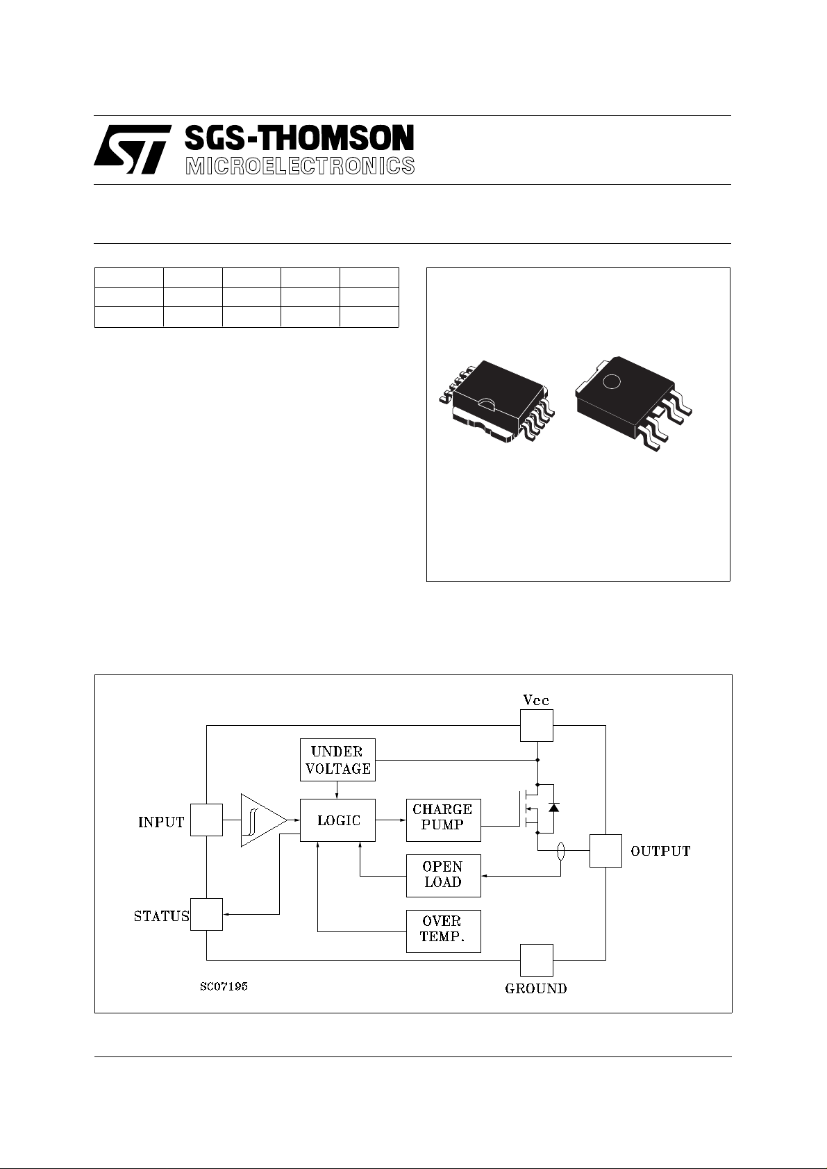
BLOCK DIAG RAM
PowerSO-10TM PPAK
The open drain diagnostic output indicates open
circuit (no load) and over temperature status.
September 1997
1/10
Page 2

VN02NSP/VN02NPT
ABSOLUTE MAXIMUM RATING
Symbol Parameter Value Unit
PowerSO-10 PPAK
V
(BR)DSS
I
OUT
I
I
-V
I
STAT
V
ESD
P
T
T
CONNECTION DIAGRAMS
Drain-Source Breakdown Voltage 60 V
Output Current (cont.) 6 A
Reverse Output Current -6 A
R
Input Current ±10 mA
IN
Reverse Supply Voltage -4 V
CC
Status Current ±10 mA
Electrostatic Discharge (1.5 kΩ, 100 pF)
Power Dissipation at Tc ≤ 25 oC
tot
Junction Operating Temperature -40 to 150
j
Storage Temperature -55 to 150
stg
2000 V
58 46 W
o
C
o
C
CURRENT AND VOLTAGE CONVENTI ONS
2/10
Page 3

VN02NSP/VN02NPT
THERMAL DATA
PowerSO-10 PPAK
R
thj-case
R
thj-amb
($) When mounted using minimum recommended pad size on FR-4 board
ELECTRICAL CHARACTERISTICS (VCC = 13 V; -40 ≤ Tj ≤ 125 oC unless otherwise specified)
POWER
Symbol Parameter Test Conditions Min. Typ. Max. Unit
V
R
I
SWITCHING
Symbol Parameter Test Conditions Min. Typ. Max. Unit
t
d(on)
t
d(off)
(di/dt)
(di/dt)
Thermal Resistance Junction-case Max
Thermal Resistance Junction-ambient ($) Max
Supply Voltage 7 26 V
CC
On State Resistance I
on
Supply Current
S
= 3 A
OUT
I
= 3 A Tj = 25 oC
OUT
Off State T
≥ 25 oC
j
2.14
62.5
On State
Turn-on Delay Time Of
Output Current
t
Rise Time Of Output
r
Current
Turn-off Delay Time Of
Output Current
t
Fall Time Of Output
f
Current
Turn-on Current Slope I
on
Turn-off Current Slope I
off
I
= 3 A Resistive Load
OUT
Input Rise Time < 0.1 µs T
I
= 3 A Resistive Load
OUT
Input Rise Time < 0.1 µs T
I
= 3 A Resistive Load
OUT
Input Rise Time < 0.1 µs T
I
= 3 A Resistive Load
OUT
Input Rise Time < 0.1 µs T
= 3 A
OUT
I
= IOV
OUT
= 3 A
OUT
I
= I
OUT
OV
= 25 oC
j
= 25 oC
j
= 25 oC
j
= 25 oC
j
10 µs
15 µs
15 µs
6 µs
3.33
100
0.8
0.4
50
15
0.52A/µs
2
4
o
C/W
o
C/W
Ω
Ω
µA
mA
A/µs
A/µs
A/µs
LOGIC INP UT
Symbol Parameter Test Conditions Min. Typ. Max. Unit
V
V
V
I(hyst.)
I
V
Input Low Level
IL
Voltage
Input High Level
IH
2(*)V
Voltage
Input Hysteresis
0.5 V
Voltage
Input Current VIN = 5 V 250 500 µA
IN
Input Clamp Voltage IIN = 10 mA
ICL
I
= -10 mA
IN
6
-0.7
0.8 V
V
V
3/10
Page 4

VN02NSP/VN02NPT
ELECTRICAL CHARACTERISTICS (continued)
PROTECT IO N AND DIAG NO S TIC S
Symbol Parameter Test Conditions Min. Typ. Max. Unit
V
(•) Status Voltage Output
STAT
V
USD
V
SCL
t
SC
I
OV
I
AV
I
OL
T
TSD
T
(*) The VIH is internally clamped at 6V about. It is possible to connect this pin to an higher voltage via an external resistor calculated to not
exceed 10 mA at the input pin. @NOTE = () Status determination > 100 µs after the switching edge.
Low
Under Voltage Shut
Down
() Status Clamp Voltage I
Switch-off Time in
Short Circuit Condition
at Start-Up
Over Current
Average Current in
Short Circuit
Open Load Current
Level
Thermal Shut-down
Temperature
Reset Temperature 125
R
I
= 1.6 mA 0.4 V
STAT
6.5 V
= 10 mA
STAT
I
= -10 mA
STAT
R
< 10 mΩ Tc = 25 oC
LOAD
R
< 10 mΩ -40 Tc 125 oC
LOAD
R
< 10 mΩ Tc = 85 oC
LOAD
570mA
140
6
-0.7
1.5 5 ms
0.9 A
28 A
o
o
V
V
C
C
FUNCTIONAL DES CRI PT ION
The device has a diagnostic output which
indicates open circuit (no load) and over
temperature conditions. The output signals are
processed by internal logic.
To protect the device against short circuit and
over-current condition, the thermal protection
turns the integrated Power MO S off at a minimum
junction temperature of 140
temperature returns to about 125
o
C. When the
o
C the switch is
automatically turned on again.
In short circuit conditions the protection reacts
with virtually no delay, the sensor being located in
the region of the die where the heat is generated.
PROTECTING THE DEVICE AGAINST
REVERSE BATTERY
The simplest way to protect the device against a
continuous reverse battery voltage (-26V) is to
insert a Schottky diode between pin 1 (GND) and
ground, as shown in the typical application circuit
(fig. 3).
The consequences of the voltage drop across
this diode are as follows:
- If the input is pulled to power GND, a negative
voltage of -V
thresholds and V
respect to power GND).
The undervoltage shutdown level is increased by
V
.
F
If there is no need for the control unit to handle
external analog signals referred to the power
GND, the best approach is to connect the
reference potential of the control unit to node [1 ]
(see application circuit infig. 4), which becomes
the common signal GND for the whole control
board.
In this way no shift of V
place and no negative voltage appears on the
INPUT pin; this solution allows the use of a
standard diode, with a breakdown voltage able to
handle any ISO normalized negative pulses that
occours in the automotive environment.
is seen by the device. (VIL, V
F
are increased by VF with
STAT
, VIL and V
IH
STAT
takes
IH
4/10
Page 5

VN02NSP/VN02NPT
TRUTH TABLE
INPUT OUTPUT DIAGNOSTIC
Normal Operation L
H
Open Circuit (No Load) H H L
Over-temperature H L L
Under-voltage X L H
Figure 1: Waveforms
L
H
H
H
Figure 2: Over Current Test Circuit
5/10
Page 6

VN02NSP/VN02NPT
Figure 3: Typical Application Circuit With A Schott ky Diode For Reverse Supply Prot ection
Figure 4: Typical Application Circuit With Separ ate Signal Gr ound
6/10
Page 7

VN02NSP/VN02NPT
R
DS(on)
R
DS(on)
vs Junction Temperature
Vs Output Current
R
Vs Supply Voltage
DS(on)
Input Voltage vs Junction Temperat ure
Output Current Derating
Open Load vs Junction Temperature
7/10
Page 8

VN02NSP/VN02NPT
PowerSO-10 MECHANICAL DATA
DIM.
mm inch
MIN. TYP. MAX. MIN. TYP. MAX.
A 3.35 3.65 0.132 0.144
A1 0.00 0.10 0.000 0.004
B 0.40 0.60 0.016 0.024
c 0.35 0.55 0.013 0.022
D 9.40 9.60 0.370 0.378
D1 7.40 7.60 0.291 0.300
E 9.30 9.50 0.366 0.374
E1 7.20 7.40 0.283 0.291
E2 7.20 7.60 0.283 0.300
E3 6.10 6.35 0.240 0.250
E4 5.90 6.10 0.232 0.240
e1.27 0.050
F 1.25 1.35 0.049 0.053
H 13.80 14.40 0.543 0.567
h0.50 0.002
L 1.20 1.80 0.047 0.071
q1.70 0.067
α0
o
o
8
= =
HE
h
A
F
A1
= =
0.25
e
M
D
= =
D1
= =
B
610
51
E2
= =
DETAIL "A"
DETAIL "A"
Q
B
0.10
E1E3
= =
SEATING
PLANE
A
C
α
B
A
E4
= =
SEATING
PLANE
A1
L
= =
0068039-C
8/10
Page 9

PPAK MECHANICAL DATA
VN02NSP/VN02NPT
DIM.
mm inch
MIN. TYP. MAX. MIN. TYP. MAX.
A 2.2 2.4 0.086 0.094
A1 0.9 1.1 0.035 0.043
A2 0.03 0.23 0.001 0.009
B0.5 0.019
B2 5.2 5.4 0.204 0.212
C 0.45 0.53 0.017 0.021
C2 0.5 0.019
D 6 6.2 0.236 0.244
E 6.4 6.6 0.252 0.260
G5.08 0.200
G1 2.54 0.100
H 9.35 10.1 0.368 0.397
L2 0.8 0.031
L4 0.6 1 0.023 0.039
A
C2
L2
E
B2
==
==
H
DETAIL "A"
D
1 3 2
L4
A1
C
B
G1
G
==
==
A2
DETAIL "A"
9/10
Page 10

VN02NSP/VN02NPT
Information furnished is believed to be accurate and reliable. However, SGS-THOMSON Microelectronics assumes no responsability for the
consequences of use of such information nor for any infringement of pat e nts or ot her rights o f third partie s which may results from its use. No
license is granted by implication or otherwise under any patent or patent rights of SG S-THOMSON Microelectroni cs. Specifications ment ioned
in this publication are subject to cha nge wi t hout n o tice. This p u bli ca t ion sup e rsed e s and r epla ces al l inf ormat i on pr ev io us ly supplied.
SGS-THOMSON Microelectronics products are not auth orized for use as critical components in life support devices or systems without express
written approval of SGS-THOM SO N M icroele cton ics.
© 1997 SGS-THOMSON Microelectronics - Printed in Ita ly - All Rig hts Rese rved
Australia - Brazil - Canada - China - France - Germany - Hong Kong - Italy - Japan - Korea - Malaysia - Malta - Morocco - The Netherlands -
Singapore - Spain - Sweden - Switzerland - Taiwan - Thailand - United Kingdom - U.S.A
SGS-THOMSON Microelectronics GROUP OF COMPANIES
.
10/10
 Loading...