

Page 1

VN02H
HIGH SIDE SMART POWER SOLID STATE RELAY
TYPE V
VN02 H 60 V 0.4 Ω 6A 36V
■ OUTPUTCURRENT(CONTINUOUS):
6A @ T
■ 5V LOGIC LEVEL COMPATIBLE INPUT
■ THERMALSHUT-DOWN
■ UNDERVOLTAGE SHUT-DOWN
■ OPENDRAINDIAGNOSTIC OUTPUT
■ VERYLOW STAND-BYPOWER
=25oC
c
DSS
R
DS(on
)I
OUT
V
CC
DISSIPATION
DESCRIPTION
The VN02H is a monolithic devices made using
STMicroelectronics VIPower Technology,
intended for driving resistive or inductive loads
with one side grounded.
Built-in thermal shut-down protects the chip from
over temperatureand short circuit.
The input control is 5V logic level compatible.
The open drain diagnostic output indicates open
circuit(no load) and over temperaturestatus.
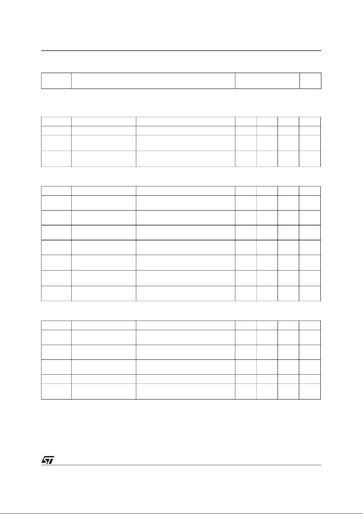
BLOCK DIAGRAM
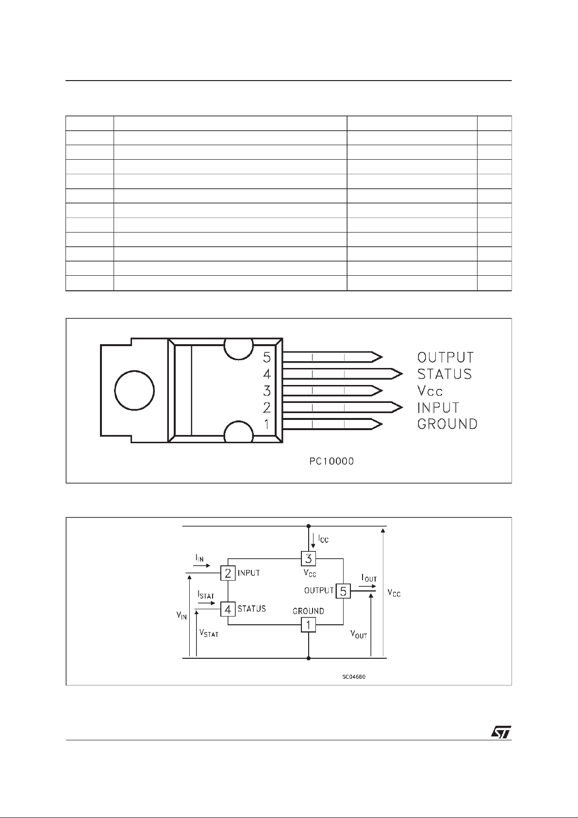
PENTAWATT
(vertical)
PENTAWATT
(horizontal)
PENTAWATT
(in-line)
ORDER CODES:
PENTAWATTvertical VN02H
PENTAWATThorizontal VN02H(011Y)
PENTAWATTin-line VN02H(012Y)
March 1999
1/10
Page 2
VN02H
ABSOLUTEMAXIMUMRATING
Symbol Parameter Value Unit
V
(BR)DSS
I
OUT
I
I
V
-V
I
STAT
V
ESD
P
T
T
CONNECTIONDIAGRAMS
Drain-S o ur ce Breakdown V olt age 60 V
Out put Cu r rent (cont. ) 6 A
Reverse Out put Current -6 A
R
Input Current ±10 mA
IN
Supply Voltage (for t = 400 ms) 60 V
CC
Reverse Supply V oltage -4 V
CC
St at us Cur rent ±10 mA
Elect r o st at ic Dischar ge (1.5 kΩ, 100 pF ) 2000 V
Power Dissipation at Tc≤ 25oC28W
tot
Junction O perat in g T em pe r at ure -40 t o 150
j
St orage Tem per atur e -55 t o 150
stg
o
C
o
C
CURRENT ANDVOLTAGECONVENTIONS
2/10
Page 3
VN02H
THERMALDATA
50
20
o
C/W
o
C/W
µA
mA
A/µs
A/µs
4
A/µs
R
thj-case
R
thj- amb
Ther mal Resis t an ce Junction- case Max
Therm al Resistanc e Junction-a m bient Max
4.4
60
ELECTRICAL CHARACTERISTICS (VCC=9 to 36 V; -40≤ Tj≤ 125oCunless otherwise specified)
POWER
Symbol Parameter Test C ondition s Min. Typ. Max. Unit
V
R
I
Supply Voltage see note 1 5 36 V
CC
On Stat e Resist a nce I
on
Supply Current Of f Stat e Tj≥ 25oC
S
=3A
OUT
=3A Tj=25oC
I
OUT
0.8
0.4
On State
SWITCHING
Symbol Parameter Test C ondition s Min. Typ. Max. Unit
t
d(on)
t
r
t
d(off)
t
f
(di/dt)
(di/dt)
V
demag
Turn-on Delay Time Of
Out put Cu r rent
Rise TimeOf Output
Current
Turn-off Delay Time Of
Out put Cu r rent
Fall T ime Of Output
Current
Tur n-on Current S lope I
on
Tur n-of f C urrent Slope I
off
Induc t i ve Load Clamp
Volt age
I
= 3 A Resis tive Load
OUT
Input Rise Time < 0.1 µsT
I
= 3 A Resis tive Load
OUT
Input Rise Time < 0.1 µsT
I
= 3 A Resis tive Load
OUT
Input Rise Time < 0.1 µsT
I
= 3 A Resis tive Load
OUT
Input Rise Time < 0.1 µsT
=3A
OUT
I
OUT=IOV
=3A
OUT
I
OUT=IOV
I
= 3 A L = 1 m H -7 -4 -2 V
OUT
25 ≤ Tj≤ 140oC
25 ≤ Tj≤ 140oC
=25oC
j
=25oC
j
=25oC
j
=25oC
j
51020µs
51545µs
51530µs
2615µs
0.05 0.15 0.52A/µs
0.1 0.4 2
Ω
Ω
LOGIC INPUT
Symbol Parameter Test C ondition s Min. Typ. Max. Unit
V
V
V
I(hyst.)
I
V
Input Low Level
IL
Volt age
Input Hig h Lev el
IH
2(*)V
Volt age
Input Hysteresis
0.5 V
Volt age
Input Current VIN= 5 V 250 5 00 µA
IN
Input Cla m p Volt ag e IIN=10mA
ICL
=-10mA
I
IN
5.5 6
-0.7 -0.3
0.8 V
V
V
3/10
Page 4

VN02H
ELECTRICAL CHARACTERISTICS (continued)
PROTECTION AND DIAGNOSTICS
Symbol Parameter Test C ondition s Min. Typ. Max. Unit
V
(•) Status V olt age Out put
STAT
V
USD
V
SCL
t
SC
I
OV
I
I
I
OUT
T
TSD
T
(*) The VIHis internallyclamped at6V about. Itis possible to connect this pin to an higher voltage via anexternal resistor calculated to not
exceed 10 mA at the input pin.
(•) Status determination > 100 µs after the switching edge.
Note 1 : AboveV
temperature reaches thermal shutdown temperature.
Low
Under Voltage Shut
Down
(•) Stat us Clam p Volt age I
Swit ch-off T im e in
Short Circ u it Condition
at Start-Up
Over Current R
Aver age Current in
AV
Short Circuit
Open Load Cur rent
OL
Level
Leakage Current Of f Stat e V
Ther mal Shut- d own
Tem perature
Reset Temperat u r e 125 145
R
= 36 V the outputvoltage is clamped to 36 V. Power dissipation increases and the device turnsoff ifjunction
CC
I
=1.6mA 0.4 V
STAT
2.5 5 V
=10mA
STAT
=-10mA
I
STAT
R
<10mΩ VCC=13V
LOAD
=25oC
T
c
<10mΩ VCC=13V 28 A
LOAD
R
<10mΩ VCC=13V
LOAD
=85oC
T
c
9< VCC<32V 5 70 mA
=0V 60 µA
OUT
5.5 6
-0.7 -0.3
1.5 5 ms
0.9 1.8 A
140 160
V
V
o
C
o
C
FUNCTIONALDESCRIPTION
The device has a diagnostic output which
indicates open circuit (no load) and over
temperature conditions. The output signals are
processedby internallogic.
To protect the device against short circuit and
over-current condition the thermal protection
turns the integratedPower MOSoff at a minimum
junction temperature of 140
temperaturereturns to about 125
o
C. When the
o
C theswitch is
automatically turned on again. To ensur the
protection in all V
conditions and in all the
CC
junction temperature range it is necessary to limit
the voltage drop across Drain and Source (pin 3
and 5) at 29 V. The device is able to withstanda
load dump according the test pulse 5 at level III of
the ISO TR/1 7631.
Above V
= 36V the output voltage is clamped
CC
to 36V. Power dissipation increases and the
device turns off if junction temperature reaches
thermalshutdowntemperature.
PROTECTING THE DEVICE AGAINST
REVERSEBATTERY
The simplest way to protect the device against a
continuous reverse battery voltage (-26V) is to
insert a Schottky diode between pin 1 (GND) and
ground, as shown in the typical application circuit
(fig. 3).
The consequences of the voltage drop across
this diode are as follows:
- If the input is pulled to power GND, a negative
voltage of -V
thresholds and V
respect to powerGND).
is seen by the device. (VIL,V
F
are increased by VFwith
STAT
IH
- The undervoltage shutdown level is increased
by V
.
F
If there is no need for the control unit to handle
external analog signals referred to the power
GND, the best approach is to connect the
reference potential of the control unit to node [1]
(see application circuit infig. 4), which becomes
the common signal GND for the whole control
board.
In this way no shift of V
IH,VIL
place and no negative voltage appears on the
INPUT pin; this solution allows the use of a
standard diode, with a breakdown voltage able to
handle any ISO normalized negative pulses that
occours in the automotiveenvironment.
and V
STAT
takes
4/10
Page 5

TRUTH TABLE
INPUT OUTPUT DIAGNOSTIC
Normal Opera ti on L
Open Circ uit (No Load) L
Ov er- temperature L
Under-voltage L
Figure1: Waveforms
VN02H
L
H
H
H
H
H
L
H
L
H
L
L
H
H
H
L
H
L
H
H
Figure2: Over Current Test Circuit
5/10
Page 6

VN02H
Figure3: TypicalApplicationCircuitWith A Schottky Diode For Reverse SupplyProtection
Figure4: TypicalApplicationCircuitWith Separate Signal Ground
6/10
Page 7

PENTAWATT (VERTICAL) MECHANICAL DATA
VN02H
DIM.
A 4.8 0.189
C 1.37 0.054
D 2.4 2.8 0.094 0.110
D1 1.2 1.35 0.047 0.053
E 0.35 0.55 0.014 0.022
F 0.8 1.05 0.031 0.041
F1 1 1.4 0.039 0.055
G 3.2 3.4 3.6 0.126 0.134 0.142
G1 6.6 6.8 7 0.260 0.268 0.276
H2 10.4 0.409
H3 10.05 10.4 0.396 0.409
L 17.85 0.703
L1 15.75 0.620
L2 21.4 0.843
L3 22.5 0.886
L5 2.6 3 0.102 0.118
L6 15.1 15.8 0.594 0.622
L7 6 6.6 0.236 0.260
M 4.5 0.177
M1 4 0.157
Dia 3.65 3.85 0.144 0.152
MIN. TYP. MAX. MIN. TYP. MAX.
mm inch
P010E
7/10
Page 8

VN02H
PENTAWATT (HORIZONTAL) MECHANICAL DATA
DIM.
MIN TYP MAX MIN TYP MAX
A 4.30 4.80 0.169 0.189
C 1.17 1.37 0.046 0.054
D 2.40 2.80 0.094 0.110
E 0.35 0.55 0.014 0.021
F 0.80 1.05 0.031 0.041
G 3.20 3.60 0.126 0.142
G1 6.60 7.00 0.260 0.275
H1 9.30 9.70 0.366 0.382
H2 10.40 0.409
H3 10.05 10.40 0.396 0.409
L2 14.60 15.20 0.575 0.598
L3 3.50 4.10 0.137 0.161
L5 2.60 3.00 0.102 0.118
L6 15.10 15.80 0.594 0.622
L7 6.00 6.60 0.236 0.260
V4 90
Diam. 3.65 3.85 0.144 0.151
mm inch
o
90
o
8/10
PO1OL1_E
Page 9

PENTAWATT(IN-LINE) MECHANICAL DATA
VN02H
DIM.
A 4.30 4.80 0.169 0.189
C 1.17 1.37 0.046 0.054
D 2.40 2.80 0.094 0.110
E 0.35 0.55 0.014 0.021
F 0.80 1.05 0.031 0.041
F2 1.10 1.40 0.043 0.055
F3 1.25 1.55 0.049 0.061
G 3.20 3.60 0.126 0.142
G1 6.60 7.00 0.260 0.275
H1 9.30 9.70 0.366 0.382
H2 10.40 0.409
H3 10.05 10.40 0.396 0.409
L2 23.05 23.80 0.907 0.937
L3 25.30 26.10 0.996 1.027
L4 0.90 2.90 0.035 0.114
L5 2.60 3.00 0.102 0.118
L6 15.10 15.80 0.594 0.622
L7 6.00 6.60 0.236 0.260
V4 90
Diam. 3.65 3.85 0.144 0.151
MIN TYP MAX MIN TYP MAX
mm inch
o
90
o
P010D
9/10
Page 10

VN02H
Information furnished is believed to beaccurate and reliable. However, STMicroelectronics assumes noresponsibility for the consequences
of use of such information nor for any infringement of patents or other rights of third parties which may result from its use. No license is
granted by implication or otherwise under any patent or patent rights of STMicroelectronics. Specification mentioned in this publication are
subject to change without notice. This publication supersedes and replaces all information previously supplied. STMicroelectronics products
are not authorized for use as critical components in life support devices or systems without express written approval of STMicroelectronics.
The ST logo is a trademark of STMicroelectronics
1999 STMicroelectronics – Printed in Italy – AllRights Reserved
STMicroelectronicsGROUP OF COMPANIES
Australia - Brazil -Canada - China -France -Germany - Italy-Japan - Korea - Malaysia - Malta - Mexico -Morocco -The Netherlands-
Singapore - Spain - Sweden - Switzerland - Taiwan -Thailand - UnitedKingdom - U.S.A.
http://www.st.com
.
10/10
 Loading...