

Page 1

®
VK05CFL
ELECTRONIC DRIVER FOR CFL APPLICATION
TYPE B
VK05CFL 520 V 0.25A 1.5A
■ EMITTER SWITCH POWER OUTPUT STAGE
■ INTEGRATED ANTIPARALLEL COLLECTOR
V
I
Crms
I
Peak
SOURCE DIODE
■ INTEGRATED DIAC FUNCTION
■ NOMINAL WORKING FREQUENCY
SETTABLE BY EXTERNAL CAPACI TO R
■ IGNITION FREQUENCY SET BY LOAD
DESCRIPTION
The VK05CFL is a m onolithic devi ce housed in a
standard SO-8 package, made by using
STMicroelectronics proprietary VIPower M3
Technology. T his device is intended both for the
low side and the high side driver in half bridge CFL
applications. This means that it is possible to
realize a complete H-bridge by using two
VK05CFL devices: one connected in HSD
configuration and the other connected in LSD
configuration. In the VK05CFL used in HSD
BLOCK DIAGRAM
SO-8
configuration, the diac pin must be connected to
source pin. B oth diac fu nctionality and disch arge
circuit for ext ernal diac capacitor are integrated.
By an external capac itor it is possible to choose
the nominal working fre quency without influence
on the ignition one.
Collector
diac
Diac
sec
osc
2Vref
R
5Vref
Septe m ber 2002 1/14
-
+
+
-
Source
Page 2
VK05CFL
ABSOLUTE MAXIMUM RATING
Symbol Parameter Min Typ Max Unit
V
CS
I
sec
V
sec
I
CM
I
OSC
V
OSC
T
j
T
stg
THERMAL DATA
Symbol Parameter Value Unit
R
thj-lead
R
thj-amb
(*) When mounted on a standard single-sided FR-4 board with 100m m2 of Cu (at leas t 35µ m t hick).
CONNECTION DIAGRAM
Collector-Source Voltage 520 V
Input Current (sec ondary) -100 140 mA
Input Voltage (secondary) Internally limited V
Collector Peak Current -1.8 1.8 A
Osc Pin Current 100 mA
Osc Pin Voltage Internally limited V
Max Operating Junction Temperature -40 150 °C
Storage Temperature Range -55 150 °C
Thermal Resistance Junction - lead Max 15 °C/W
Thermal Resistance Junction - ambient Max 52 (*) °C/W
Collector
Collector
Collector
Collector
5
8
4
sec
osc
diac
1
Source
SO-8
PIN FUNCTIONS
Pin Name Pin Function
Collector Collector of the NPN high voltage transistor in the cascode configuration.
Sour ce Low vol ta ge Power MOSF ET source in th e cascode configurati o n and GROUND re f e ren ce.
diac Input of t he diac block t o start the s ystem up at the beginning.
sec
osc Output via to cha rge external capacitor necessary to set the steady state working frequency.
Connection with secondary winding of the voltage transformer, in order to trigger and to supply the
device.
2/14
Page 3
VK05CFL
ELECTRICAL CHARACTERISTICS (T
=25°C unless otherwise specified)
case
FORWARD
Symbol Parameter Test Conditions Min Typ Max Unit
V
CS(sat)
Collector-Source Saturation Voltage V
=10V; IC=300mA 1.4 2.8
sec
REVERSE
Symbol Parameter Test Conditions Min Typ Max Unit
V
Collector-Source Reverse Voltage IC= -300mA -1 -1.5
CSr
OSC
Symbol Parameter Test Conditions Min Typ Max Unit
I
OSC
V
OSC(th)
Osc Output Current V
Osc Turn-off Voltage V
=10V; V
sec
=10V 1. 6 2
sec
=0V 300 µ
OSC
DIAC
Symbol Parameter Test Conditions Min Typ Max Unit
V
diac(thH)
V
diac(thL)
Diac On Threshold 28 31 35
Diac Off Threshold 18
SEC
Symbol Parameter Test Conditions Min Typ Max Unit
V
sec(clH)
V
sec(clL)
V
sec(on)
I
sec(on)
Sec Clamp Hig h I
Sec Clamp Low I
Sec Turn-on Voltage IC=10mA; V
Sec On Current
=20mA; V
sec
= -10mA 25
sec
V
=10V; V
sec
IC=300mA
=0V 22
OSC
=0V 3.5 4.5 5.5
OSC
=0V;
OSC
4
V
V
A
V
V
V
V
V
V
mA
3/14
Page 4
VK05CFL
APPLICATION DESCRIPTION
Technology Overview
The VK05CFL is made by using STMicroelectronics proprietary VIPower M3-3 technology. This
technology allows the integration in the same chip both of the control part and the power stage. The power
stage is the “Emitter Switching”. It is ma de by putting in cascode co nfiguration a bipolar high voltage
darlington with a low voltage MOSFET. This configuration provides a good trade-off between the bipolars
low ON drop wi th high break down vo ltage in OFF sta te, and the M OSFETS hi gh swi tchin g speed. The
maximum theoretical working frequency is in the range of 300KHz.
Circuit description
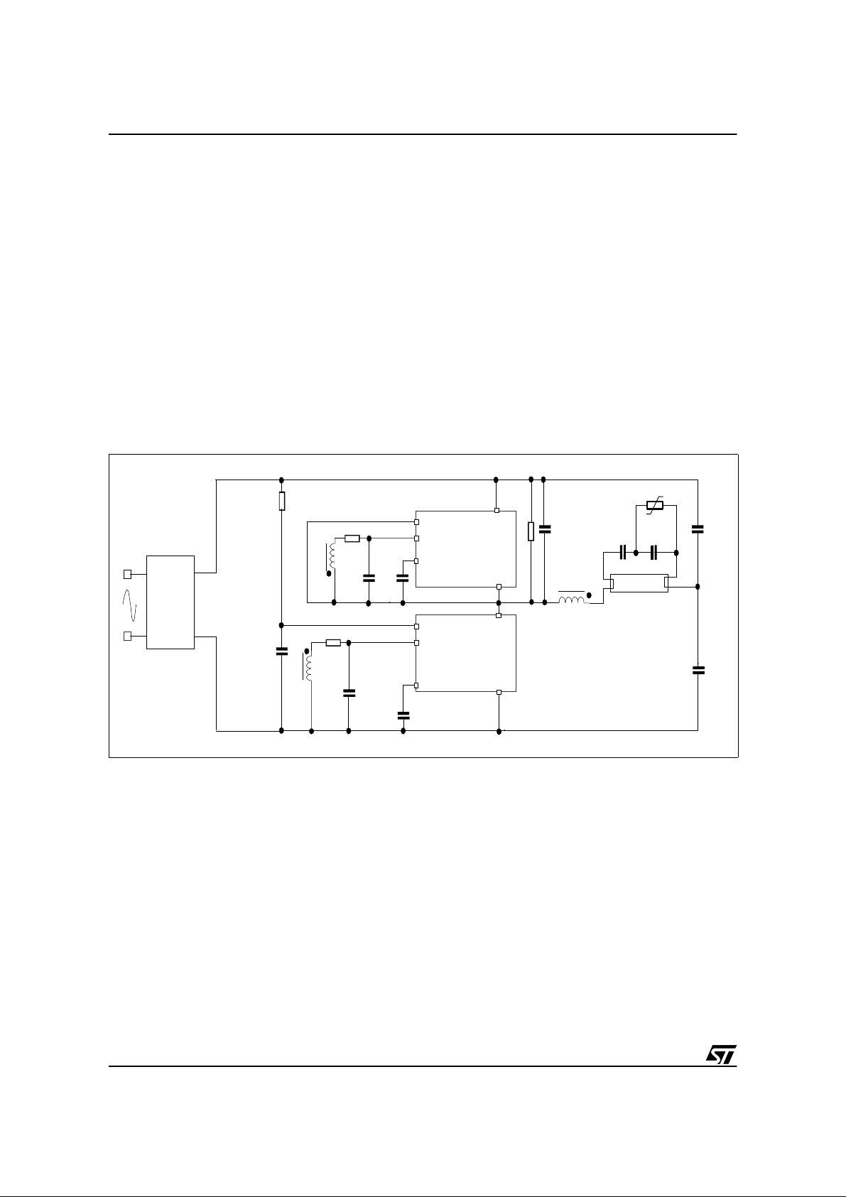
The electrica l scheme of the VK05CFL used as a self- oscillating c onverter to drive fluor escent tubes is
shown in Fig. 1.
Figur e 1: Application schematic
PTC
C4 C13
Tube
C2
Bridge
+
Inpu t F ilte r
R2
diac
sec
R4
L1s
C10
C8
R5
L2s
C11
C5
osc
diac
sec
VK05CFL
osc
C6
VK05CFL
Collector
Source
C ollector
Source
C7 C3
R1
Lp
This topology does not req uire the sat urable trans former to set t he working fre quency. Two secondary
windings are wound on the main ballast choke Lp. These windings have two functions:1) to trigger the ON
state and 2) to provide the power supply to the device. A good trade-off for the ratio between the primary
winding Lp and the two se condary windings i s 10:1; in ord er to minimize th e power dissip ated on the
resistors R4 - R5 and to guarantee sufficient voltage to supply the device.
The steady-state working frequency is set by the two capacitor C5 and C6. They are charged by a current
I
≈300µA. When the voltage on the capacitor reaches an internal fixed value the power stage is turned
cap
OFF. By choosing the same value for C5 and C6 the circuit will work with a duty-cycle of 50%. During the
start-up, as the res onance freq uency is hig her than the steady- state freq uency, the s econdary vol tage
falls lower than the device sustain voltage before the capacitor C5-6 is charged, switching OFF the device.
For this reason t he circui t can wo rk at different frequencies dur ing the start-up and steady-s t ate pha ses .
The resistor R 2 an d the cap ac itor C 8 a re nee ded to bias the int erna l d iac in the low side de v ice i n orde r
to start-up the system. In the high side d evice the diac pin must be connected to the midp oint. R1 is the
pull-up resistor and C7 is the snubber capacitor.
Input filt ering i s r eali zed by R 4-C10 and R5-C11. I t is necess ar y to ha ve a proper supp ly voltage on the
input pin.
4/14
1
Page 5
VK05CFL
f
st up–
1
2π LcC4⋅
------------ -----------------
=
Functional description
When the circuit is supplied, the capacitor C8 is charged by the resistor R2 till the voltage across it
reaches the internal d iac thresho ld value (~ 30V). The l ow side swi tch is tu rned ON and c onsequently
current will flow from the HV rail to ground through the path formed by C3//C2, C4 and Lp (in case that the
pre-heating network is not present: PTC and C13 are not connected). The voltage drop on Lp is
“transferred” to the two secondary windings (wound in opposition) in order to confirm the ON state for the
low side device and the OFF state for the high side device. As soon as the low side device switches ON,
the capacitor C8 is discharged to ground by an internal HV diode to avoid diac restart.
In this preliminary phase the tube is OFF and the circu it will oscillate at the Lp-C4 series with (C3//C2)
resonance frequency
we can neglect C3//C2
As this frequency is higher than the steady-state one, the two devices will switch ON-OFF at this
frequency, as t he voltage on the tw o secondary windings fall s below the voltage need ed to keep the
device on.
As soon as the tube is ign it ed the r esonan c e freq uency i s red uced ≈(Lp-C3//C2) and the circuit will work
at the steady-state frequency fixed by the two capacitors C5 and C6.
It is possible to calculate the steady-state frequency by these formulae:
5
T
on
RC
-- -
ln⋅⋅=
2
(R = internal impedance)
1
-- -
TTont
2
f
=
Considering th e V K 05CFL bo ard: R =1 2KΩ; C5=C6=1.2nF ; t
the working frequency will be: f≈35KHz.
++=
1
--T
storagetdv()dt()⁄
≈400nsec; C 7= 680p F⇒t
storage
(dv)/(dt)
≈800nsec;
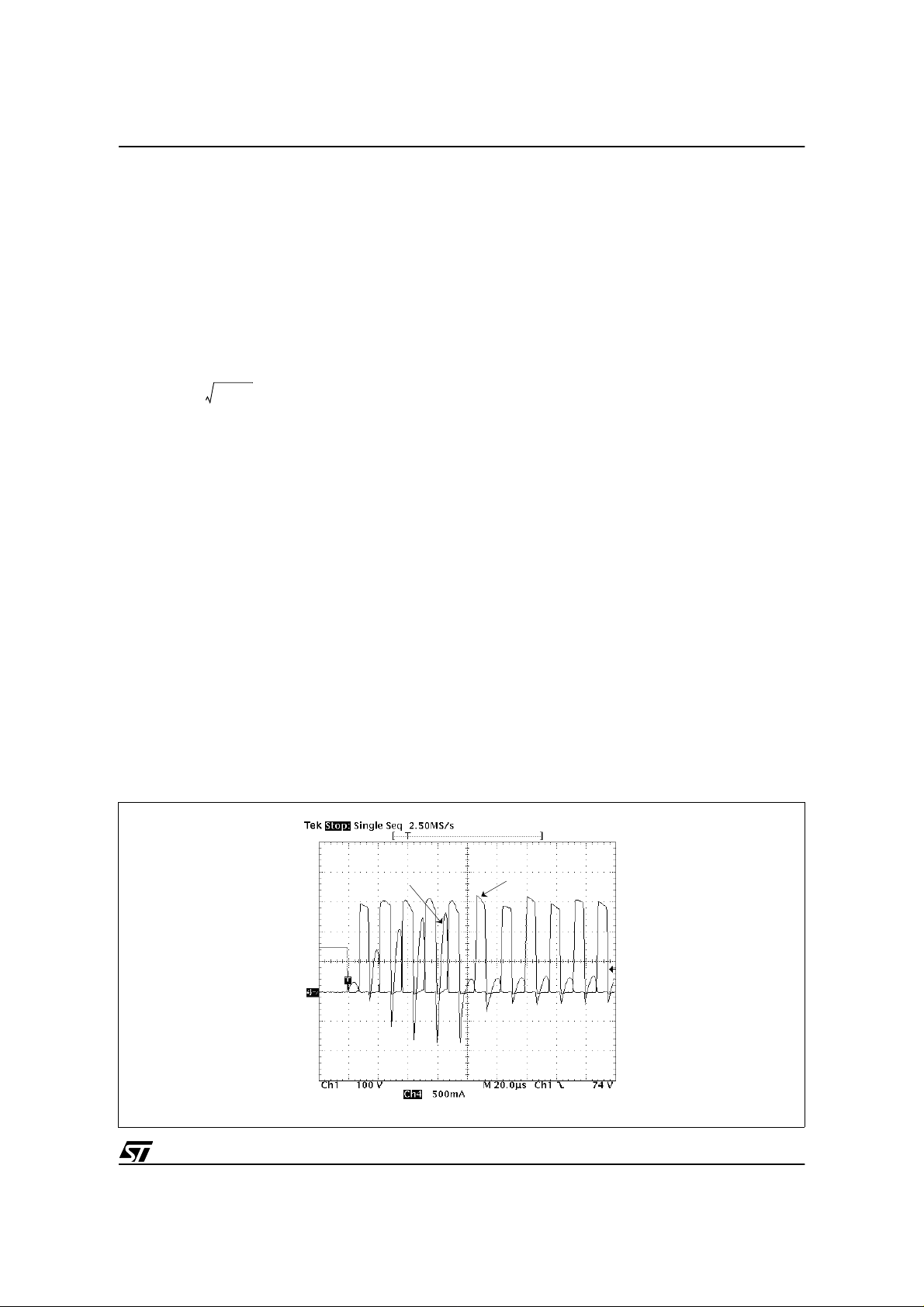
In figure 2 and figure 3, the start-up phase without preheating is reported , while in figure 4 the main
waveforms in steady-state are shown.
Figur e 2: Start-up phase
midpoint
device
I
5/14
Page 6

VK05CFL
midpoint
Figur e 3: Start-up phase
diac
midpoint
From figure 4 it can be observe d that the v alue of se conda ry voltag e decreases when th e lamp current
increases. This happens because in creasing t he value of the cu rrent flowin g through the tube, incre ase
the drop on it, consequently decreasing the voltage on the ballast inductor Lp and thereby decreasing also
the secondary voltage.
By inserting the filters (R4-C10; R5-C11) between the two secondary windings and the devices, it is
possible to guarantee a h igher voltage on the inp ut pin of the de vices for l onger time comp ared to t he
secondary signal. In this way it is possible to extend the use of the VK05CFL to all the power range eg.5W
– 23W.
Figur e 4: Steady state waveforms
6/14
V
L2s
V
sec
V
Ip
Page 7

VK05CFL
Secondary Filter Design
The design of RC ne twork app l ied on the sec pin of both de vic es has to be do ne taki ng into acc oun t the
following considerations:
1) The sec filtered voltage must reach the device ON threshold at the end of the negative dV/dt and before
the end of the freewheeling diode conduction in order to avoid hard switching or switching ON delay.
2) The filtered voltage must be high enough (greater than 5V) at the end of Ton in order to guarantee the
device supply voltage.
A good choice for time constant (τ=RC) is in the range:1.5 µs ÷ 3.3 µs.
The resistor value has chosen in relation to the power dissipated on it during the start-up phase, the worst
condition is verified when the preheating is used.
Tube p r e-heati ng
By using the VK05CFL, the tube pre-heating can be done with the classical solution with PTC (see
application schematic i n figure 1) or with a more r eliable low voltage networ k (see figure 5b). The pre heating low voltage network allows to obtain an optimum pre-heating avoiding the overstress on the PTC
thus improving the ballast reliability and the lamp life-time.
Figure 5a: Pre-heating phase with PTC
I
lamp
Figur e 5b: Pre-heating low voltage network
sec
1M
1M
39K
+
1.2n
39K
+
1.2n
10µ
10µ
Iosc
I
osc
VK05CFL
High side
osc
sec
VK05CFL
Low side
osc
APPLICATION BOARD
Please no te that this demo can be u sed for Europ e (230Vrms) market as well as for USA ( 110Vrms)
market.
In order to use the demoboard for Euro pe market th e followi ng modificatio n must be done: ele ctrolytic
capacitors C1 and C12 must be replaced with only one electrolytic capacitor Cx = 3,3µF/400V connected
with the positive pi n on the D1 cato de and the negati ve pin on the D 3 anode . Also diffe rent po w er ran ge
CFL can be driven by using this demoboard; on the left side of the component list reported below you find
component val ues able to drive CFL in the power ran ge 5W to 15W, the compo nent values writte n in
brackets in the table on the right are referred to the power range 15W to 23W.
7/14
Page 8

VK05CFL
COMPONENT L IST
5W to 15W lamp
Reference Value
T1 Lp=3,1mH, N1/N2=N1/N3=10
L
0
D0,D1,D2, D 3 1N4007
C1, C12
C2, C3 100nF/250V
C4 2,4nF/400V
C5, C6 1.2nF/63V
C7 470pF/400 V
C8 22nF/100V
C10, C1 1 1.5nF/1 00V
R0 10Ω 1/2W
R1, R2 1MΩ 1/4W
R4, R5 2.2KΩ 1/ 4W
U1, U2 VK05CFL
820µH
22µF/200 V electrolytic
(for Europe to replace C1, C12 with
Cx=3,3µF/400V)
>15W to 23W lamp
Referenc e Value
T1 Lp=2,1mH, N1/N2=N1/N3=10
L
0
D0,D1,D2, D 3 1N4007
C1, C12
C2, C3 100nF/250V
C4 2,4nF/400V
C5, C6 1nF/63V
C7 470pF/400V
C8 22nF/100V
C10, C11 1.5nF/100V
R0 10Ω 1/2W
R1, R2 1MΩ 1/4W
R4, R5 1KΩ 1/2W
U1, U2 VK05CFL
820µH
22µF/200V electrolytic
(for Europe Cx=6.8µF/400V)
Waveforms below was obtained by using the application demoboard mounted for european market:
Device ∆T (T
=25 °C) for different power lamps
amb
Device power dissipation Vs. power lamp
8/14
Page 9

D0 D1
C12
L0
C3
R4
8
R2
87 56
VK05CFL
1234
Figur e 6: Board electrical scheme
U1
R1C7
3
220V ~
2
110V ~
1
R0
D2 D3
C1
C2
C4
36
1
T1
2
C10
R5
C11
8765
VK05CFL
1342
C8
C5
U2
C6
VK05CFL
9/14
Page 10

VK05CFL
Figur e 7: Printed Circuit Board legend (Component side)
Figur e 8: Printed Circuit Board top foil
10/14
Page 11

VK05CFL
Collector current Vs. collector-source saturation
voltage at T
amb
=25ºC
Vsec = 15V
Vsec = 10V
Vsec = 6V
Freewheeling diode If=f(Vf) characteristic at
T
=25ºC
amb
T = 25°C
Collector current Vs. collector-source saturation
voltage at T
amb
=125ºC
Vsec = 15V
Vsec = 10V
Vsec = 6V
Freewheeling diode If=f(Vf) characteristic at
T
=125ºC
amb
T = 125°C
Bipolar storage time Vs. collector current
Test circuit
11/14
Page 12

VK05CFL
SO-8 MECHANICAL DATA
DIM.
A 1.75 0.068
a1 0.1 0.25 0.003 0.009
a2 1.65 0.064
a3 0.65 0.85 0.025 0.033
b 0.35 0.48 0.013 0.018
b1 0.19 0.25 0.007 0.010
C 0.25 0.5 0.010 0.019
c1 45 (typ.)
D 4.8 5 0.188 0.196
E
e 1.27 0.050
e3 3.81 0.150
F 3.8 4 0.14 0.157
L 0.4 1.27 0.015 0.050
M 0.6 0.023
S 8 (max.)
L1 0.8 1.2 0.031 0.047
MIN. TYP MAX. MIN. TYP. MAX.
5.8
mm. inch
6.2 0.228 0.244
12/14
Page 13

SO-8 TUBE SHIPMENT (no suffix)
VK05CFL
B
C
Base Q.ty 100
Bulk Q.ty 2000
Tube length (± 0.5) 532
A
A 3.2
B 6
C (± 0.1) 0.6
All dimensions are i n m m .
TAPE AND REEL SHIPMENT (suffix “13TR”)
REEL DIMENSIONS
Base Q.ty 2500
Bulk Q.ty 2500
A (max) 330
B (min) 1.5
C (± 0.2) 13
F 20.2
G (+ 2 / -0) 12.4
N (min) 60
T (max) 18.4
All dimensions are i n m m .
TAPE DIMENSIONS
According to Electronic Industries Asso ciation
(EIA) Sta ndard 481 rev. A, Feb. 1986
Tape width W 12
Tape Hole Spacing P0 (± 0.1) 4
Component Spacing P 8
Hole Diameter D (± 0.1/-0) 1.5
Hole Diameter D1 (min) 1.5
Hole Position F (± 0.05) 5.5
Compartment Depth K (max) 4.5
Hole Spacing P1 (± 0.1) 2
All dimensions are i n m m .
Top
cover
tape
End
500mm min
Empty components pockets
saled with cover tape.
User direction of feed
Start
No componentsNo components Components
500mm min
13/14
Page 14

VK05CFL
Information furnished is believed to be ac c ur ate and reliab le. However, STMicroelectronics as s um es no responsibility for the consequences
of use of such information nor for any infringement of patents or other rights of third parties which may results from its use. No license is
granted by implication or otherwise under any patent or patent r ights of STMicroelectronics . Specificatio ns m entioned in this publication are
subject to c hange without notice. This publicatio n s upersedes an d r eplaces all information p r ev iously suppl ied. STMicroelectronic s pr oducts
are not authorized for use as critical components in life support devices or systems without express written approval of STMicroelectronics.
Australia - Brazil - Canada - China - Finland - Franc e - Germany - Hong Kong - India - Israel - Italy - Japan - M alaysia -
Malta - Morocco - Singapore - Spain - Sweden - Switzerland - United Kingdom - U.S.A.
The ST logo is a trademark of ST M ic r oelectronics
2002 STMicroelectronics - Printed in ITALY- All Rights Reserved.
STMicroelectronics GROUP OF COMPANIES
http://www.st.com
14/14
 Loading...