

Page 1
现货库存、技术资料、百科信息、热点资讯,精彩尽在鼎好!
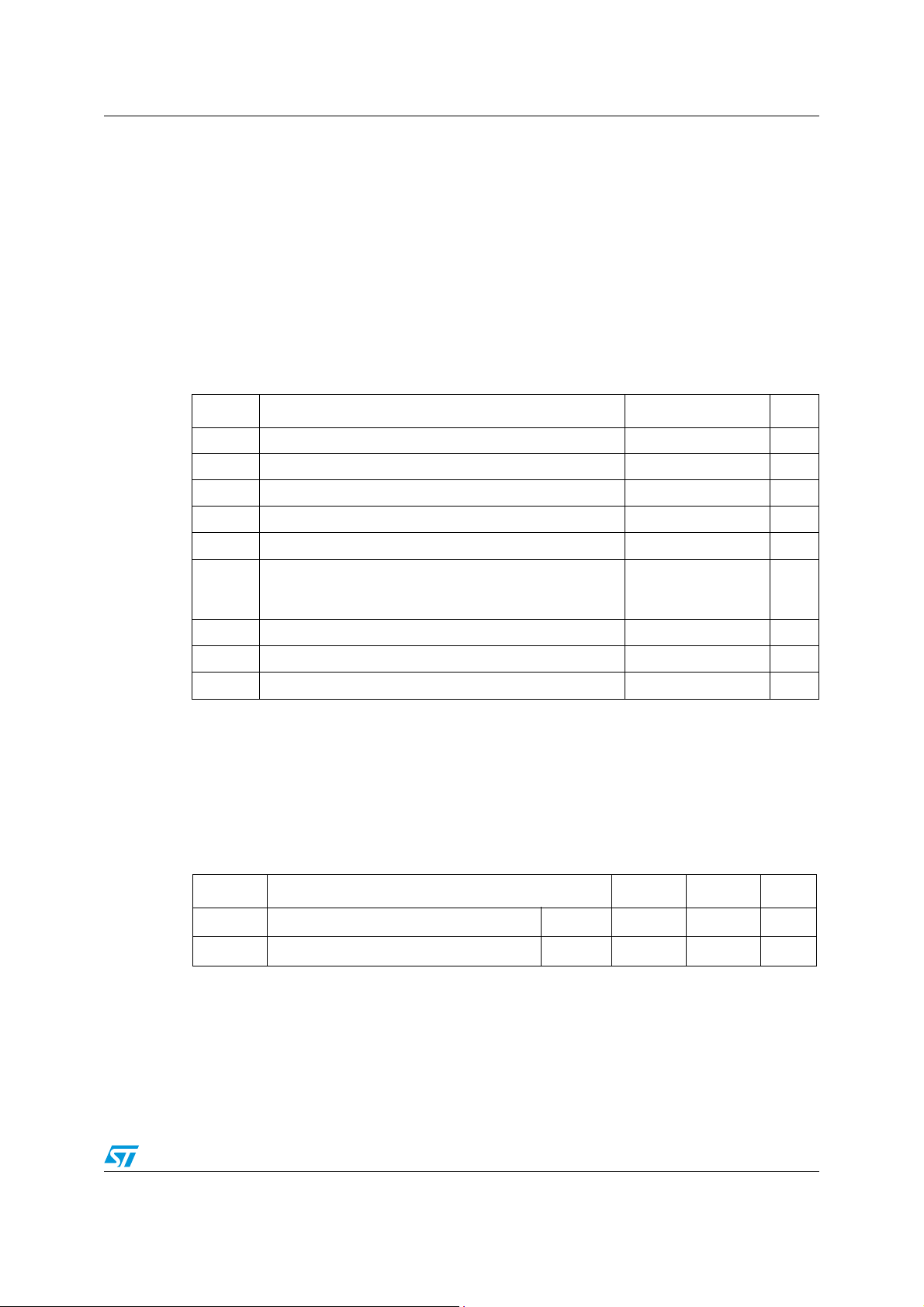
Low Power OFF-Line SMPS Primary Switcher
Features
■ Fixed 60kHZ Switching Frequency
■ 9V to 38V Wide Range V
■ Current Mode Control
■ Auxiliary Undervoltage Lockout with Hysteresis
■ High Voltage Start-up Current Source
■ Overtemperature, Overcurrent and
Overvoltage Protection with Auto-Restart
Typical Power Capability
Voltage
DD
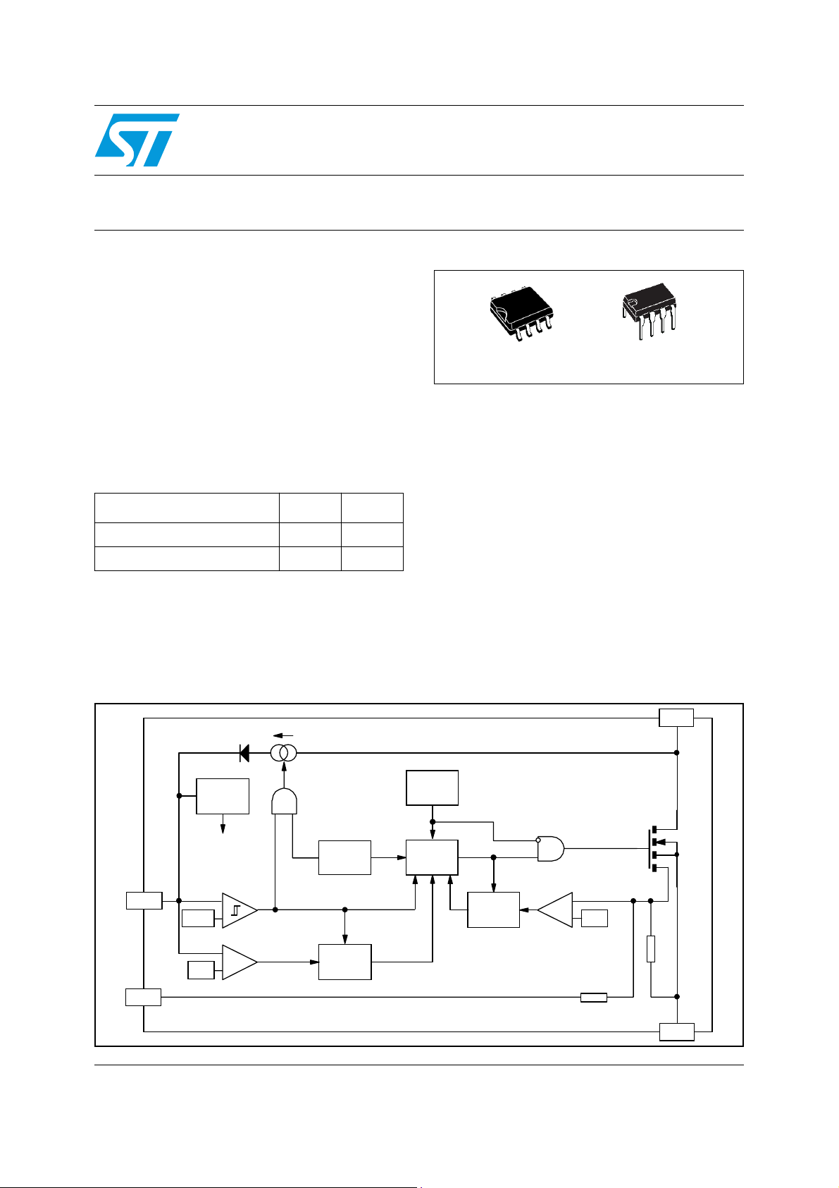
VIPer22ADIP - E
VIPer22AS - E
DIP-8SO-8
Description
The VIPer22A-E combines a dedicated current
mode PWM controller with a high voltage Power
MOSFET on the same silicon chip.
Mains type SO-8 DIP-8
European (195 - 265 Vac) 12W 20W
US / Wide range (85 - 265 V ac ) 7W 12W
Block diagram
ON/OFF
REGULATOR
INTERNAL
VDD
FB
8/14.5V
42V
SUPPLY
_
+
+
_
OVERTEMP.
DETECTOR
R
FF
S
OVERVOLTAGE
Q
LATCH
Typical applications cover off line power supplies
for battery charger adapters, standby power
supplies for TV or monitors, auxiliary supplies for
motor control, etc. The internal control circuit
offers the following benefits:
– L arge input voltage range on the V
accommodates changes in auxiliary supply
voltage. This feature is well adapted to
battery charger adapter configurations.
– Automatic burst mode in low load condition.
– Overvoltage protection in HICCUP mode.
DRAIN
60kHz
OSCILLATOR
PWM
S
LATCH
FF
R1
R4QR3
R2
BLANKING
+
_
0.23 V
Ω
230
Ω
1 k
DD
pin
SOURCE
February 2006 Rev1 1/20
www.st.com
20
Page 2

Contents VIPer22ADIP/ VIPer22AS - E
Contents
1 Electrical Data . . . . . . . . . . . . . . . . . . . . . . . . . . . . . . . . . . . . . . . . . . . . . . 3
1.1 Ma ximum Ratings . . . . . . . . . . . . . . . . . . . . . . . . . . . . . . . . . . . . . . . . . . . . 3
1.2 Th ermal Data . . . . . . . . . . . . . . . . . . . . . . . . . . . . . . . . . . . . . . . . . . . . . . . 3
2 Electrical Characteristics . . . . . . . . . . . . . . . . . . . . . . . . . . . . . . . . . . . . . 4
3 Pin Connections and Function . . . . . . . . . . . . . . . . . . . . . . . . . . . . . . . . 6
4 Operations . . . . . . . . . . . . . . . . . . . . . . . . . . . . . . . . . . . . . . . . . . . . . . . . . 7
4.1 Re ctangular U-I Output Characteristics . . . . . . . . . . . . . . . . . . . . . . . . . . . 7
4.2 Wide Range of VDD Voltage . . . . . . . . . . . . . . . . . . . . . . . . . . . . . . . . . . . 7
4.3 Fe edback Pin Principle of Operation . . . . . . . . . . . . . . . . . . . . . . . . . . . . . 8
4.4 Startup sequence . . . . . . . . . . . . . . . . . . . . . . . . . . . . . . . . . . . . . . . . . . . 10
4.5 O vervoltage threshold . . . . . . . . . . . . . . . . . . . . . . . . . . . . . . . . . . . . . . . .11
5 Operation pictures . . . . . . . . . . . . . . . . . . . . . . . . . . . . . . . . . . . . . . . . . 12
6 Mechanical Data . . . . . . . . . . . . . . . . . . . . . . . . . . . . . . . . . . . . . . . . . . . 15
7 Order codes . . . . . . . . . . . . . . . . . . . . . . . . . . . . . . . . . . . . . . . . . . . . . . . 18
8 Revision history . . . . . . . . . . . . . . . . . . . . . . . . . . . . . . . . . . . . . . . . . . . 19
2/20 Rev1
Page 3
VIPer22ADIP/ VIPer22AS - E Electrical Data
1 Electrical Data
1.1 Maximum Ratings
Stressing the device above the rating listed in the “Absolute Maximum Ratings” table may
cause permanent damage to the device. These are stress ratings only and operation of the
device at these or any other conditions above those indicated in the Operating sections of
this specification is not implied. Exposure to Absolute Maximum Rating conditions for
extended periods may affect device reliability. Refer also to the STMicroelectronics SURE
Program and other relevant quality documents.
Table 1. Absolute Maximum Rating
Symbol Parameter Value Unit
(2)
(1)
-0.3 ... 730 V
-0.3 ... 400 V
200
1.5
V
kV
V
Switching drain source voltage (TJ = 25 ... 125°C)
DS(sw)
V
St art-up drain source voltage (TJ = 25 ... 125°C)
DS(st)
I
Continuous drain current Internally limited A
D
V
Supply voltag e 0 ... 50 V
DD
I
Feedback current 3 mA
FB
Electrostatic discharge:
V
Machine model (R = 0Ω; C = 200pF)
ESD
Charged device model
T
Junction operating temperat ure Internally limited °C
J
T
Case operating temperature -40 to 150 °C
C
T
1. This parameter applies when the start-up current source is OFF. This is the case when the VDD voltage
has reached V
2. This parameter applies when the start up current source is on. This is the case when the VDD voltage has
not yet reached V
Storage Temperature -55 to 150 °C
stg
DDon
DDon
1.2 Thermal Data
Table 2. Thermal Data
Symbol Parameter SO-8 DIP-8 Unit
R
thJC
R
thJA
1. When mounted on a standard single-sided FR4 board with 200 mm2 of Cu (at least 35 µm thick)
connec te d to all DRAIN pin s.
Thermal Resist ance Junction - Case Max 25 15 °C/W
Thermal Resist ance Junction - Ambient
and remai ns abo v e V
or has fallen bel ow V
DDoff
.
DDoff.
(1)
Max 55 45 °C/W
Rev1 3/20
Page 4
Electrical Characteristics VIPer22ADIP/ VIPer22AS - E
2 Electrical Characteristics
TJ = 25°C, V
= 18V, unless otherwise specified
DD
Table 3. Power section
Symbol Parameter Test conditions Min. Typ. Max. Unit
BV
Drain-source voltage ID = 1mA; V
DSS
I
DSS
r
DS(on)
C
1. On cl amped inductive load
OFF State drain
current
Static drain-source
ON state resistance
t
Fall time
f
Rise time
t
r
Drain capacitance V
OSS
V
= 500V; V
DS
T
= 125°C
J
= 0.4A
I
D
I
= 0.4A; TJ = 100°C
D
= 0.2A; V
I
D
(See Figure 8 on page12)
= 0.4A; V
I
D
(See Figure 8 on page12)
= 25V 40 pF
DS
= 2V 730 V
FB
= 2V;
FB
0.1 mA
15 17
31
= 300V
IN
= 300V
IN
(1)
100 ns
(1)
50 ns
Ω
Table 4. Supply section
Symbol Parameter Test conditions Min. Typ. Max. Unit
I
DDch
St art-up charging
current
V
= 100V; V
DS
= 0V ...V
DD
(See Figure 9 on page 12)
DDon
-1 mA
St art-up charging
I
DDoff
current in thermal
shutdown
Operating supply
I
DD0
I
DD1
D
V
DDoff
V
DDon
V
DDhyst
V
DDovp
1. These test conditions obtained with a resistive load are leading to the maximum conduction time of the
device.
current not switching
Operating supply
current switching
Restart duty-cycle (See Figure 10 on page 12) 16 %
RST
Undervoltage
V
DD
shutdown threshold
Start-up
V
DD
threshold
Threshold
V
DD
hysteresis
Overvoltage
V
DD
threshold
= 5V; VDS = 100V
V
DD
T
> TSD - T
J
I
= 2mA 3 5 mA
FB
I
= 0.5mA; ID = 50mA
FB
HYST
(1)
(See Figure 9,
Figure 10 on page 12)
(See Figure 9,
Figure 10 on page 12))
0 mA
4.5 mA
7 8 9 V
13 14.5 16 V
(See Figure 9 on page 12) 5.8 6.5 7.2 V
38 42 46 V
4/20 Rev1
Page 5

VIPer22ADIP/ VIPer22AS - E E lectrica l Characteristics
Tabl e 5. Oscillation section
Symbol Parameter Test conditions Min. Typ. Max. Unit
F
Oscillato r fr equency
OSC
total var iat ion
V
= V
DD
T
DDoff
= 0 ... 100°C
J
... 35V;
54 60 66 kHz
Table 6. PWM Comparator section
Symbol Parameter Test Conditions Min. Typ. Max. Unit
G
I
ID
I
Dlim
I
FBsd
R
FB
t
d
t
Blanking time 500 ns
b
t
ONmin
to ID current gai n (See Figure 11 on page 13) 560
FB
Peak current
limitation
I
Shutdown current (See Figure 11 on page 13) 0.9 mA
FB
FB Pin input
impedance
Current sense del ay
to turn-OFF
Minimum Turn-ON
time
= 0V
V
FB
(See Figure 11 on page 13)
= 0mA
I
D
(See Figure 11 on page 13)
I
= 0.4A 200 ns
D
0.56 0.7 0.84 A
1.2 kΩ
700 ns
Tabl e 7. Overtemperature section
Symbol Parameter Test Conditions Min. Typ. Max. Unit
Thermal shutdown
T
SD
temperature
T
HYST
Thermal shutdown
hysteresis
Tabl e 8. Typical Power Capability
(See Figure 12 on page 13) 140 170 °C
(See Figure 12 on page 13) 40 °C
(1)
Mains type SO-8 DIP-8
European (195 - 265 Vac) 12W 20W
US / Wide range (85 - 265 Vac) 7W 12W
1. Above power capabilities are given under ad equate thermal condit ions
Rev1 5/20
Page 6
Pin Connectio ns and Function VIPer22ADIP/ VIPer22AS - E
3 Pin Connections and Function
Figure 1. Pin connection
SOURCE
SOURCE
FB
VDD
1
2
3
4
8
7
6
5
DRAIN
DRAIN
DRAIN
DRAIN
SO-8 DIP-8
Figure 2. Current and voltage conventions
I
DD
I
FB
V
DD
V
FB
VDD DRAIN
FB
CONTROL
VIPer22A
SOURCE
SOURCE
SOURCE
FB
VDD
1
2
3
4
I
D
V
D
8
DRAIN
7
DRAIN
6
DRAIN
5
DRAIN
Table 9. P in func tion
Pin Name Pin Function
Power supply of the control circuits. Also provides a charging current during start up
thanks to a high voltage current source connected to the drain. For this purpose, an
hysteresis comparator monitors the V
V
DD
SOURCE Power MOSFET source and circuit gr ound reference.
DRAIN
FB
6/20 Rev1
: V oltage value (typically 14.5V) at which the devi ce starts swit ching and turns
- V
DDon
off the start up current source.
- V
: Voltage value (typically 8V) at which the device stops switching and turns on
DDoff
the start up current source.
Power MOSFET drain. Also used by the internal high voltage current source during
start up phase for charging the external V
Feedback input. The useful volt age ran ge ex tends f rom 0V to 1V, and defines th e peak
drain MOSFET current. The current limitation, which corresponds to the maximum
drain current, is obtained for a FB pin shorted to the SOURCE pin.
voltage and provides two thresholds:
DD
capacitor.
DD
Page 7

VIPer22ADIP/ VIPer22AS - E Operations
A
T
4 Operations
4.1 Rectangular U-I Output Characteristics
Figure 3. Rectangular U-I output characteristics for battery charger
C IN
R1
C2
D1
F1
T2
C3
D4
C4
-+
ISO1
U1
C5
C10
FB
C6
VIPerX2A
R7R5R8
R10
D3
VDD DRAIN
CONTROL
SOURCE
R2
U2
R3
C8
TSM101
Vcc
Vref
-
+
GND
T1
C7
D5
+
-
C1
D2
R4
C9
DCOU
R6
R9
GND
A complete regulation scheme can achieve combined and accurate output characteristics.
Figure 3. presents a secondary feedback through an optocoupler driven by a TSM101. This
device offers two operational amplifiers and a voltage reference, thus allowing the regulation
of both output voltage and current. An integrated OR function performs the combination of
the two resulting error signals, leading to a dual voltage and current limitation, known as a
rectangular output characteristic. This type of power supply is especially useful for battery
chargers where the output is mainly used in current mode, in order to deliver a defined
charging rate. The accurate voltage regulation is also convenient for Li-ion batteries which
require both modes of operation.
4.2 Wide Range of VDD Voltage
The VDD pin voltage range extends from 9V to 38V. This feature offers a great flexibility in
design to achieve various behaviors. In
chosen to supply the device with two benefits:
Figure 3 on page7 a forward configuration has been
Rev1 7/20
Page 8

Operations VIPer 2 2ADIP/ VIPer22AS - E
■ As soon as the device starts switching, it immediately receives some energy from the
auxiliary winding. C5 can be therefore reduc ed and a smal l ceramic c hip (100nF) is
sufficient to insure the filtering function. The total s tart up time from the switch on of input
voltage to output voltage presence is dramatically decreased.
■ The output current characteristic can be maintained even with very low or zero output
voltage. Since the TSM101 is also supplied in forward mode, it keeps the current
regulation up whatever the output voltage is.The V
pin voltage may vary as much as
DD
the input voltage, that is to say with a ratio of about 4 for a wide range application.
4.3 Feedback P in Prin ciple of Ope ratio n
A feedback pin controls the operation of the device. Unlike conventional PWM control
circuits which use a voltage input (the inverted input of an operational amplifier), the FB pin
is sensitive to current. Figure 4. presents the internal current mode structure.
Figure 4. Internal current contro l structure
The Power MOSFET delivers a sense current I
R2 receives this current and the current coming from the FB pin. The voltage across R2 is
then compared to a fixed reference voltage of about 0.23V. The MOSFET is switched off
when the following equation is reached:
R2ISIFB+()⋅ 0.23V=
8/20 Rev1
which is proportional to the main current Id.
s
Page 9

VIPer22ADIP/ VIPer22AS - E Operations
0.23V
By extracting IS:
I
--------------- - IFB–=
S
R
2
Using the current sense ratio of the MOSFET G
I
GIDIS⋅ G
D
The current limitation is obtained with the FB pin shorted to ground (V
:
ID
0.23V
⎛⎞
--------------- - IFB–
⋅==
ID
⎝⎠
R
2
= 0V). This leads to
FB
a negative current sourced by this pin, and expressed by:
0.23V
FB
--------------- -–=
R
1
I
By reporting this expression in the previous one, it is possible to obtain the drain current
limitation I
Dlim
:
1
1
I
Dlim
GID0.23V
⋅⋅=
⎛⎞
------ -
------ -+
⎝⎠
R
R
2
1
In a real application, the FB pin is driven with an optocoupler as shown on Figure 4. which
acts as a pull up. So, it is not possible to really short this pin to ground and the above drain
current value is not achievable. Nevertheless, the capacitor C is averaging the voltage on
the FB pin, and when the optocoupler is off (start up or short circuit), it can be assumed that
the corresponding voltage is very close to 0V.
For low drain currents, the formula (1) is valid as long as IFB satisfies I
I
is an internal threshold of the VIPer22A. If IFB exceeds this threshold the device will
FBsd
stop switching. This is represented on
Figure 11 o n pa ge 13, and I
FBsd
< I
FBsd
, where
FB
value is specified in the
PWM COMPARATOR SECTION. Actually, as soon as the drain current is about 12% of
Idlim, that is to say 85 mA, the device will enter a burst mode operation by missing switching
cycles. This is especially important when the converter is lightly loaded.
Figure 5. I
It is then possible to build the total DC transfer function between I
Transfer functio n
FB
t
ONmin
----------- ------------- --------- ------- -
L
t
ONmin
----------- ------------- --------- ------- -
L
I
Dpeak
V1⋅
IN
85mA
V2⋅
IN
I
Dlim
Part masked by the I
threshold
0
I
FBsd
FBsd
I
FB
and IFB as shown on
D
Figure 5 on page 9. This figure a lso takes into account the internal blanking time and its
associated minimum turn on time. This imposes a minimum drain current under which the
device is no more able to control it in a linear way. This drain current depends on the primary
inductance value of the transformer and the input voltage. Two cases may occur, depending
on the value of this current versus the fixed 85mA value, as described above.
Rev1 9/20
Page 10

Operations VIPer 2 2ADIP/ VIPer22AS - E
4.4 Startup sequence
Figure 6. Startup sequence
This device includes a high voltage start up current source connected on the drain of the
device. As soon as a voltage is applied on the input of the converter, this start up current
source is activated as long as V
is lower than V
DD
current source is switched OFF and the device begins to operate by turning on and off its
main power MOSFET . As the FB pin does not receive any current from the optocoupler, the
device operates at full current capacity and the output voltage rises until reaching the
regulation point where the secondary loop begins to send a current in the optocoupler. At
this point, the converter enters a regulated operation where the FB pin receives the amount
of current needed to deliver the right power on secondary side.
This sequence is shown in
consumes some energy from the V
Figure 6. Note that during the real starting phase t
capacitor, waiting for the auxiliary winding to provide
DD
a continuous supply. If the value of this capacitor is too low , the start up phase is terminated
before receiving any energy from the auxiliary winding and the converter never starts up.
This is illustrated also in the same figure in dashed lines.
10/20 Rev1
. When reaching V
DDon
, the start up
DDon
, the device
ss
Page 11

VIPer22ADIP/ VIPer22AS - E Operations
4.5 Overvoltage threshold
An overvoltage detector on the VDD pin allows the VIPer22A to reset itself when VDD
exceeds V
overvoltage event. Note that this event is only latched for the time needed by V
V
, and then the device resumes normal operation automatically.
DDoff
Figure 7. Overvoltage Sequence
. This is illus tra t ed in Figure 7. which shows the whole sequence of an
DDovp
V
DD
V
DDovp
V
DDon
V
DDoff
t
to reach
DD
V
DS
t
Rev1 1 1/20
Page 12

Operation pictures VIPer22ADIP/ VIPer22AS - E
5 Operation pictures
Figure 8. Rise and Fall time
I
D
L D
C
300V
SOURCE
V
DS
90%
C << Coss
t
VDD DRAIN
FB
CONTROL
t
fv
t
rv
VIPer22A
10%
Figure 9. Start-up V
DD
I
DD
I
DD0
current
V
I
DDch
Figure 10. Restart duty-cycle
V
DD
V
DDon
V
DDoff
t
CH
t
---------------------------=
tSTtCH+
ST
D
RST
DDhyst
V
DDoff
t
V
V
DDon
DD
VDS = 100 V
F
= 0 kHz
sw
VDD DRAIN
10µF
t
ST
t
FB
CONTROL
2V
VIPer22A
SOURCE
100V
12/20 Rev1
Page 13

VIPer22ADIP/ VIPer22AS - E Operation pictures
Figure 11. Peak drain current Vs. feedback current
100V
4mH
I
Dpeak
I
D
1/F
OSC
I
⋅
FBsdRFB
The drain current limitation is
obtained for VFB = 0 V, and a
negative current is drawn from
the FB pin. See th e Application
section for further details.
Figure 12. Thermal shutdown
VDD DRAIN
I
∆
------------------------–=
47nF
Dpeak
I
∆
FB
FB
VIPer22A
FBsd
CONTROL
I
FB
I
FB
SOURCE
18V
t
I
FB
V
FB
I
Dpeak
I
Dlim
0I
G
ID
100V
Rev1 13/20
Page 14

Operation pictures VIPer22ADIP/ VIPer22AS - E
Figure 13. Switching frequency Vs. temperature
Figure 14. Current Limitation vs. Temperature
14/20 Rev1
Page 15

VIPer22ADIP/ VIPer22AS - E Mechanical Data
6 Mechanical Data
In order to meet environmental requirements, ST offers these devices in ECOPACK®
packages. These packages have a Lead-free second level interconnect. The category of
second Level Interconnect is marked on the package and on the inner box label, in
compliance with JEDEC Standard JESD97. The maximum ratings related to soldering
conditions are also marked on the inner box label. ECOPACK is an ST trademark.
ECOPACK specifications are available at: www.st.com.
Rev1 15/20
Page 16

Mechanical Data VIPer22ADIP/ VIPer22AS - E
Table 10. DIP-8 Mechanical Data
Dimensions
Databook (mm.)
Ref.
Nom. Min. Max.
A 5.33
A1 0.38
A2 2.92 3.30 4.95
b 0.36 0.46 0.56
b2 1.14 1.52 1.78
c 0.20 0.25 0.36
D 9.02 9.27 10.16
E 7.62 7.87 8.26
E1 6.10 6.35 7.11
e2.54
eA 7.62
eB 10.92
L 2.92 3.30 3.81
Package Weigh t Gr. 470
Figure 15. Package Dimensions
16/20 Rev1
Page 17

VIPer22ADIP/ VIPer22AS - E Mechanical Data
Table 11. SO-8 Mechanica l Data
Dimensions
Databook (mm .
Ref.
Nom. Min. Max.
A 1.35 1.75
A1 0.10 0.25
A2 1.10 1.65
B 0.33 0.51
C 0.19 0.25
D 4.80 5.00
E 3.80 4.00
e 1.27
H 5.80 6.20
h 0.25 0.50
L 0.40 1.27
k 8° (max.)
ddd 0.1
Figure 16. Package Dimensions
Rev1 17/20
Page 18

Order codes VIPer22ADIP/ VIPer22AS - E
7 Order codes
Ta ble 12. Order codes
Part Number Package Shipment
VIPER22ASTR-E SO-8 Tape and Reel
VIPer22AS - E SO-8 Tube
VIPer22ADIP - E DIP-8 Tube
18/20 Rev1
Page 19

VIPer22ADIP/ VIPer22AS - E Revision history
8 Revision history
Table 13. Document revision history
Date Revision Changes
09-Feb-2006 1 Initia l re le a s e.
Rev1 19/20
Page 20

VIPer22ADIP/ VIPer22AS - E
I
s
o
d
b
t
t
t
nformation furnished is believed to be accurate and reliable. However, STMicroelectronic s assumes no responsibilit y for the consequence
f use of such information nor for any infringement of patents or other rights of third parties which may result from its use. No license is grante
y implicatio n or otherwise under any pate nt or patent rights of ST M i croelectro ni cs. Specifications mentioned in this publication are subjec
o change without notice. This publication supersedes and replaces all information previously supplied. STMicroelectronics products are no
authorized for use as cri tical compo nents in life s upport devic es or systems without ex press written approval of STMicroel ectronics.
The ST logo is a registered t rademark of S T M i croelectr oni cs.
All other nam es are the pro p erty of their respectiv e owners
© 2006 STMi croelectronics - All ri ghts reserved
Austra l i a - Be l gi um - Brazil - Canada - Chi na - Czech Republic - Finl and - Franc e - Germany - Ho ng Kong - India - Israel - Ita l y - Japan -
Malaysi a - M al ta - Morocco - Singapore - Spain - Sweden - Swit zerland - Un i ted Kingdom - Uni ted States of America
STMicroelectron ics group of co m panies
www.st.com
20/20 Rev1
 Loading...