

Page 1
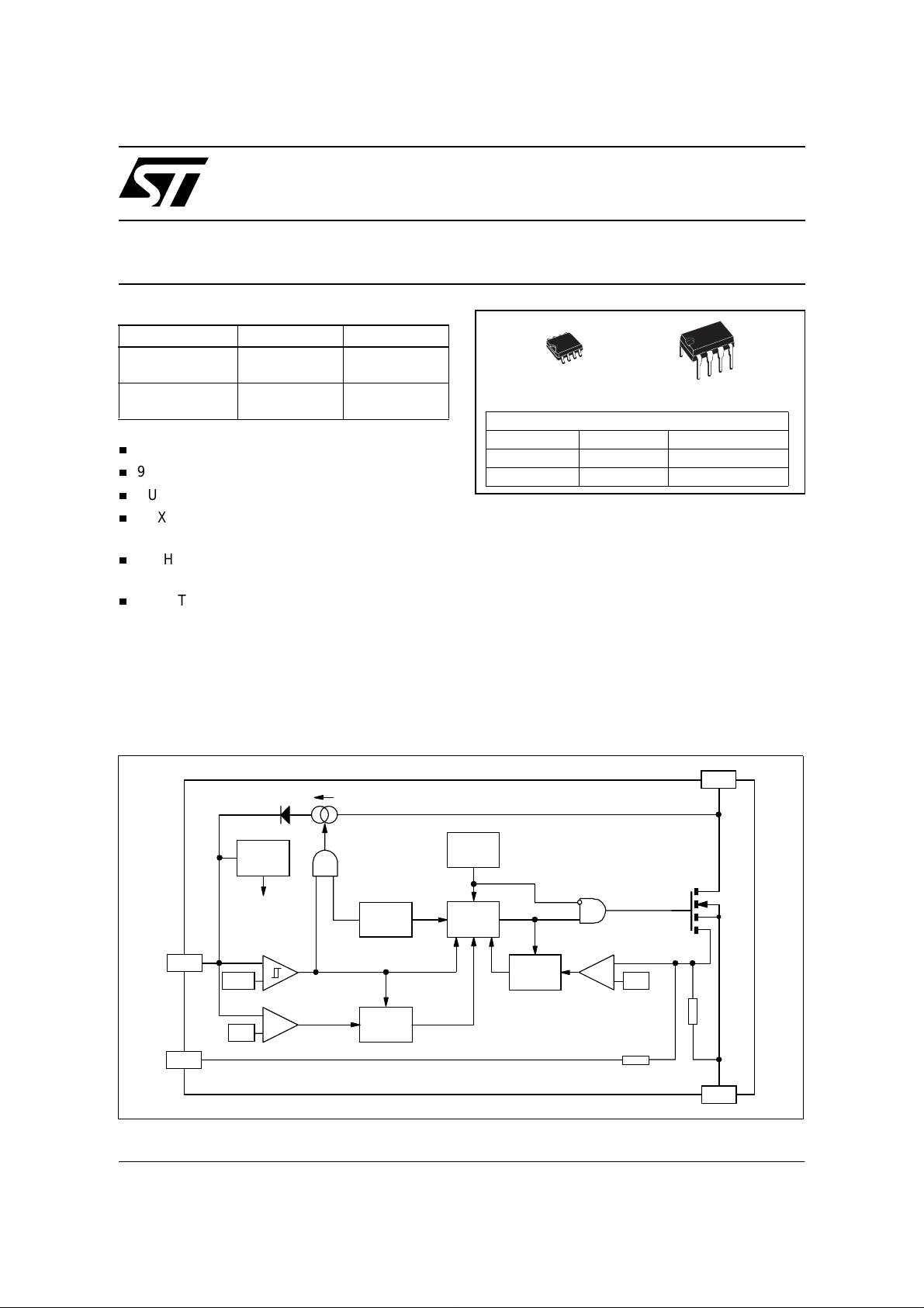
VIPer12ADI P
®
LOW POWER OFF LINE SMPS PRIMARY SWITCHER
TYPICAL POWER CA PABILITY
Main s t y pe SO-8 DIP8
European
(195 - 265 Vac)
US / Wide range
(85 - 265 Vac)
n
FIXED 60 KHZ SWITCHING FREQUENCY
n
9V TO 38V WIDE RANGE V
n
CURRENT MODE CONTROL
n
AUXILIARY UNDERVOLTAGE LOCKOUT
WITH HYSTERESIS
n
HIGH VOLTAGE START UP CURRENT
SOURCE
n
O VERTEMPERATURE, OVE RCURRENT AND
OVERVOLTAGE PROTECTION WITH
AUTORESTAR T
DESCRIPTION
The VIPer12A combines a dedicated current mode
PWM controller with a high voltage Power
8 W 13 W
5 W 8 W
VOLTAGE
DD
VIPer12AS
SO-8 DIP-8
ORDER CODES
PACKAGE TUBE T&R
SO-8 VIPer12AS VIPer12AS13TR
DIP-8 VIPer12ADIP
MOSFET on the same silicon chip. Typical
applications cover off line power supplies for
battery charg er adapter s, stan dby pow er suppl ies
for TV or monitors, auxiliary supplies for motor
control, etc. The i nternal control circuit offers the
following benefits:
– Large input voltage range on the VDD pin
accommodates changes in auxiliary supply
voltage. This fe ature is well adapted to battery
charger adapter configurations.
– Automatic burst mode in low load condition.
– Overvoltage protection in hiccup mode.
BLO C K DIAGRA M
DRAIN
ON/OFF
REGULATOR
INTERNAL
VDD
FB
8/14.5V
42V
SUPPLY
_
+
+
_
OVERTEMP.
DETECTOR
R
FF
S
OVERVOLTAGE
Q
Septe m ber 2002 1/15
LATCH
60kHz
OSCILLATOR
S
FF
R1
R4QR3
R2
PWM
LATCH
BLANKING
+
_
0.23 V
230
Ω
1 k
Ω
SOURCE
Page 2
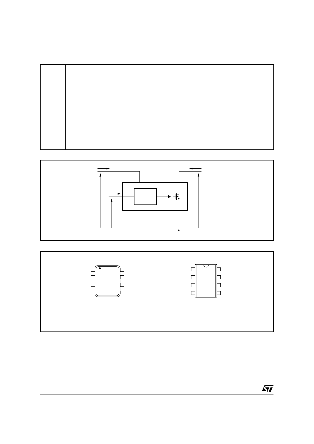
VIPer12ADIP / VIPer12AS
PIN FUNCTION
Name Function
Power supply of the control circuits. Also provides a charging current during start up thanks to a high
voltage current sour ce connected to the drai n. For this p urpose, an hysteresis comparator mo nitors the
voltage and provides two thres holds:
V
DD
V
SOURCE Power MOSFET source and circuit ground reference.
DRAIN
FB
CURRENT AND VOLTAGE CONVENTIONS
- V
DD
: Voltage value (typically 14.5V) at whi ch the device starts switching and tur ns off the start up
DDon
curre nt source.
- V
: Voltage value (typically 8V) at which the device stops switching and turns on the start up current
DDoff
source.
Power MOSFET drain. Al so used by the internal high voltage cu rrent source during start up phase for
charging the extern al V
capacitor.
DD
Feedbac k input. The useful voltage range extends from 0V to 1V, and defines the pea k drain MOSFET
current. The current limitation, which corresponds to the maximum drain current, is obtained for a FB pin
shorted to the SOURCE pin.
I
DD
I
D
V
DD
CONNECTION DIAGRAM
FB
VDD
1
2
3
4
SOURCE
SOURCE SOURCE
I
FB
V
FB
VDD DRAIN
FB
CONTROL
VIPer12A
8
DRAIN
7
DRAIN
6
DRAIN
5
DRAIN
SOURCE
SOURCE
FB
VDD
V
D
1
2
3
4
SO-8 DIP8
8
7
6
5
DRAIN
DRAIN
DRAIN
DRAIN
2/15
Page 3

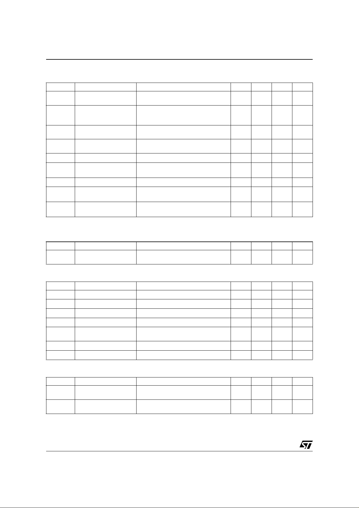
VIPer12ADIP / VIPer12AS
ABSOLUTE MAXIMUM RATI NGS
Symbol Parameter Value Unit
V
DS(sw)
V
DS(st)
I
V
I
FB
V
ESD
T
T
T
Note: 1. This parameter applies when the start up current source is off. This is the case when the VDD voltage has reached V
THERMAL DATA
Symbol Parameter Max Value Unit
Rthj-case
Rthj-amb
Note: 1. When mounted on a standard single-sided FR4 board with 200 mm² of Cu (at least 35 µm thick) connected to all DRAIN pins.
Switchin g Drain Source Voltage (Tj=25 ... 125 ° C) (See note 1)
Start Up Drain Source Voltage (Tj=25 ... 12 5°C) (See note 2)
Continuous Drain Current Internally limited A
D
Supply V o ltage 0 ... 50 V
DD
-0.3 ... 730 V
-0.3 ... 400 V
Feedbac k Current 3 mA
Electrostatic Discharge:
Machine Model (R=0Ω; C=200pF)
Charged Device Model
Junction Operating Temperature Internally limited °C
j
Case Oper ating Temperature -40 to 150 °C
c
Storage Temperature -55 to 150 °C
stg
remains ab ov e V
2. This parameter applies when the s tart up current source is on. This is the case when the V
or has fallen below V
DDoff
.
DDoff
.
DD
200
1.5
voltage has not yet reached V
Thermal Resistance Junction-P ins for:
SO-8
DIP8
25
15
Thermal Resistance Junction-A m bient for:
SO-8 (See note 1)
DIP8 (See note 1)
55
45
kV
DDon
°C/W
°C/W
V
and
DDon
ELECTRICAL CHARACTERISTICS (Tj=25°C, VDD=18V, unless otherwise specified)
POWER SECTION
Symbol Parameter Test Conditions Min. Typ. Max. Unit
BV
I
DSS
R
DSon
C
Note: 1. On clamped inductiv e load
Drain-Source Voltage
DSS
Off State Drain Current
Static Drain-Source
On State Resistance
t
Fall Time
f
t
Rise Time
r
Drain Capaci tance
oss
I
=1mA; VFB=2V
D
V
=500V; VFB=2V; Tj=125°C
DS
=0.2A
I
D
I
=0.2A; Tj=100°C
D
=0.1A; VIN=300V (See fig.1)
I
D
(See note 1)
=0.2A; VIN=300V (See fig.1)
I
D
(See note 1)
V
=25V
DS
730 V
0.1 mA
27 30
54
100 ns
50 ns
40 pF
Ω
3/15
Page 4
VIPer12ADIP / VIPer12AS
ELECTRICAL CHARACTERISTICS (Tj=25°C, VDD=18V, unless otherwise specified)
SUPPLY SECTION
Symbol Parameter Test Conditions Min. Typ. Max. Unit
I
DDch
I
DDoff
I
DD0
I
DD1
D
RST
V
DDoff
V
DDon
V
DDhyst
V
DDovp
Note: 1. These test condit ions obtained with a resist iv e load are lead ing to the maxim um c onduction time of the device.
S ta r t Up Ch arging
Current
S ta r t Up Ch arging
Current
in Thermal Shutdown
Oper ating Supply Current
Not Switching
Oper ating Supply Current
Switching
DS=100V; V
V
=5V; VDS=100V
V
DD
> TSD - T
T
j
=2mA
I
FB
I
=0.5mA; ID=50mA (Note 1)
FB
DD
HYST
=5V ...V
(See fig. 2)
DDon
-1 mA
0mA
35mA
4.5 mA
Restart Duty Cycle (See fig. 3) 16 %
V
Undervoltage
DD
Shut do w n Th reshold
VDD Start Up Threshold
VDD Threshold
Hysteresis
VDD Overvo ltage
Threshold
(See fig. 2 & 3) 7 8 9 V
(See fig. 2 & 3) 13 14.5 16 V
(See fig. 2) 5.8 6.5 7.2 V
38 42 46 V
OSCILLATOR SECTION
Symbol Parameter Test Conditions Min. Typ. Max. Unit
F
OSC
Oscillator Frequency
Total Variation
V
DD=VDDoff
... 35V; Tj=0 ... 100°C
54 60 66 kHz
PWM COMPARATOR SECTION
Symbol Parameter Test Conditions Min. Typ. Max. Unit
G
I
Dlim
I
FBsd
R
t
t
t
ONmin
IFB to ID Current Gain
ID
V
Peak Current Limitation
=0V (See fig. 4)
FB
IFB Shutdown Cur rent
I
FB Pin Input Impedance
FB
Current Sense Delay to
d
Turn-Off
Blanking Time 500 ns
b
=0mA (See fig. 4)
D
I
=0.2A
D
(See fig. 4) 320
0.32 0.4 0.48 A
(See fig. 4) 0.9 mA
1.2 kΩ
200 ns
Minimum Turn On Time 700 ns
OVERTEMPERATURE SECTION
Symbol Parameter Test Conditions Min. Typ. Max. Unit
Thermal Shutdown
SD
Temperature
Thermal Shutdown
Hysteresis
(See fig. 5) 140 170 °C
(See fig. 5) 40 °C
T
T
HYST
4/15
Page 5
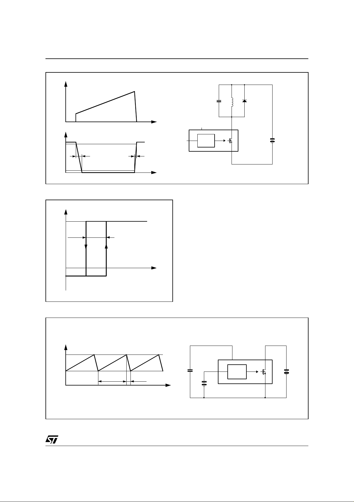
Figur e 1 : Rise and Fall Time
I
D
V
DS
90%
t
fv
VIPer12ADIP / VIPer12AS
L D
C << Coss
t
VDD DRAIN
FB
CONTROL
t
rv
VIPer12A
C
300V
SOURCE
10%
Figur e 2 : Start Up VDD Current
I
DD
I
DD0
V
DDhyst
I
DDch
V
DDoff
V
DDon
VDS = 100 V
F
sw
Figur e 3 : Restart Duty Cycle
= 0 kHz
t
V
DD
V
V
V
DDon
DDoff
DD
D
RST
VDD DRAIN
10µF
t
CH
-------------------------=
tSTtCH+
t
ST
t
ST
t
FB
CONTROL
2V
VIPer12A
SOURCE
100V
5/15
Page 6

VIPer12ADIP / VIPer12AS
Figur e 4 : Peak Drain Current Vs. Feedback Current
I
D
I
Dpeak
1/F
OSC
I
FBsdRFB
The drain current limitation is
obtained for VFB = 0 V, and a
negative current is drawn from
the FB pin. See the Application
section for further details.
t
V
FB
⋅
I
Dpeak
I
Dlim
18V
G
ID
I
FB
I
∆
---------------------- -–=
∆
47nF
Dpeak
I
FB
VDD DRAIN
FB
CONTROL
VIPer12A
I
FB
100V
4mH
100V
SOURCE
Figur e 5 : Thermal Shutdown
T
j
T
V
V
DDon
SD
DD
T
HYST
Automatic
start up
I
FB
0
I
FBsd
t
t
6/15
Page 7

Figur e 6 : Switching Frequency vs Tempera ture
1.01
1
0.99
Normalized Frequency
0.98
0.97
-20 0 20 40 60 80 100 120
VIPer12ADIP / VIPer12AS
Vdd = 10V ... 35V
Temperature (°C)
Figur e 7 : Current Limitation vs Temperature
1.04
1.03
1.02
1.01
1
0.99
0.98
0.97
0.96
Normalized Current Limitation
0.95
0.94
-20 0 20 40 60 80 100 120
Vin = 100V
Vdd = 20V
Temperature (°C)
7/15
Page 8

VIPer12ADIP / VIPer12AS
Figur e 8 : Rectangular U-I output characteristics for battery charger
AC IN
R1
C2
D1
F1
T2
C3
D4
C4
-+
ISO1
C5
C10
U1
FB
C6
VIPerX2A
R7R5R8
R10
D3
VDD DRAIN
CONTRO L
SOURCE
R2
U2
R3
C8
TSM101
Vcc
Vref
-
+
GND
T1
C7
D5
+
-
C1
D2
R4
C9
DCOUT
R6
R9
GND
RECTANGULAR U-I OUTPUT
CHARACTERISTIC
A complete regulation scheme can achieve
combined and accurate output characteristics.
Figure 8 prese nts a secondar y feedback thro ugh
an optocoupl er driven by a TSM101. This dev ice
offers two operational amplifiers and a voltage
reference, thus allowing the regulation of both
output voltage and current. An integrated OR
function performs the combination of the two
resulting error signals, leading to a dual voltage
and current limitation, known as a rectangular
output characteri stic .
This type of pow er supply is especial ly useful for
battery chargers where the output is mainly used in
current mode, in order to deliver a defined charging
rate. The accurate voltage regulation is also
convenien t for Li-ion batterie s which require both
modes of operation.
8/15
WIDE RANGE OF VDD VOLTAGE
The VDD pin voltage range extends from 9V to 38V.
This feature offers a great flexibility in design to
achieve various behaviors. In figure 8 a forward
configuration has been chosen to supply the
device with two benefits:
– as soon as the device starts switching, it
immediately receives some energy from the
auxiliary winding. C5 can be therefore reduced
and a small ceramic chip (100 nF) is sufficient to
insure the filtering function. The total start up
time from the switch on of input voltage to output
voltage presence is dramatically decreased.
– the output current characteristic can be
maintained even with very low or zero output
voltage. Since the TSM101 is also supplied in
forward mode, it keeps the current regulation up
whatever the output voltage is.The VDD pin
voltage may vary as m uch a s the input voltag e,
that is to say with a ratio of about 4 for a wide
range application.
Page 9

VIPer12ADIP / VIPer12AS
Fi
R2ISIFB+()⋅ 0.23V=
I
S
0.23V
R
2
-------------- IFB–=
I
FB
0.23V
R
1
--------------–=
Fi
I
FEEDBACK PIN PRINCIPLE OF OPERATION
A feedback pin controls the operation of the
device. Unli ke conventional PWM control circuits
which use a voltage input (the inverted inp ut of an
operational amplifier), the FB pin is sensitive to
current. Figure 9 presents the internal current
mode structure.
The Power MOS FET delivers a sense current I
which is proportional to the main current Id. R2
receives this cu rrent and the current coming from
the FB pin. The voltage across R2 is then
compared to a fixed reference voltage of about
0.23 V. The MOSFET is switched off when the
following equation is reached:
By extracting IS:
Using the current sense ratio of the MOSFET GID:
0.23V
I
D
GIDIS⋅ G
-------------- IFB–
⋅==
ID
R
2
The curren t limitation is obt ained with the FB pin
shorted to ground (VFB = 0 V). This leads to a
negative current sourced by this pin, and
expressed by:
By reporting this expression in the previous one, it
is possible to obtain the drain current limitation
I
:
Dlim
I
Dlim
GID0.23V
⋅⋅=
1
------
R
1
----- -+
R
2
1
gure 9 : Internal Current Control Structure
60kHz
OSCILLATOR
Secondary
feedback
+Vdd
I
FB
FB
C
0.23V
1 kΩ
S
PWM
Q
LATCH
R
R1
R2
230 Ω
DRAIN
Is
SOURCE
In a real applicat ion, the FB pin is driven w ith an
optocoupler as sho w n o n figu re 9 wh ich act s as a
pull up. So, it is not possible to really short this pin
to ground and the above drain current value is not
achievable. Nevertheless, the capacitor C is
averaging the voltage on the FB pin, and when the
optocoupler is off (start up or short circuit), it can be
assumed that the corresponding voltage is very
s
close to 0 V.
For low dr ain curre nts, the form ula (1) is valid as
long as IFB satisfies IFB< I
internal threshol d of the VIPer12A. If IFB exceeds
FBsd
, where I
FBsd
is an
this threshold the d evice will sto p switchin g. T his is
represented on figure 4, and I
specified in the PWM COMPARATOR SECTION.
value is
FBsd
Actually, as soon as the drain current is about 12%
of Idlim, that is to say 50 mA, the device will enter
a burst mode operation by missing switching
cycles. This is especially important when the
converter is lightly loaded.
It is then possible to build the total DC transfer
function between ID and IFB as shown on figure 10.
This figure also takes into account the internal
blanking time and it s associated minimum tur n on
time. This imposes a minimum drain current under
which the device is no more able to control it in a
linear way. This drain current depends on the
primary inductance value of the transformer and
the input voltage. Two cases may occur,
depending on the val ue of this curr ent versus the
fixed 50 mA value, as described above.
START UP SEQUENCE
This device includes a high voltage start up current
source connecte d on the drain of the device. As
soon as a voltage is applied on the input of the
converter, this start up cur rent source is activat ed
as long as VDD is lower than V
reaching V
switched off and the device begins to o perate by
Id
turning on and off its main power MOSFET. As the
FB pin does not receive any current from the
, the start up current source is
DDon
DDon
. When
optocoupler, the device operates at full current
capacity and the output voltage rises until reaching
gure 10 :
t
ONmin
---------------------------------------
L
t
ONmin
---------------------------------------
L
Transfer function
FB
I
Dpeak
I
Dlim
1
V
⋅
IN
50mA
2
V
⋅
IN
0
Part masked by the
I
threshold
FBsd
I
FBsd
I
FB
9/15
Page 10

VIPer12ADIP / VIPer12AS
Fi
Fi
gure 11 : Start Up Sequence
V
DD
V
DDon
V
DDoff
tss
t
I
FB
t
V
OUT
t
the regulation point where the secondary loop
begins to send a current in the optocoupler. At this
point, the converter ent ers a regulated operation
where the F B pin receives the amount of current
needed to deliver the right power on secondary
side.
This sequence is shown in figure 11. Note that
during the real starting phase tss, the device
consumes some energy from the VDD capacitor,
waiting for the auxiliary winding to provide a
continuous s upply. If th e value of this c apacitor i s
too low, th e start up phase is terminated before
receiving any energy from the auxiliary winding
and the converter never starts up. This is illustrated
also in the same figure in dashed lines.
gure 12 : Overvoltage Sequence
V
DD
V
DDovp
V
DDon
V
V
DDoff
DS
t
t
OVERVOLTAGE THRESHOLD
An overvoltage dete c tor on the VDD pin allows the
VIPer12A to reset itself when VDD exceeds
V
. This is illustrated in figure 12, which shows
DDovp
the whole sequence of an overvoltage event. Note
that this event i s only latche d for the time needed
by VDD to reach V
resumes normal operati on autom atic ally .
, and then the device
DDoff
10/15
Page 11

SO-8 MECHANICAL DATA
VIPer12ADIP / VIPer12AS
DIM.
A 1.75 0.068
a1 0.1 0.25 0.003 0.009
a2 1.65 0.064
a3 0.65 0.85 0.025 0.033
b 0.35 0.48 0.013 0.018
b1 0.19 0.25 0.007 0.010
C 0.25 0.5 0.010 0.019
c1 45 (typ .)
D 4 .8 5 0.188 0.196
E
e 1.27 0.050
e3 3.81 0.150
F 3.8 4 0.14 0.157
L 0.4 1.27 0.015 0.050
M 0.6 0.023
S 8 (max.)
L1 0.8 1.2 0.031 0.047
MIN. TYP MAX. MIN. TYP. MAX.
5.8
mm. inch
6.2 0.228 0.244
11/15
1
Page 12

VIPer12ADIP / VIPer12AS
Plastic DIP-8 MECHANI CAL DATA
DIM.
A 5.33
A1 0.38
A2 2.92 3.30 4.95
b 0.36 0.46 0.56
b2 1.14 1.52 1.78
c 0.20 0.25 0.36
D 9.02 9.27 10.16
E 7.62 7.87 8.26
E1 6.10 6.35 7.11
e2.54
eA 7.62
eB 10.92
L 2.92 3.30 3.81
Packag e W eight Gr. 470
MIN. TYP MAX.
mm.
12/15
P001
Page 13

SO-8 TUBE SHIPMENT (no suffix)
VIPer12ADIP / VIPer12AS
B
C
Base Q.ty 100
Bulk Q.ty 2000
Tube length (± 0.5) 532
A
A 3.2
B 6
C (± 0.1) 0.6
All dimensions are i n m m .
TAPE AND REEL SHIPMENT (suffix “13TR”)
REEL DIMENSIONS
Base Q.ty 2500
Bulk Q.ty 2500
A (max) 330
B (min) 1.5
C (± 0.2) 13
F 20.2
G (+ 2 / -0) 12.4
N (min) 60
T (max) 18.4
All dimensions are i n m m .
TAPE DIMENSIONS
According to Electronic Industries Asso ciation
(EIA) S tanda rd 481 re v. A, Feb 1 9 86
Tape width W 12
Tape Hole Spacing P0 (± 0.1) 4
Component Spacing P 8
Hole Diameter D (± 0.1/-0) 1.5
Hole Diameter D1 (min) 1.5
Hole Position F (± 0.05) 5.5
Compartment Depth K (max) 4.5
Hole Spacing P1 (± 0.1) 2
All dimensions are i n m m .
Top
cover
tape
End
500mm min
Empty components pockets
saled with cover tape.
User direction of feed
Start
No componentsNo components Components
500mm min
13/15
1
Page 14

VIPer12ADIP / VIPer12AS
DIP-8 TUBE SHIPMENT (no suffix)
A
C
Base Q.ty 20
Bulk Q.ty 1000
Tube length (± 0.5) 532
A 8.4
B
B 11.2
C (± 0.1) 0.8
All dimensions are in mm.
14/15
11
Page 15

VIPer12ADIP / VIPer12AS
Information furnish ed is believed to be accurate and reliable. However, STMic r oelectroni c s as s um es no respons ibility for the cons equences
of use of such information nor for any infringement of patents or other rights of third parties which may results from its use. No license is
granted by implication or otherwise unde r any patent or pat ent rights of STMicroelectronics. Spe c ifications m entioned in thi s publication are
subject to c hange without notice. This public ation supers edes and replaces all information previously s upplied. STMicroel ec tronics pr oducts
are not authorized for use as critical components in life support devices or systems without express written approval of STMicroelectronics.
Australia - Brazil - Canada - Ch ina - Finland - Fr anc e - Germany - Ho ng K ong - India - Israel - Italy - J apan - Malaysia -
Malta - Morocco - Singapore - Spain - Sweden - Switzerland - United Kingdom - U.S.A.
The ST logo is a trademark of STMicroelectronics
2002 STMicroelectronics - Printed in ITALY- All Rights Reserved.
STMicroelectronics GROUP OF COMPANIES
http://www.st.com
15/15
 Loading...