

Page 1

VIPer100/SP
VIPer100A/ASP
SMPS PRIMARY I.C.
Table 1. General Features
Type
V
DSS
I
n
VIPer100/SP 620V 3 A
VIPer100A/ASP 700V 3 A
■ ADJUSTABLE SWITCHING FREQUENCY UP
R
DS(on)
2.5
2.8
Ω
Ω
TO 200 kHz
■ CURRENT MODE CONTROL
■ SOFT START AND SHUTDOWN CONTROL
■ AUTOMATIC BURST MODE OPERATION IN
STAND-BY CONDI T ION ABLE TO MEET
“BLUE ANGEL” NORM (<1w TOTAL POWER
CONSUMPTION)
■ INTERNALLY TRIMMED ZENER
REFERENCE
■ UNDERVOLTAGE LOCK-OUT WITH
HYSTERESIS
■ INTEGRATED START-UP SUPPLY
■ OVER-TEMPERATURE PROTECTION
■ LOW STAND-BY CURRENT
■ ADJUSTABLE CURRENT LIMITATION
Figure 1. Block Diagram
Figure 2. Package
PENTAWATT HV
PENTAWATT HV (022Y)
DESCRIPTION
VIPer100™/100A, made using VIPower M0
Technology, combines on the same silicon chip a
state-of-the-art PWM circuit together with an
optimized, high voltage, Vertical Power MOSFET
(620V or 700V / 3A).
Typical applications cover offline power supplies
with a secondary power capability of 50 W in wide
range condition and 100W in single range or with
doubler configuration. It is compatible from both
primary or secondary regulation loop despite
using around 50% less components when
compared with a discrete solution. Burst mode
operation is an additional feature of this device,
offering the ability to operate in stand-by mode
without extra components.
_
1 V/A
CURRENT
AMPLIFIER
DRAIN
SOURCE
1
3
2
0
0
C
F
OSC
ON/OFF
SECURITY
LATCH
ERROR
AMPLIFIER_
UVLO
LOGIC
0.5 V +
V
DD
13 V
+
_
4.5 V
R/S
OVERTEMP.
DETECTOR
1.7
DELAY
FF
QSR1
S
s
μ
OSCILLATOR
PWM
LATCH
FF
R2 R3
COMP
Q
250 ns
BLANKING
0.5V
+
+
_
Rev 2
June 2005 1/24
www.st.com
24
Page 2
VIPer 100/SP - VIPe r100A/A SP
I
I
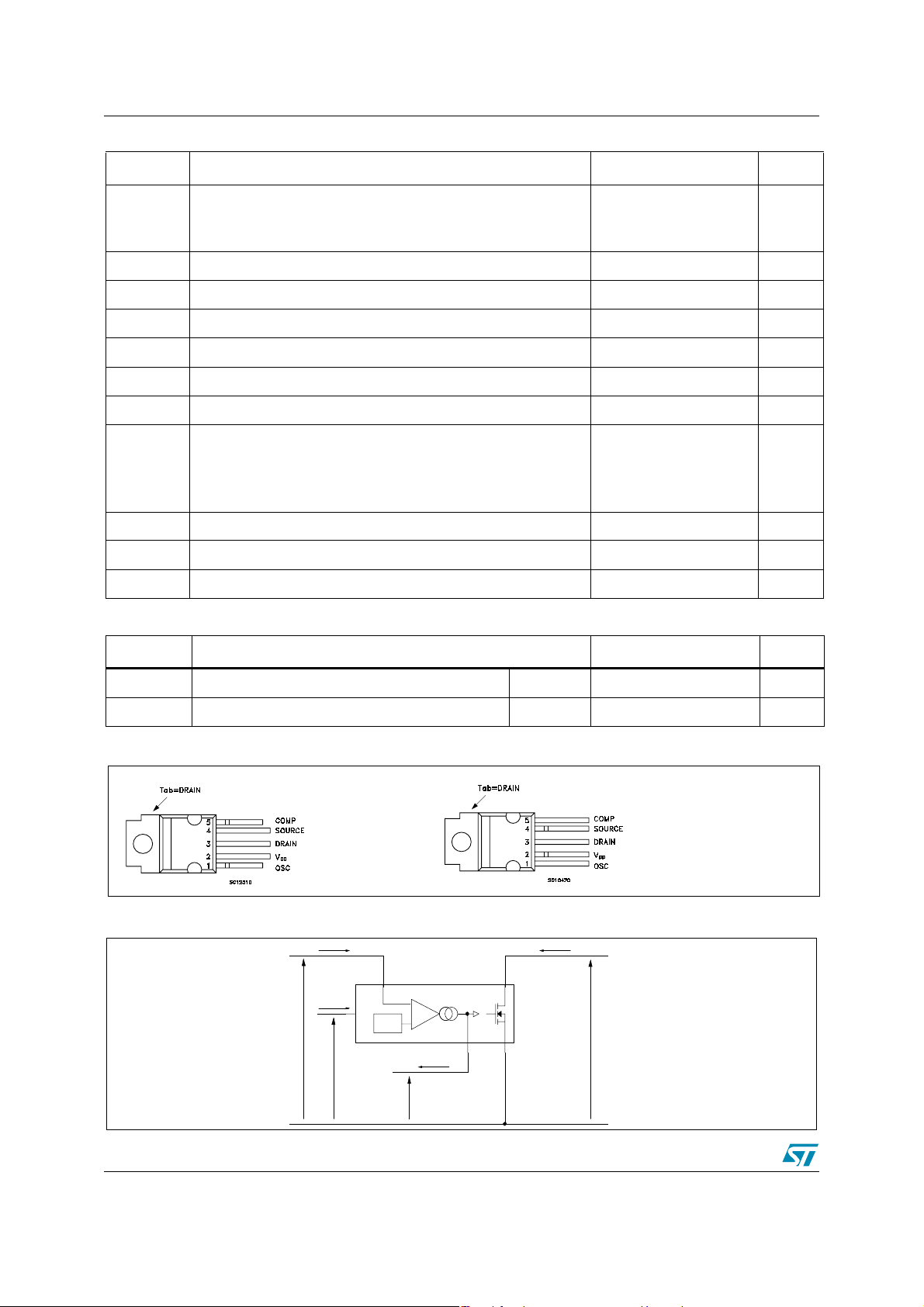
Table 2. Absolute Maximum Rating
Symbol Parameter Value Unit
Continuous Drain-Source Vol tage (TJ = 25 to 125°C)
V
V
V
OSC
V
COMP
I
COMP
V
ESD
I
DS
D
DD
for VIPer100/SP
for VIPer100A/ASP
–0.3 to 620
–0.3 to 700
Maximum Current Internally lim ited A
Supply Voltage 0 to 15 V
Voltage Range Input
0 to V
DD
Voltage Range Inpu 0 to 5 V
Maximum Continuous Curre nt ±2 mA
Electrostati c Discharge (R =1.5kΩ; C=100pF) 4000 V
Avalanche Drain-Source Current, Repetitive or Not Repetitive
I
D(AR)
P
tot
T
T
stg
(Tc=100°C; Pulse width limit ed by TJ m ax; δ < 1%)
for VIPer100/SP
for VIPer100A/ASP
Power Dissipation at Tc=25ºC
Junction Operating Temperature Internally lim ited °C
j
2
1.4
82 W
Storage Temperature -65 to 150 °C
Table 3. Thermal data
Symbol Parameter PENTAWATT HV Unit
V
V
V
A
A
R
thj-case
R
thj-amb
Thermal Resistance Junction-case Max 1.4 °C/W
Thermal Resistance Ambient-case Max 60 °C/W
Figure 3. Connection Diagrams (Top View)
PENTAWATT HV
PENTAWATT HV (022Y)
Table 4. Current and Voltage Convention
DD
I
OSC
OSC
V
DD
V
OSC
13V
+
I
COMP
V
COMP
DRAINVDD
COMP SOURCE
D
V
DS
2/24
Page 3

VIPer100/SP - VIPer100A/ASP
Table 5. Ordering Numbers
PENT AWATT HV PENTAWATT HV (022Y)
VIPer100
VIPer100A
VIPer100 (022Y)
VIPer100A (022Y)
Pins Functional Description
Drain Pin (Integrated Power MOSFET Drain):
Integrated Power MOSFET drain pin. It provides internal bias current during start-up via an integrated
high voltage current source which is switched off during normal operation. The device is able to handle
an unclamped current during its normal operation, assuring sel f protection aga inst voltage s urges, PCB
stray inductance, and allowing a snubberless operation for low output power.
Suorce Pin:
Power MOSFET source pin. Primary side circuit common ground connection.
VDD Pin (Power Supply):
This pin provides two functions :
■ It corresponds to the low voltage supply of the control part of the circuit. If V
up current source is activated and the output power MOSFET is switched off until the V
reaches 11V. During this phase, the internal current consumption is reduced, the V
a current of about 2mA and the COMP pin is shorted to ground. After that, the current source is shut
down, and the device tries to start up by switching again.
■ This pin is also connected to the error amplifier, in order to allow primary as well as secondary
regulation configurations. In case of primary regulation, an internal 13V trimmed reference voltage is
used to maintain V
on V
pin by transformer design, in order to stuck the output of the transconductance amplifier to the
DD
at 13V. For secondary regulation, a voltage between 8.5V and 12.5V will be put
DD
high state. The COMP pin behaves as a constant current source, and can easily be connected to the
output of an optocoupler. Note that any overvoltage due to regulation loop failure is still detected by the
error amplifier through the V
voltage, which cannot overpass 13V. The output voltage will be
DD
somewhat higher than the nominal one, but still under control.
goes below 8V, the start-
DD
voltage
DD
pin is sourcing
DD
Compensation Pin
This pin provides two functions :
■ It is the output of the error transconductance amplifier, and allows for the connection of a compensation
network to provide the desired transfer function of the regulation loop. Its bandwidth can be easily
adjusted to the needed value with usual components value. As stated above, second ary regulation
configurations are also implemented through the COMP pin.
■ When the COMP voltage is going below 0.5V, the shut-down of the circuit occurs, with a zero duty cycle
for the power MOSFET. This feature can be used to switch off the converter, and is automatically
activated by the regulation loop (no matter what the configuration is) to provide a burst mode operation
in case of negligible output power or open load condition.
OSC Pin (Oscillator Frequency):
An Rt-Ct network must be connected on that to define the switching frequency. Note that despite the
connection of R
provides also a synchronisation capabilit y, when connected to an external frequency source.
to VDD, no significant frequency change occurs for VDD varying from 8V to 15V. It
t
3/24
Page 4
VIPer 100/SP - VIPe r100A/A SP
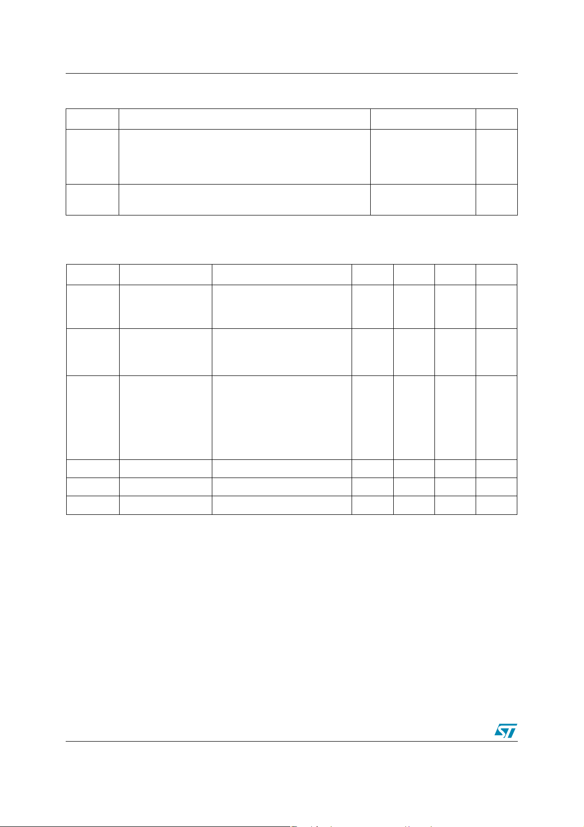
Table 6. Avalance Characteristics
Symbol Parameter Max Value Unit
Avalanche Curre nt, Re petitive or Not Repetitive
I
D(AR)
E
(AR)
(pulse width limited by TJ max; δ < 1%)
for VIPer100/SP (see Figu re 15)
for VIPer100A/ASP (*) (see Figure 15)
Single Pulse Avalanche Energy
= I
(starting TJ = 25ºC, I
D
D(ar)
) (*)
2
1.4
60 mJ
A
A
Electrical Chracteristics (TJ = 25°C; VDD = 13V, unless otherwise spec if ied)
Table 7. Power Section
Symbol Parameter Test Conditions Min Typ Max Unit
I
BV
I
DSS
R
DS(on)
C
t
f
t
r
oss
Drain-Source Voltage
DS
Off-State Drain
Current
St atic Drain-Source
On Resistance
Fall Ti me
Rise Time
Output Capacitance
= 1mA; V
D
for VIPer100/SP
for VIPer100A/ASP (see Figure 8)
V
= 0V; Tj = 125°C
COMP
= 620V for VIPer100/SP
V
DS
= 700V for VIPer100A/ASP
V
DS
= 2A
I
D
for VIPer100/SP
for VIPer100A/ASP
= 2A; Tj = 100°C
I
D
for VIPer100/SP
for VIPer100A/ASP
= 0.2A; V
I
D
= 0.4A; V
I
D
V
= 25V
DS
= 0V
COMP
=300V (1)Figure 6
IN
= 300V (1)Figure 6
IN
620
700
2.0
1
1
2.5
2.8
mA
mA
Ω
Ω
2.3
4.5
5.0
Ω
Ω
100 ns
50 ns
150 pF
V
V
(1) On Inductive Load, Clamped.
4/24
Page 5
VIPer100/SP - VIPer100A/ASP
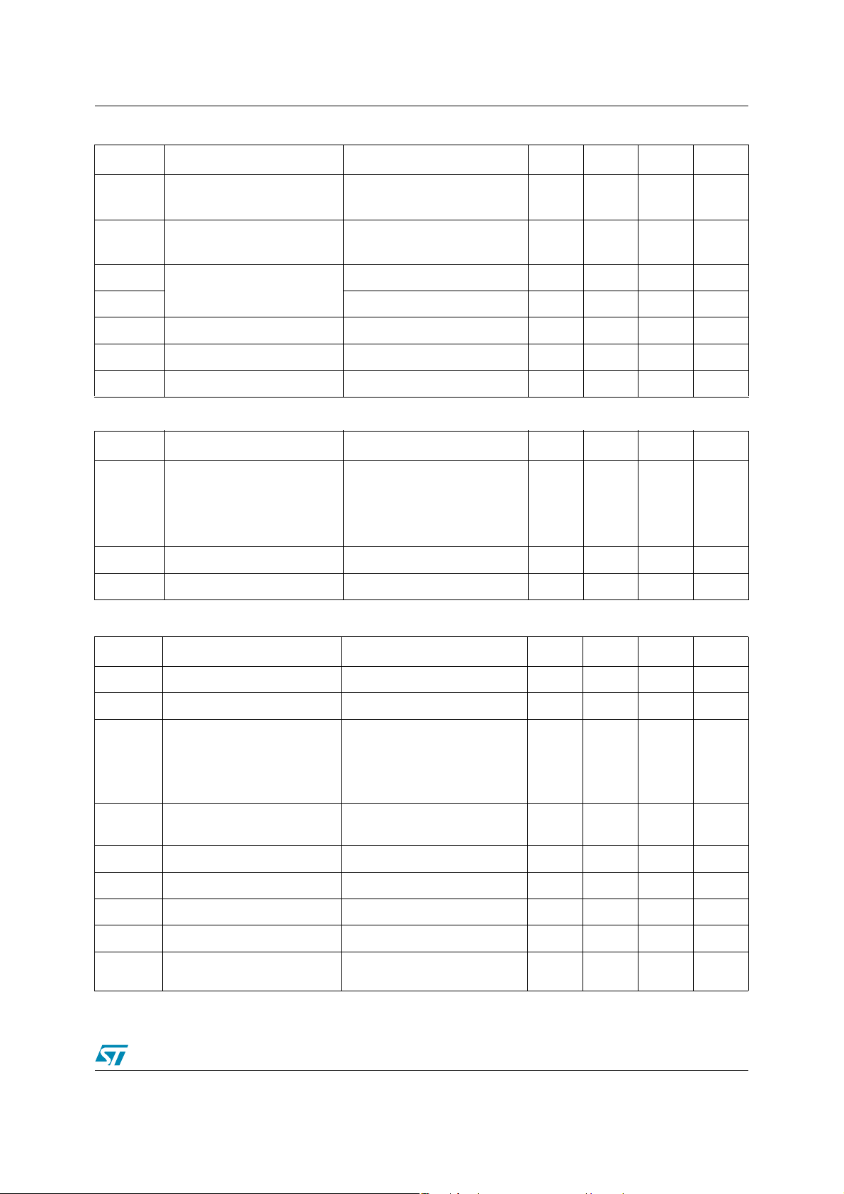
Table 8. Supply Section
Symbol Parameter Test Conditions‘ Min Typ Max Unit
= 5V; VDS = 35V
V
I
DDch
Start-Up Charging Current
DD
(see Figure 5)(see Fig ure 18)
-2 mA
I
DD0
I
DD1
V
DDoff
V
DDon
V
DDhyst
= 12V; F
V
Operating Supply Current
Operating Supply Current
DD
(see Figure 5)
= 12V; F
V
DD
V
= 12V; F
DD
Undervoltage Shutdown (see Figure 5) 7.5 8 9 V
Undervoltage Reset (see Figure 5) 11 12 V
Hysteresis Start-up (see Figure 5) 2.4 3 V
= 0kHz
SW
= 100kHz
sw
= 200kHz
sw
12 16 mA
15.5 mA
19 mA
Table 9. Oscillator Section
Symbol Parameter Test Conditions‘ Min Typ Max Unit
R
=8.2KΩ; CT=2.4nF
T
V
F
SW
Oscillator Frequency Total
Variation
=9 to 15V;
DD
with R
± 1%; CT± 5%
T
90 100 110 KHz
(see Figure 9)(see Fig ure 12)
V
OSCIH
V
OSCIL
Oscillator Peak Vol tage 7.1 V
Oscillator Valley Voltage 3.7 V
Table 10. Error Amplifier Section
Symbol Parameter Test Conditions‘ Min Typ Max Unit
V
DDREG
ΔV
DDreg
G
BW
VDD Regulation Point I
Total Variation
Unity Gain Bandwidth
=0mA (see Figure 4)
COMP
T
=0 to 100°C
j
From Input =V
Output = V
DD
COMP
COMP pin is open
12.6 13 13.4 V
2%
to
150 KHz
(see Figure 13)
A
VOL
G
m
V
COMPLO
V
COMPHI
I
COMPLO
I
COMPHI
Open Loop Voltage Gain
DC Transconductance
Output Low Level
Output High Level
Output Low Curre nt Capability
Output High Current
Capability
COMP pin is open
(see Figure 13)
V
=2.5V(see Figure 4)
COMP
=-400µA; VDD=14V
I
COMP
I
=400µA; VDD=12V
COMP
V
=2.5V; VDD=14V
COMP
V
=2.5V; VDD=12V
COMP
45 52 dB
1.1 1.5 1.9 mA/V
0.2 V
4.5 V
-600 µA
600 µA
5/24
Page 6
VIPer 100/SP - VIPe r100A/A SP
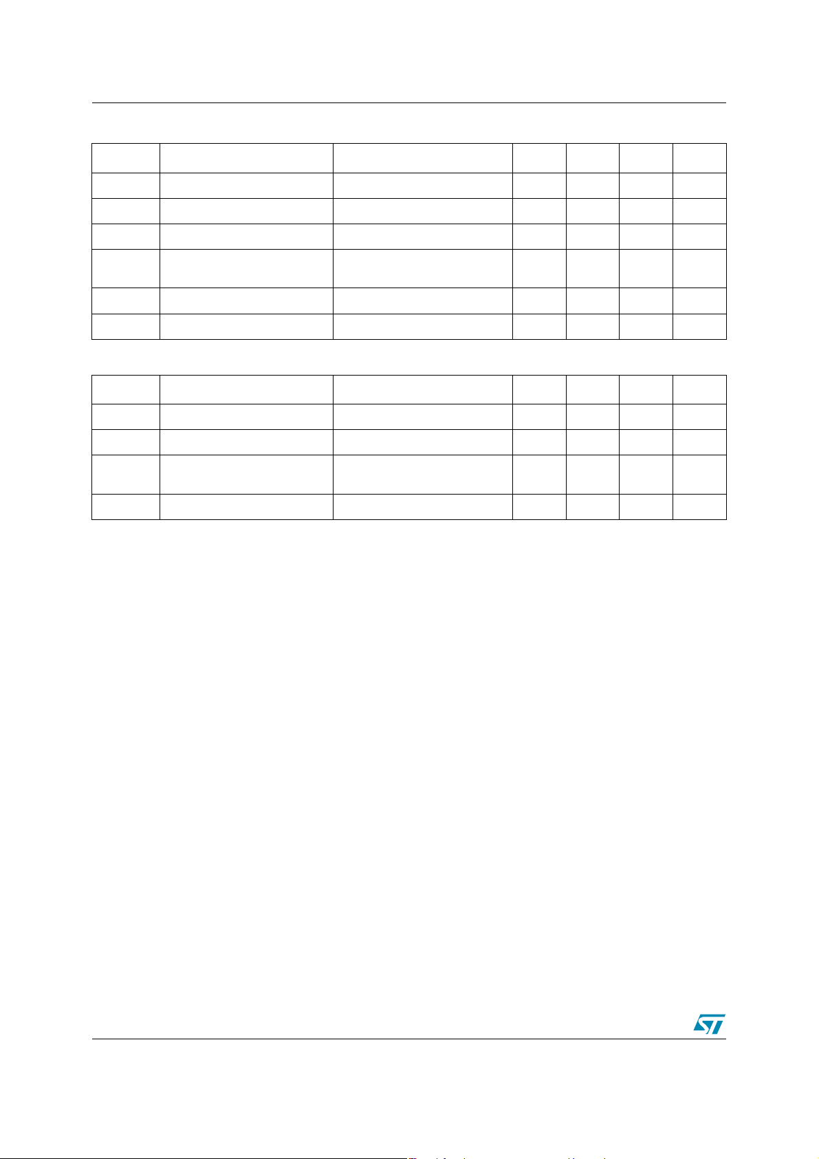
Table 11. PWM Comparator Section
Symbol Parameter Test Conditions‘ Min Typ Max Unit
H
V
COMPoffVCOMP
I
Dpeak
t
t
t
on(min)
ΔV
ID
Peak Current Limitat ion
Current Sense Delay to Turn-
d
Off
Blanking Ti m e 250 360 ns
b
/ ΔI
COMP
DPEAK
Offset I
V
= 1 to 3 V
COMP
= 10mA
DPEAK
V
= 12V; COMP pin open
DD
I
= 1A
D
0.7 1 1.3 V/A
0.5 V
345.3A
250 ns
Minimum On Time 350 1200 ns
Table 12. Shutdown and Overtemperature Section
Symbol Parameter Test Conditions‘ Min Typ Max Unit
V
COMPth
t
DISsu
T
T
hyst
Restart Threshold (see Figure 7) 0.5 V
Disable Set Up Time (see Figure 7) 1.7 5 µs
Thermal Shutdown
tsd
Temperature
(see Figure 7) 140 170 °C
Thermal Shutdown Hyst eresis (see Figure 7) 40 °C
6/24
Page 7
VIPer100/SP - VIPer100A/ASP
I
DD
I
D
V
V
0
(
140
(
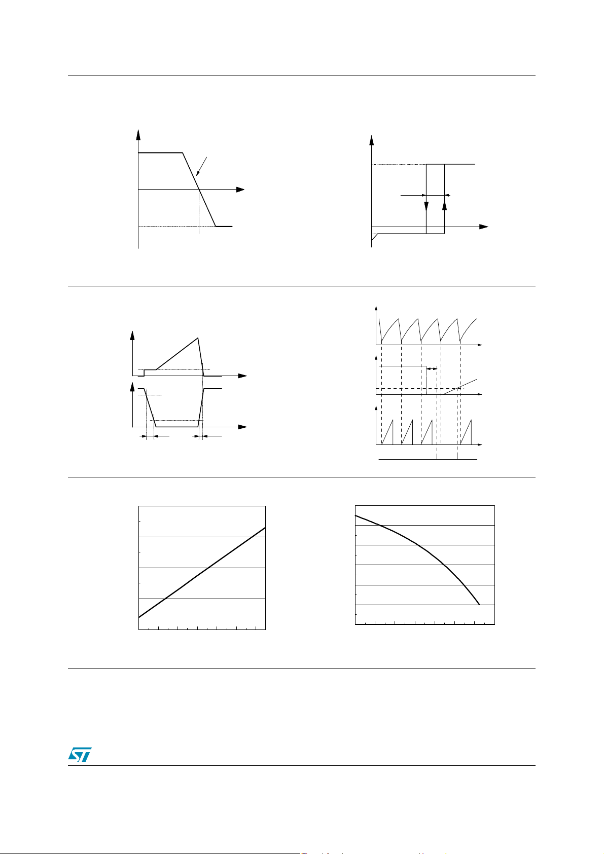
Figure 4. VDD Regulation P oint Figure 5. Undervoltage Loc kout
I
COM P
I
COMPHI
0
COMPLO
Figure 6. Trans i t ion Time Figure 7. Shutdown Action
Slope =
G m in mA/V
V
DDreg
FC00150
V
I
DD
DD0
I
DDch
VOSC
DDhyst
V
V
DDoff
VDS= 35 V
Fsw = 0
DDon
V
FC00170
V
D
ID
10% Ipeak
DS
90% V D
D
10% V
tf
t
t
tr
FC00160
VCOMP
COMPth
ID
tDISsu
ENABLE
DISABLE
t
t
t
ENABLE
FC0006
Figure 8. Breakdown Voltage vs. Temperature Figure 9. Typ ica l Freque ncy Variation
1.15
BVDSS
Normalized)
1.05
0.95
1.1
1
0 20406080100120
Temperature (°C)
FC00180
1
%)
0
-1
-2
-3
-4
-5
0 20 40 60 80 100 120
Temper at ure (°C)
FC00190
7/24
Page 8
VIPer 100/SP - VIPe r100A/A SP
T
T
t
t
t
t
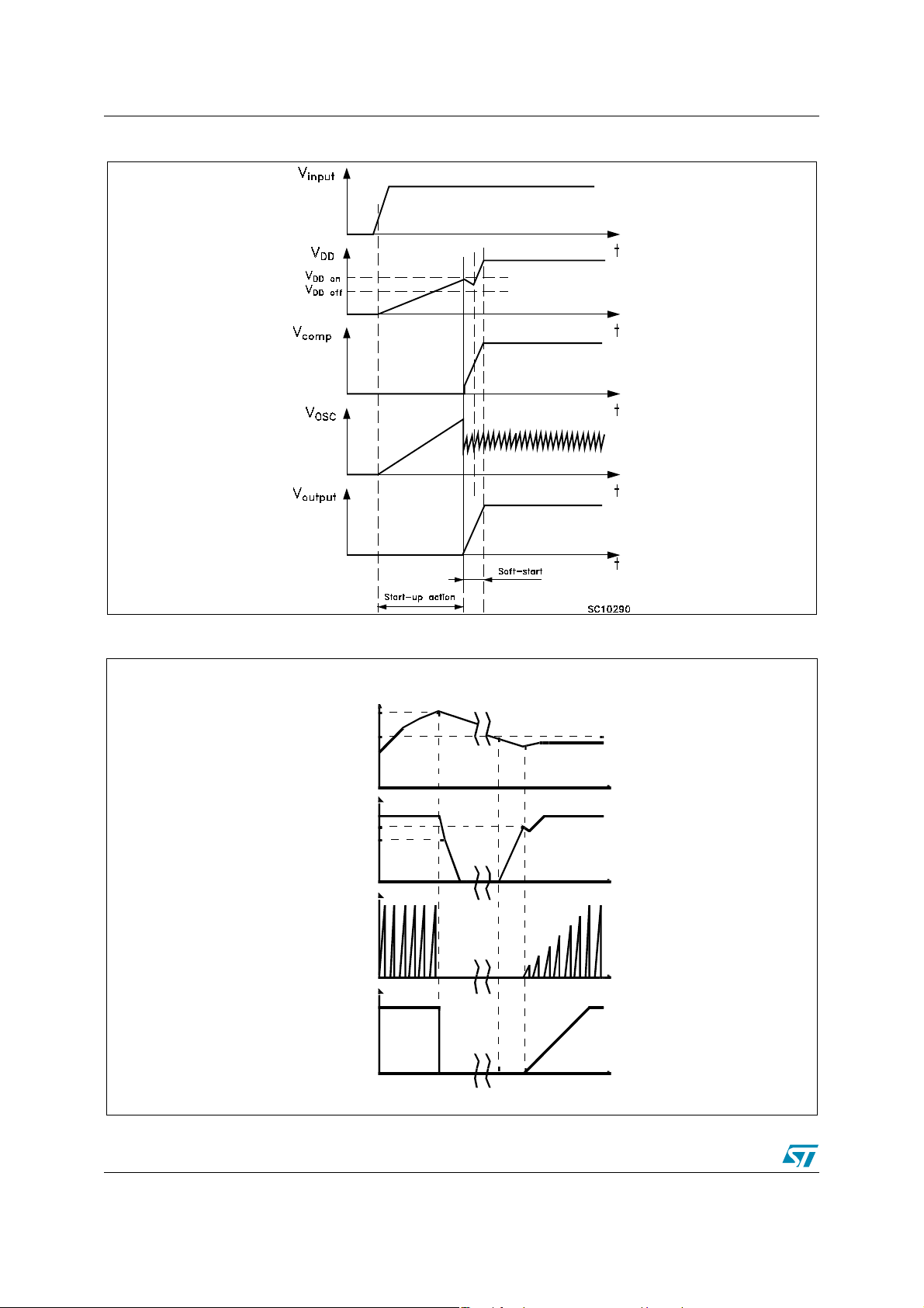
Figure 10. Start-Up Waveforms
Figure 11. Over-temperature Protection
J
T
ts c
tsd-Thyst
V
dd
V
ddon
V
ddoff
I
d
V
comp
SC101 91
8/24
Page 9
VIPer100/SP - VIPer100A/ASP
C
For Rt >1.2K
F
2.3
550
-
C
w
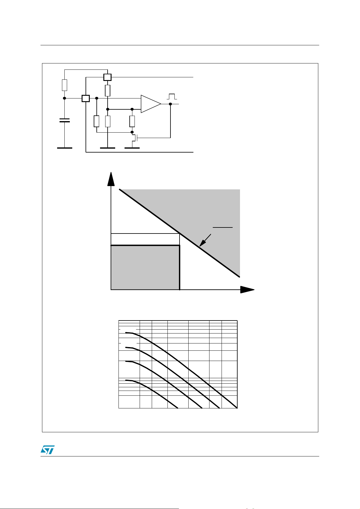
Figure 12. Oscillator
Rt
----------- 1
=
RtC
Ω
⎛⎞
–
---------------- ---
⋅
⎝⎠
Rt150–
t
VDD
OSC
CLK
t
Ω
and
C
≥ 15nF if FSW ≤ 40KHz
t
SW
~360
FC00050
t
Forbidden area
22nF
Ct(nF) =
15nF
880
Fsw(kHz)
1,000
500
300
200
100
Frequency (kHz)
Forbidden area
40kHz
Oscillator frequency vs Rt and Ct
FC00030FC00030
Ct = 1.5 nF
Ct = 2.7 nF
Ct = 4.7 nF
Ct = 10 nF
50
30
1 2 3 5 10 20 30 50
Rt (kΩ)
Fs
9/24
Page 10
VIPer 100/SP - VIPe r100A/A SP
0
0
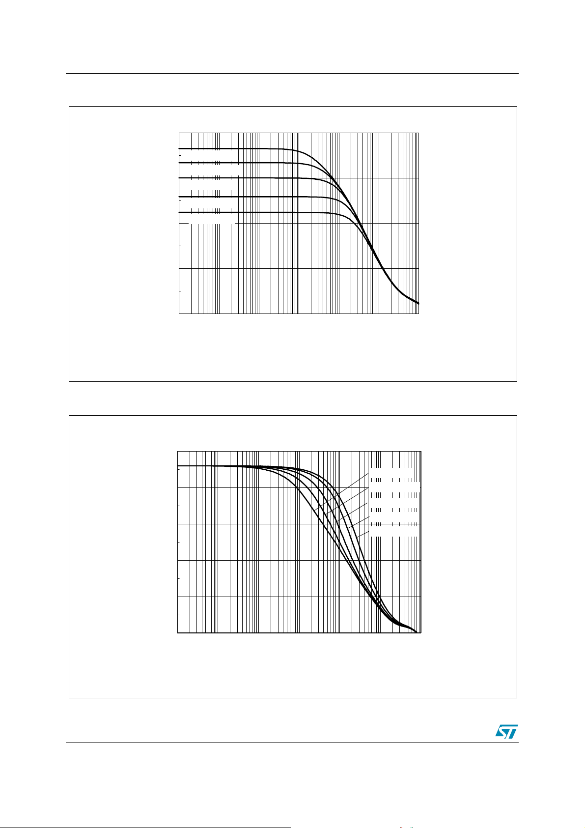
Figure 13. Error Amplifier frequency Response
FC00200
60
RCOMP = +
RCOMP = 270k
40
RCOMP = 82k
RCOMP = 27k
RCOMP = 12k
20
Voltage Gain (dB)
0
∞
(20)
0.001 0.01 0.1 1 10 100 1,00
Frequency (kHz)
Figure 14. Error Amplifier Phase Response
200
RCOMP = +
RCOMP = 270k
RCOMP = 82k
RCOMP = 27k
RCOMP = 12k
Phase (°)
150
100
50
0
(50)
0.001 0.01 0.1 1 10 100 1,00
Frequenc y ( k Hz )
FC00210
∞
10/24
Page 11
VIPer100/SP - VIPer100A/ASP
V
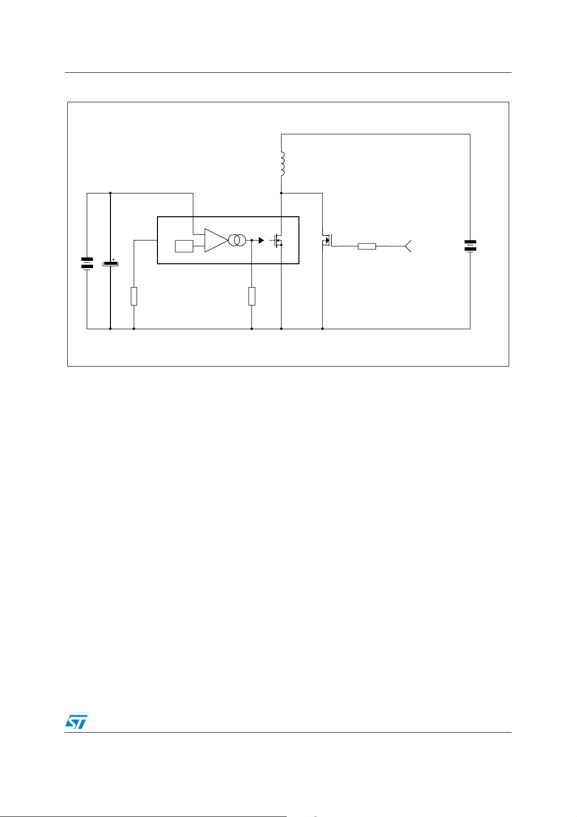
Figure 15. Avalanche Test Circuit
L1
1mH
BT2
12V
C1
47uF
16V
23
13V
-
+
COMP SOURCE
1
OSC
U1
VIPer100
R2
1k
DRAINVDD
54
R3
100
Q1
2 x STHV102FI in p arallel
R1
47
GENERATOR INPUT
500us PULSE
BT1
0 to 20
FC00195
11/24
Page 12
VIPer 100/SP - VIPe r100A/A SP
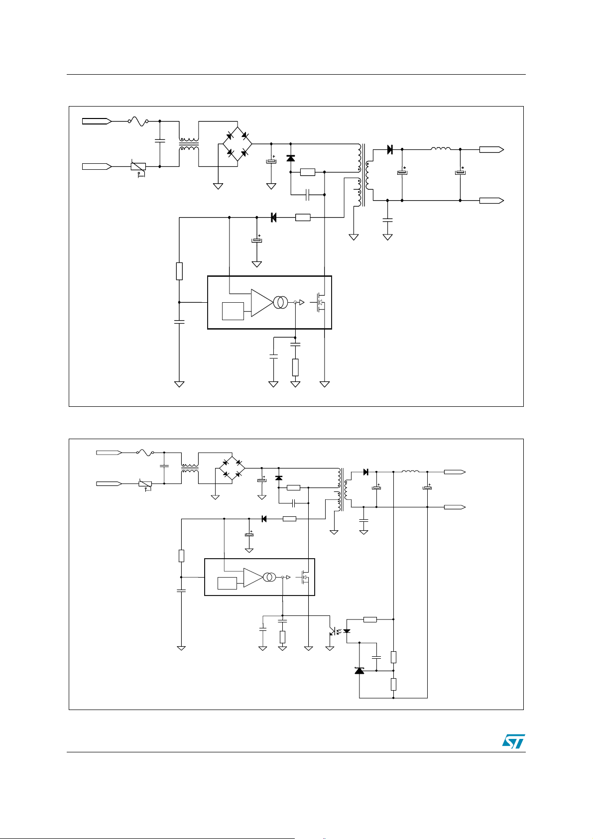
Figure 16. Offline Power Supply With Auxiliary Supply Feedback
F1
BR1
TR1
D2
D1
C2
R1
C7
L2
+Vcc
C9
AC IN
TR2
C1
R9
D3
C4
C3
R7
R2
DRAINVDD
13V
+
C11
COMP SOURCE
C6
OSC
C5
U1
VIPer100
R3
Figure 17. Offline Power Supply With Optocoupler Feedback
F1
BR1
TR1
D1
C2
C4
R1
D3
C3
R7
AC IN
TR2
C1
R9
GND
C10
FC00081
D2
C7
C10
L2
+Vcc
C9
GND
R2
13V
+
C11
OSC
C5
DRAINVDD
COMP SO URC E
C6
R3
12/24
U1
VIPer100
R6
ISO1
R4
U2
C8
R5
FC00091
Page 13

VIPer100/SP - VIPer100A/ASP
Operation Description:
Current Mode Topology :
The current mode control method, like the one integrated in the VIPer100/1 00A , uses two control loo ps an inner current con trol loop and an outer loop for voltage control. When the P ower MOSFET output
transistor is on, the inductor current (primary side of the transformer) is monitored with a SenseFET
technique and conv erted into a voltage V
amplified output voltage error) the power switch is switched off. Thus, the outer voltage control loop
defines the level at which the inner loop regulates peak current through the power switch and the primary
winding of the transformer.
Excellent open loop D.C. and dynamic line regulation is ensured due to the inherent input voltage
feedforward characteristic of the current mode control. This results in improved line regulation,
instantaneous correction to line changes, and better stability for the voltage regulation loop.
Current mode topology also ensures good limitation in case there is a short circuit. During the first phase
the output current increases slowly following the dynamic of the regulation loop. Then it reaches the
maximum limitation current internally set and finally stops because the power supply on V
correct. For specific applications the maximum peak current internally set can be overridden by externally
limiting the voltage excursion on the COMP pin. An integrated blanking filter inhibits the PWM comparator
output for a short time after the integrated Power MOSFET is switched on. This function prevents
anomalous or prem ature termination of the switching p ulse in case t here are current spi kes caused by
primary side capacitance or secondary side rectifier reverse recovery time.
proportional to this current . When VS reaches V
S
DD
(the
COMP
is no longer
Stand-by Mode
Stand-by operation in nearly open load conditions automatically leads to a burst mode operation allowing
voltage regulation on the secondary s ide. Th e transition from normal operation to b urst mode operation
happens for a power P
Where:
is the primary inductance of the transformer. FSW is the normal switching frequency.
L
P
is the minimum controllable current, corresponding to the minimum on time that the device is able
I
STBY
to provide in normal operation. This current can be computed as :
t
+ td is the sum of the blanking t ime and of the propagation time of the internal current sense and
b
comparator, and represents roughly the minimum on time of the device. Note: that PSTBY may be
affected by the efficiency of the converter at low load, and must include the power drawn on the primary
auxiliary voltage.
As soon as the power goes below t his limit , the auxiliary secondary vo ltage starts to increase above the
13V regulation leve l, forcing the output voltage of the transconductance am plifier to lo w state (V
V
COMPth
). This situation leads to the shutdown mode where the power switch is maintained in the Off
state, resulting in missing cycles and zero duty cycle. As soon as V
and the V
COMPth
threshold is reached, the device operates again. T he above cycle repeats indefinitely,
providing a burst mode of which the effective duty cycle is much lower than the minimum one when in
normal operation. The equivalent switching frequency is al so lower than the normal one, leading to a
reduced consumption on t he input ma in supply lines. This mode of operation a llows the VIPer1 00/100A
to meet the new German "Blue Angel " Norm with less than 1 W total powe r consum ption for the system
when working in stand-by mode. The output voltage remains regul ated around the normal level, with a
low frequency ripple corresponding to the burst mod e. The am plitude of th is ripple is low, because of the
output capacitors and low output current drawn in such conditions.The normal operation resumes
automatically when the power gets back to higher levels than P
STBY
given by :
P
STBY
1
-- -L
STBY
I
STBY
DD
I2STBYFSW=
P
2
tbtd+()V
-----------------------------=
IN
L
p
gets back to the regulation level
.
COMP
<
13/24
Page 14

VIPer 100/SP - VIPe r100A/A SP
High Voltage Start-up Current Suorce
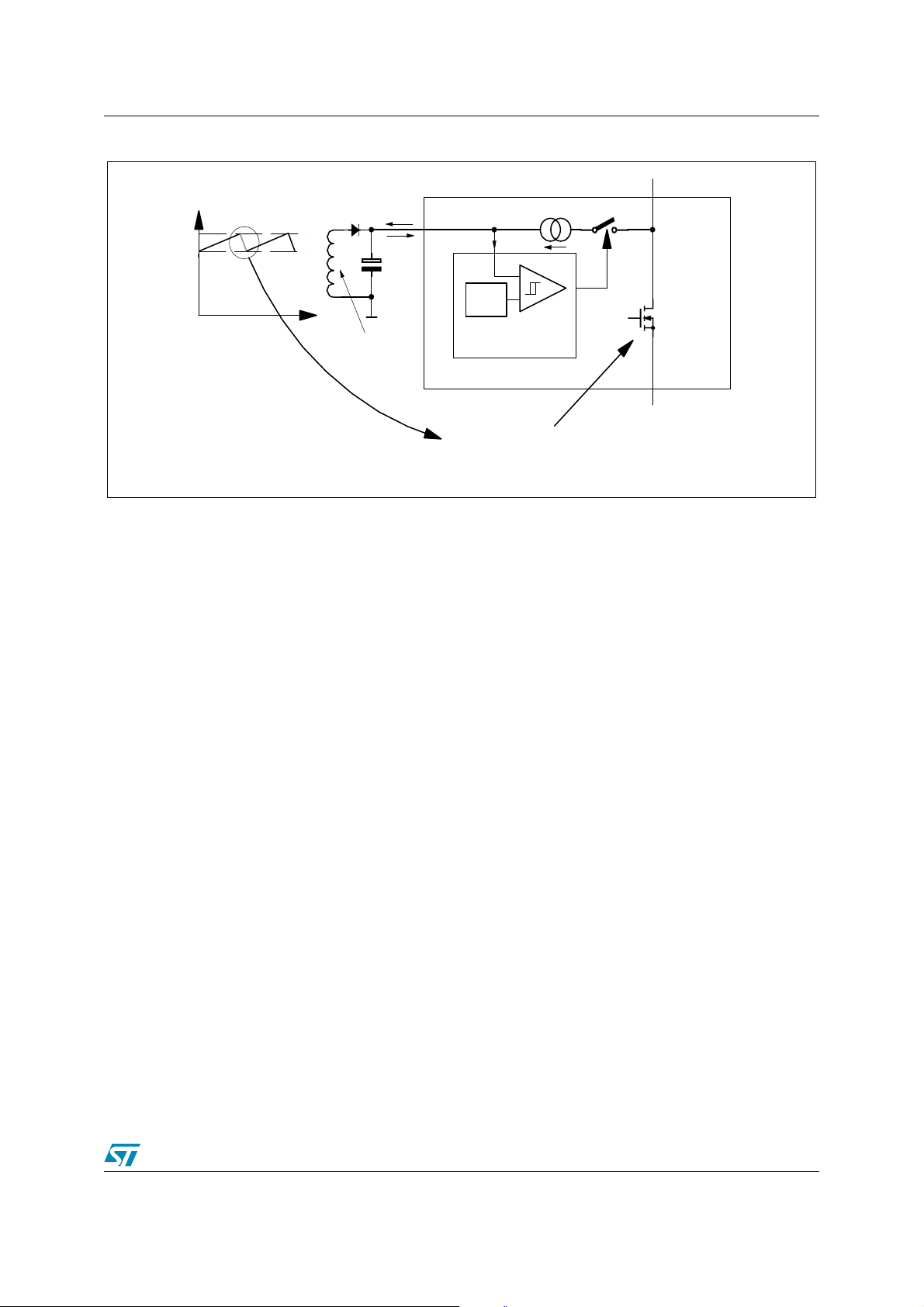
An integrated high voltage current source provides a bias current from the DRAIN pin during the start-up
phase. This current is partially absorbed by internal control circuits which are placed into a standby mode
with reduced consumption and also provided to the external capacitor connected to the V
as the voltage on this pin reaches the high voltage threshold V
of the UVLO logic, the device
DDon
becomes active mode and starts switching. The start-up current generator is switched off, and the
converter should normally provide the needed current on the V
pin through the auxiliary winding of the
DD
transformer, as shown on (see Figure 18).
In case there are abnormal conditions where the auxiliary winding is unable to provide the low voltage
supply current to the V
discharges to the low threshold voltage V
pin (i.e. short circuit on the output of the converter), the external capacitor
DD
of the UVLO logic, and the device goes back to the inactive
DDoff
state where the internal circuits are in standby mode a nd the start-up current source is activated. The
converter enters a endless start-up cycle, with a start-up duty cycle defined by the ratio of charging
current towards discharging when the V IPer100/100A tries to start. This ratio is fixed by design to 2A to
15A, which gives a 12% start-up duty cycle while the power dissipation at start-up is approximately 0.6W ,
for a 230Vrms input voltage.
This low value start-up duty cycle prevents the application of stress to the output rectifiers as well as the
transformer when a short circuit occurs.
pin. As soon
DD
The external capacitor C
to start up, when the device starts switching. This time t
on the VDD pin must be sized according to the time needed by the converter
VDD
depends on many param eters, among which
SS
transformer design, output capacitors, soft start feature, and compensation network implemented on the
COMP pin. The following formula can be used for defining the minimum capacitor needed:
where:
is the consumption current on the VDD pin when switching. Refer to specified I
I
DD
is the start up time of the converter when the device begins to switch. Worst case is gene rally at full
t
SS
C
and IDD2 values.
DD1
VDD
I
DDtSS
-------------------->
V
DDhyst
load.
V
is the voltage hysteresis of the UVLO logic (refer to the minimum specified value).
DDhyst
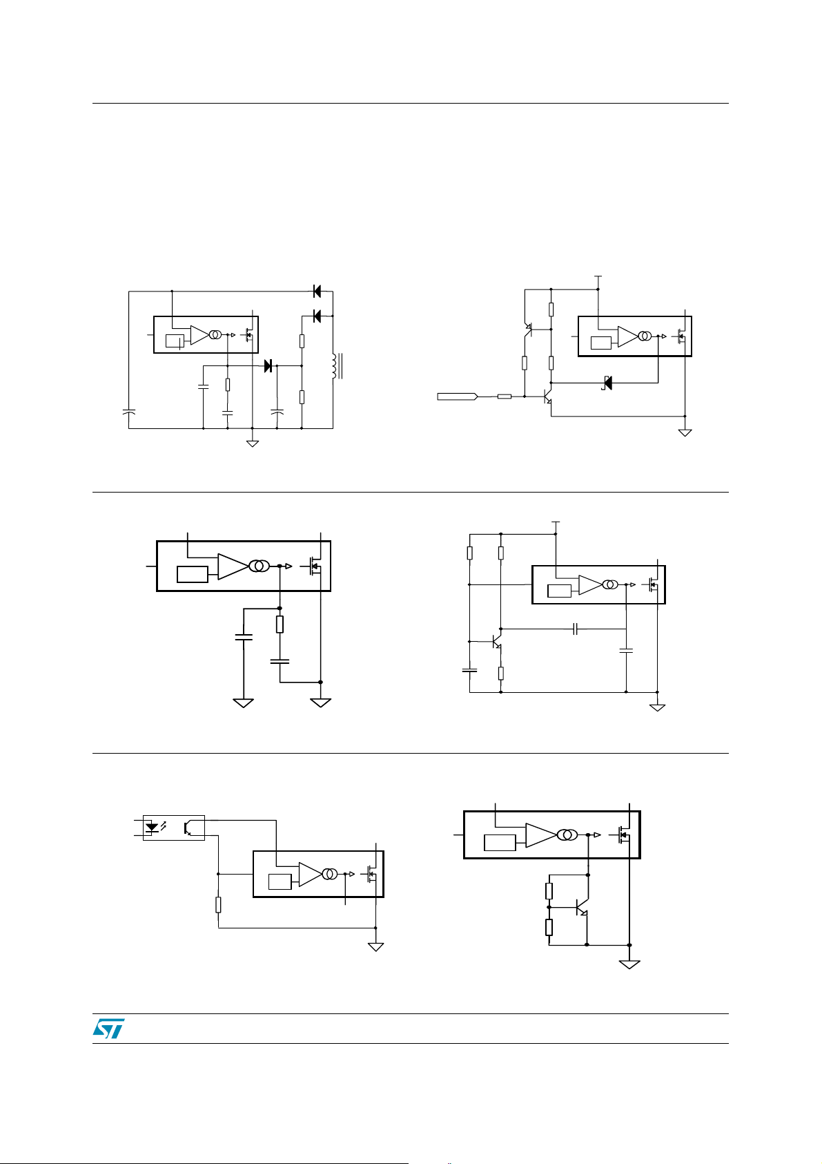
The soft start feature can be implemented on the COMP pin through a simple capacitor which will be also
used as the compensation network. In this case, the regulation loop bandwidth is rather low, because of
the large value of this capacitor. In case a large regulation loop bandwidth is mandatory, the schematics
of (see Figure 19) can be used. It mixes a high performance compensation network together with a
separate high value soft start capacitor. Both soft start time and regulation loop bandwidth can be
adjusted separately.
If the device is i ntentionally shut down by tying the COM P pin to ground, the device i s also performing
start-up cycle s, a nd the V
voltage is oscillating between V
DD
DDon
and V
DDoff
.
This voltage can be used for supplying external functions, provided that their consumption does not
exceed 0.5mA. (see Figure 20) page 17 shows a typical application of this function, with a latched
shutdown. Once the " Shutdown" sign al has bee n act ivated, the d evice remain s in th e Off state until the
input voltage is removed.
14/24
Page 15
VIPer100/SP - VIPer100A/ASP
E
V
Figure 18. Behaviour of the high voltage current source at start-up
VDDon
DDoff
VDD
t
Auxiliary prim a ry
winding
2 mA
15 mA
C
VDD
VDD
1 mA
Ref.
UNDERVOLTAGE
LOCK OUT LOGIC
3 mA
15 mA
VIPer100
Start up d u ty cycle ~ 12%
DRAIN
SOURC
FC00100
15/24
Page 16

VIPer 100/SP - VIPe r100A/A SP
G
I
P
----
Z
V
V
P
----
I
V
0.5–
----
V
R1R2+
--
Transconductance Error Amplifier
The VIPer100/100A includes a tran scond uc tance error amplifier. Transconductance Gm is the change in
output current (I
) versus change in input voltage (VDD). Thus:
COMP
∂
COM
=
------- --------- ----
m
V
∂
DD
The output impedance Z
This last equation shows that the open loop gain A
= Gm x Z
A
VOL
COMP
at the output of this amplifier (COMP pin) can be defined as:
COMP
∂
COMP
---------------- ------ ----
==
COMP
I
∂
CO MP
VOL
∂
1
m
-------- --------- -----
×
∂
COM
V
DD
--------G
can be rela ted to Gm and Z
COMP
:
where Gm value for VIPer100/100A is 1.5 mA/V typically.
is defined by specification, but Z
G
m
and therefore A
COMP
are subject to large tolerances. An
VOL
impedance Z can be connected between the COMP pin and ground in order to define the transfer
function F of the error amplifier more accurately, according to the following equation (very similar to the
one above):
F
= Gm x Z(S)
(S)
The error amplifier frequency response is reported in figure 10 page 8 for different values of a simple
resistance connected on the COMP pin. The unloaded transconductance error amplifier shows an
inter nal Z
of about 330KΩ. More complex impedance can be connected on the COMP pin to achieve
COMP
different compensation level. A capacitor will provide an integrator function, thus eliminating the DC static
error, and a resistance in series leads to a flat gain at higher frequency, insuring a correct phase margin.
This configuration is illustrated in (see Figure 21) page 17.
As shown in (see Figure 21) an additional noise filtering capacitor of 2.2nF is gene rally needed to avoid
any high frequency interference.
Is also possible to implement a slope compensation when working in continuous mode with duty cycle
higher than 50%. (see Figure 22) shows such a configuration. Note: R1 and C2 build the classical
compensation network, and Q1 is injecting the slope compen sation with the correct p olarity from the
oscillator sawtooth.
External Clock Synchronization:
The OSC pin provides a synchronisation ca pability when connected to an external frequency source.
(see Figure 23) page17 shows o ne possible schematic to be adapted, depending the s pecific needs. If
the proposed schematic is used, the pulse duration must be kept at a low value (500ns is sufficient) for
minimizing consumption. The optocoupl er must be able to provide 20mA through the optotrans istor.
Primary Peak Current Limita tion
The primary I
shown in (see Figure 24) page 18. The circuit based on Q1, R
pin in order to limit the primary peak current of the device to a value:
where:
=
COMP
The suggested value for R
16/24
current and, consequently, the output power can be limited us ing the simple circuit
DPEAK
0.6
×
-------- ---------R
2
is in the range of 220KΩ.
1+R2
and R2 clamps the voltage on the COMP
1
COMP
=
DPEAK
-------- --------- ------ --------H
ID
Page 17
VIPer100/SP - VIPer100A/ASP
Y
Over-Temperature Protection
Over-temperature protection is based on chip temperature sensing. The minimum junction temperature at
which over-temperature cut-out occurs is 140ºC, while the typical value is 170ºC. The device is
automatically restarted when the junction temperature decreases to the restart temperature threshold that
is typically 40ºC below the shutdown value (see Figure 11) page 8..
Figure 19. Mixe d Soft Start and Compensation Figure 20. Latched Shut Down
D2
U1
VIPER100
-
OSC
13V
+
C4
C3
+
DRAINVDD
COMP SOURCE
R1
C1
D1
D3
R3
AUXILIAR
WINDING
R2
C2
+
Shutdown
Q2
R4
R1
OSC
R2R3
Q1
U1
VIPER100
-
13V
+
D1
DRAINVDD
COMP SOURCE
FC00131
FC00110
Figure 21. Typical Compensation Network Figure 22. Slope Compensation
U1
VIPER100
OSC
13V
-
+
C2
DRAINVDD
COMP SOURCE
R1
C1
FC00121
C1 R3
R1R2
OSC
Q1
U1
VIPER100
-
13V
+
C2
DRAINVDD
COMP SOUR CE
C3
FC00141
Figure 23. External C l ock S in c hronisation F ig ure 24. Current Li m itation C i rcuit Example
U1
10 kΩ
OSC
13V
U1
VIPER100
-
+
DRAINVDD
COMP SOURCE
OSC
13V
VIPER100
-
+
R1
R2
DRAINVDD
COMP SOURCE
Q1
FC00220
FC00 240
17/24
Page 18
VIPer 100/SP - VIPe r100A/A SP
B
g
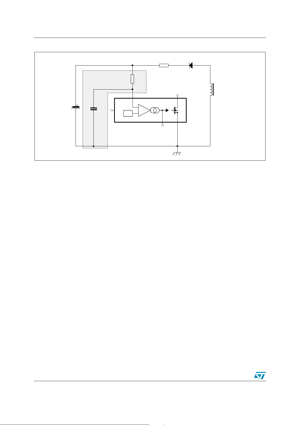
Figure 25. Input Voltage Surges Protection
R1
(Optional)
D1
R2
39R
Auxilliary windin
COMP
DRAIN
SOURCE
C1
ulk capaci to r
C2
22nF
OSC
VIPerXX0
13V
VDD
-
+
Electrical Over Stre ss Rugged n ess
The VIPer may be submitted to electrical over-stress, caused by violent input voltage surges or lightning.
Following the Layout Considerations is sufficient to prevent catastrophic damages most of the time.
However in some cases, the voltage surges coupled through the transformer auxiliary winding can
exceed the V
protection circuitry which cou ld be damage d by the stron g discharge current of t he V
The simple RC filter shown in (see Figure 25) page 17 can be implemented t o improve the application
immunity to such surges.
pin absolute maximum rating voltage value. Such events may trigger the VDD internal
DD
bulk capacitor.
DD
18/24
Page 19
VIPer100/SP - VIPer100A/ASP
d
d
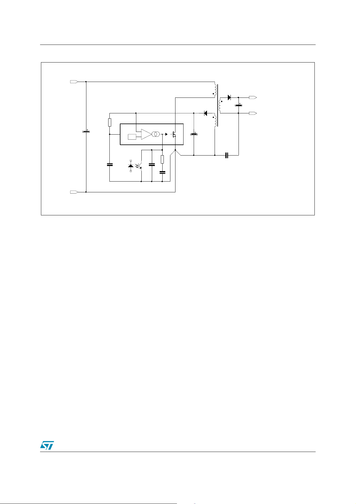
Figure 26. Recommended Layout
From input
iodes bridge
T1
D2
R1
C1
C2
OSC
U1
VIPerXX0
+
13V
C3
ISO1
DRAINVDD
C5
COMP SOURCE
R2
C4
D1
To secondary
C7
filtering a nd loa
C6
FC00500
Layout Considerations
Some simple rules insure a correct running of switching power supplies. They may be classified into two
categories:
- Minimizing power loops: The switched power current must be carefully analysed and the corresponding
paths must be as small an inner loop area as possible. This avoids radiated EMC noises, conducted EMC
noises by magnetic coupling, and provides a better efficiency by eliminating parasitic inductances,
especially on secondary side.
- Using different tracks for low level and power sig nals: Interference due to mixing of signal a nd power
may result in in stabilit ies and/ or anom alous behaviour of the device in case of violent power surge (Input
overvoltages, output short circuits...).
In case of VIPer , these rules apply as shown on (see Figure 26).
• Loops C1-T1-U1, C5-D2-T1, and C7-D1-T1 must be minimized.
• C6 must be as close as possible to T1.
• Signal components C2, ISO1, C3, and C4 are u sing a dedic ated track connected direct ly to the power
source of the device.
19/24
Page 20
VIPer 100/SP - VIPe r100A/A SP
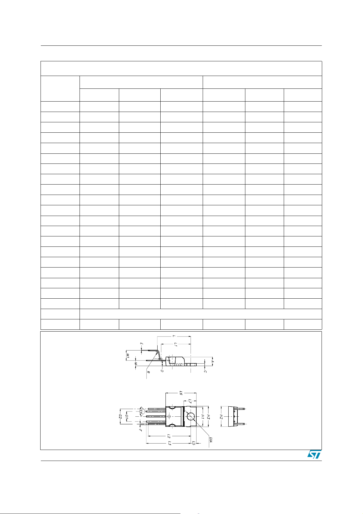
Pentawatt HV Mechanical Data
mm. inch
Dim
Min. Typ. Maw. Min. Typ. Max.
A 4.30 4.80 0.169 0.189
C 1.17 1.37 0.046 0.054
D 2.40 2.80 0.094 0.11
E 0.35 0.55 0.014 0.022
F 0.60 0.80 0.024 0.031
G1 4.91 5.21 0.193 0.205
G2 7.49 7.80 0.295 0.307
H1 9.30 9.70 0.366 0.382
H2 10.40 0.409
H3 10.05 10.40 0.396 0.409
L 15.60 17.30 6.14 0.681
L1 14.60 15.22 0.575 0.599
L2 21.20 21.85 0.835 0.860
L3 22.20 22.82 0.874 0.898
L5 2.60 3 0.102 0.118
L6 15.10 15.80 0.594 0.622
L7 6 6.60 0.236 0.260
M 2.50 3.10 0.098 0.122
M1 4.50 5.60 0.177 0.220
R0.50 0.02
V4 90
°
Diam 3.65 3.85 0.144 0.152
20/24
P023H3
Page 21
VIPer100/SP - VIPer100A/ASP
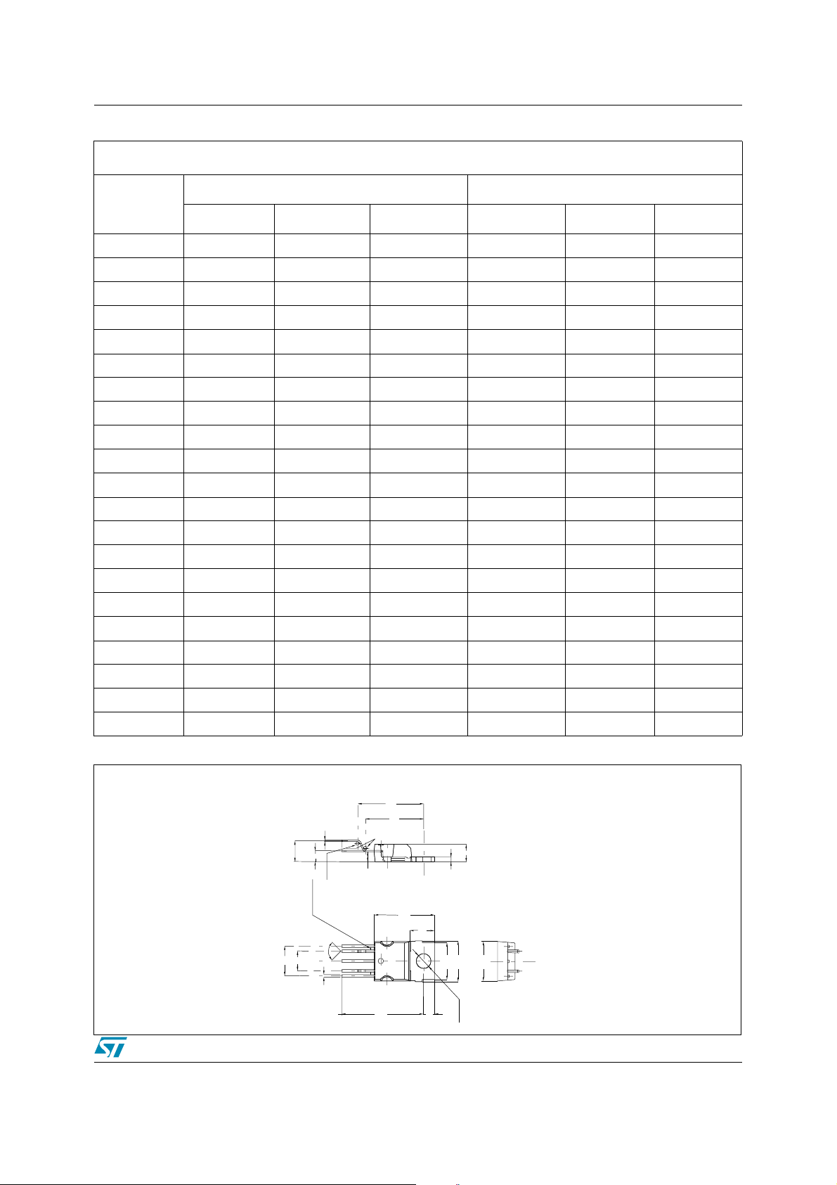
Pentawatt HV 022Y ( Vertical High Pitch ) Mechanical Data
mm. inch
Dim
Min. Typ. Maw. Min. Typ. Max.
A 4.30 4.80 0.169 0.189
C 1.17 1.37 0.046 0.054
D 2.40 2.80 0.094 0.110
E 0.35 0.55 0.014 0.022
F 0.60 0.80 0.024 0.031
G1 4.91 5.21 0.193 0.205
G2 7.49 7.80 0.295 0.307
H1 9.30 9.70 0.366 0.382
H2 10.40 0.409
H3 10.05 10.40 0.396 0.409
L 16.42 17.42 0.646 0.686
L1 14.60 15.22 0.575 0.599
L3 20.52 21.52 0.808 0.847
L5 2.60 3.00 0.102 0.118
L6 15.10 15.80 0.594 0.622
L7 6.00 6.60 0.236 0.260
M 2.50 3.10 0.098 0.122
M1 5.00 5.70 0.197 0.224
R 0.50 0.02 0.020
V4 90
° 90°
Diam 3.65 3.85 0.144 0.154
L
E
M1
M
R
Resin between
leads
G2
V4
G1
L1
A
D
L6
C
L7
H2
H3
H1
F
DIA
L3
L5
21/24
Page 22
VIPer 100/SP - VIPe r100A/A SP
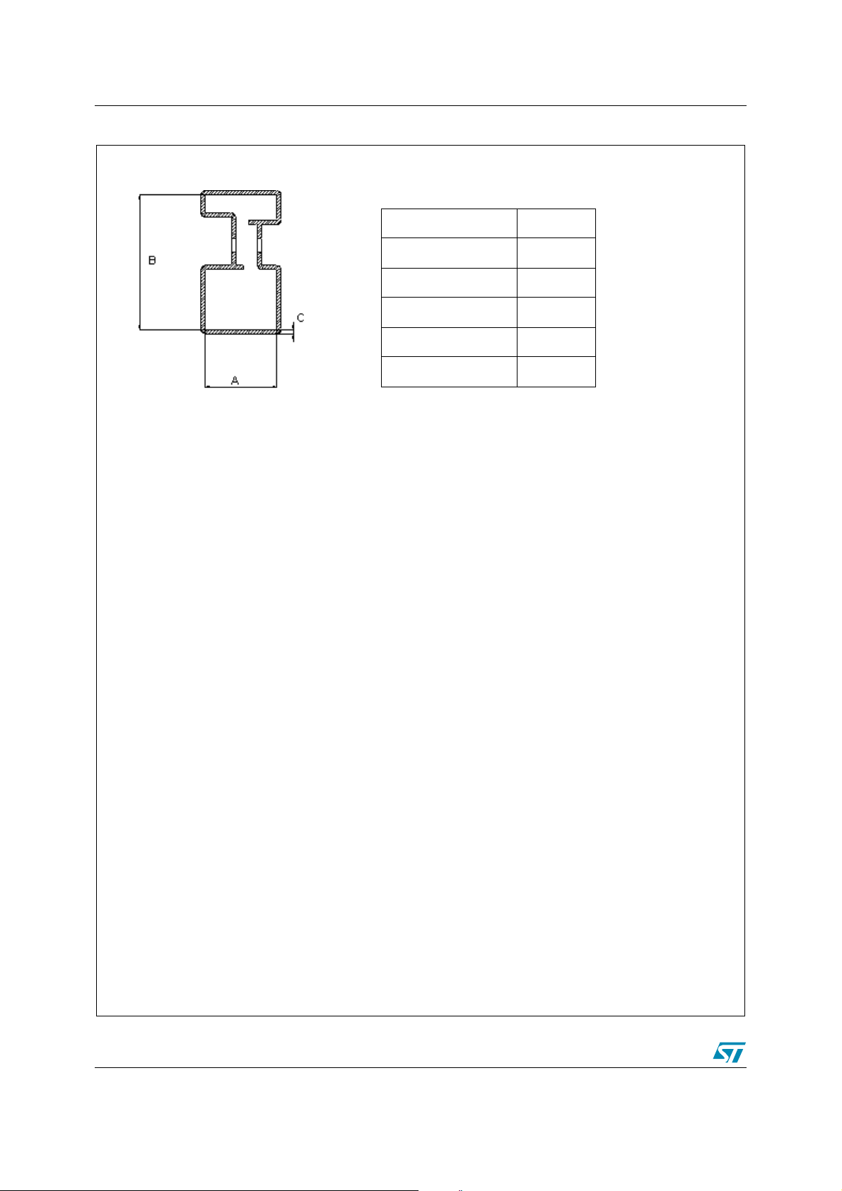
Figure 27. Pentawatt HV Tube Shipment ( no suffix )
Base Q.ty 50
Bulk Q.ty 1000
T ube length ( ± 0.5 ) 532
A 18
B 33.1
C ( ± 0. 1) 1
All dimensions ar e in mm.
22/24
Page 23

VIPer100/SP - VIPer100A/ASP
Table 13. Revision history
Date Revision Changes
02-May-2005 1 Initial release.
08-JUn-2005 2
Update without PowerSO-10
TM
23/24
Page 24

VIPer 100/SP - VIPe r100A/A SP
I
s
o
d
b
ct
t
ot
a
nformation furnished is believed to be accurate and reliable. However, STMicroelectronics assumes no responsibility for the consequence
f use of such information nor for any infringement of patents or other rights of third parties which may result from its use. No license is grante
y implic ation or oth erwise under any patent or patent rights of STMicroelectron i cs . Specificat i ons mentioned in thi s publication are sub je
o change without notice. This publication supersedes and replaces all information previously supplied. STMicroelectronics products are n
uthoriz ed for use as crit ical components in life support devices or s ystems without express written approval of STMicroelectron ics.
The ST logo is a registered trademark of ST M i croelectroni cs.
All other nam es are the prop erty of their respective owners
© 2005 STMi croelectro ni cs - All rights reserved
Austra l i a - Be l gi um - Brazil - C anada - China - Cze ch Republic - F i nl and - France - Germany - Hong K ong - India - Isr ael - Italy - Japan -
Malaysi a - M al ta - Morocco - Singapore - Sp ai n - Sweden - Swi tzerland - United Kingdom - United States of Ameri ca
STMicroelectronics group of com panies
www.st.com
24/24
 Loading...