

Page 1

INTEGRATED CIRCUITS
DATA SH EET
VES9600
Single Chip DVB-T Channel
Receiver
Product specification
File under Integrated Circuits, IC02
1999 Sep 01
Page 2

Philips Semiconductors Product specification
Single Chip DVB-T Channel Receiver VES9600
FEATURES
• 2K and 8K COFDM demodulator ( Fully
DVB-T compliant : ETS 300-744).
• All modes supported including
hierarchical modes.
• On chip 9-bit ADC.
• Digital down conversion.
• Fully automatic transmission parameters
detection.
• Crystal or VCXO clock generation.
• Frequency offset estimator to speed up
the scan.
• RF Tuner input power measurement
• On chip FEC decoder, full DVB-T
compliant.
• Parallel or serial transport stream
interface.
• DSP based synchronization.
• BER measurement
• SNR estimation
• Channel frequency response output.
• Channel impulse response output.
• Controllable dedicated I2C tuner bus.
• 2 low frequency spare DAC. (∆Σ)
• Spare I/O.
• I2C bus interface, for easy control.
• CMOS 0.35µm technology.
DESCRIPTION
The VES9600 is a single chip channel receiver for 2K and 8K
COFDM modulated signals based on the ETSI specification (ETSI
300 744). The device interfaces directly to an IF signal, which is
sampled by a 9-bit AD converter.
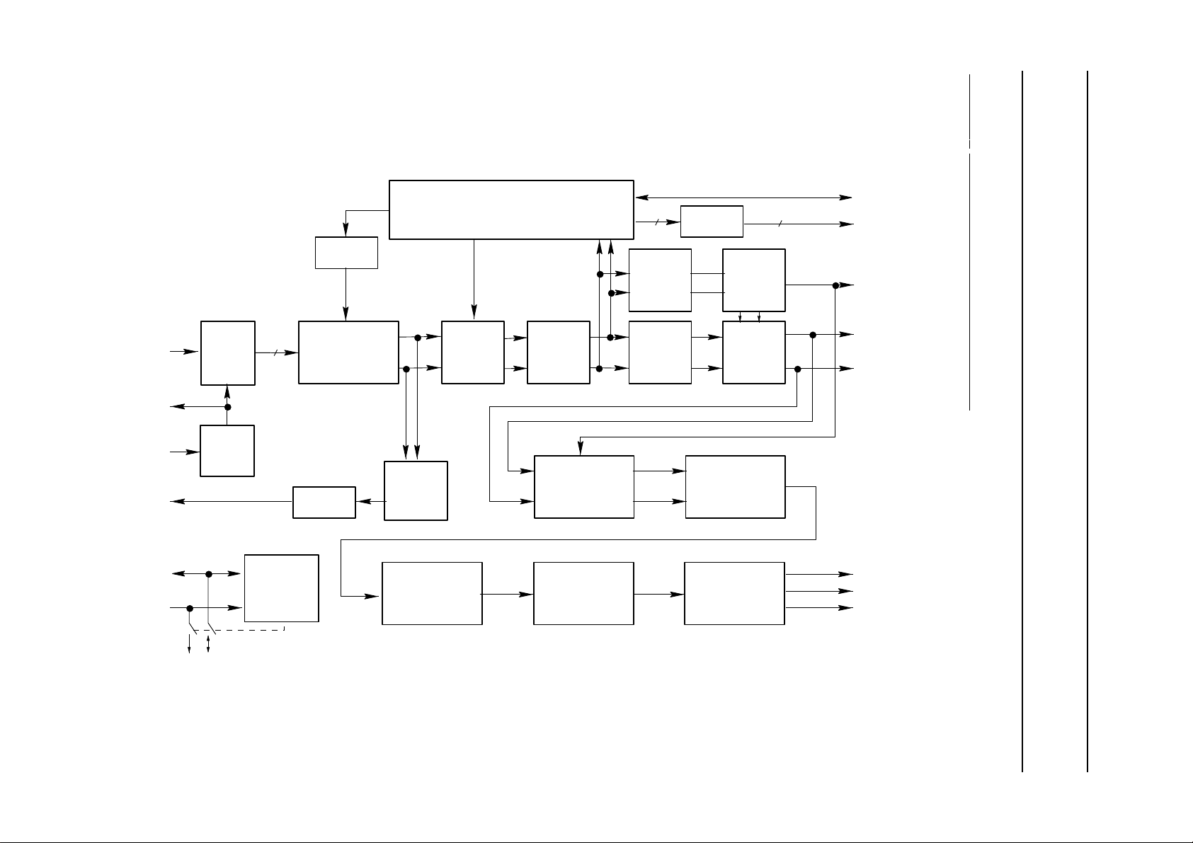
The VES9600 performs all the COFDM demodulation tasks from IF
signal to the MPEG2 transport stream. An internal DSP core
manages the synchronization and the control of the demodulation
process.
After base band conversion and FFT, the channel frequency
response is estimated based on the scattered pilots, and filtered in
both time and frequency domains. This estimation is used as a
correction on the signal, carrier by carrier. A common phase error
and estimator is used to deal with the tuner phase noise.
The FEC decoder is automatically synchronized thanks to the frame
synchronization algorithm that uses the TPS information included in
the modulation. Finally descrambling according to DVB-T standard,
is achieved at the Reed Solomon output.
This device is controlled via an I2C bus. The chip provides a
switchable tuner I2C bus to be disconnected from the I2C master
when not necessary. The DSP software code can be fed to the
chip via the master I2C bus or via a dedicated I2C bus (Eeprom).
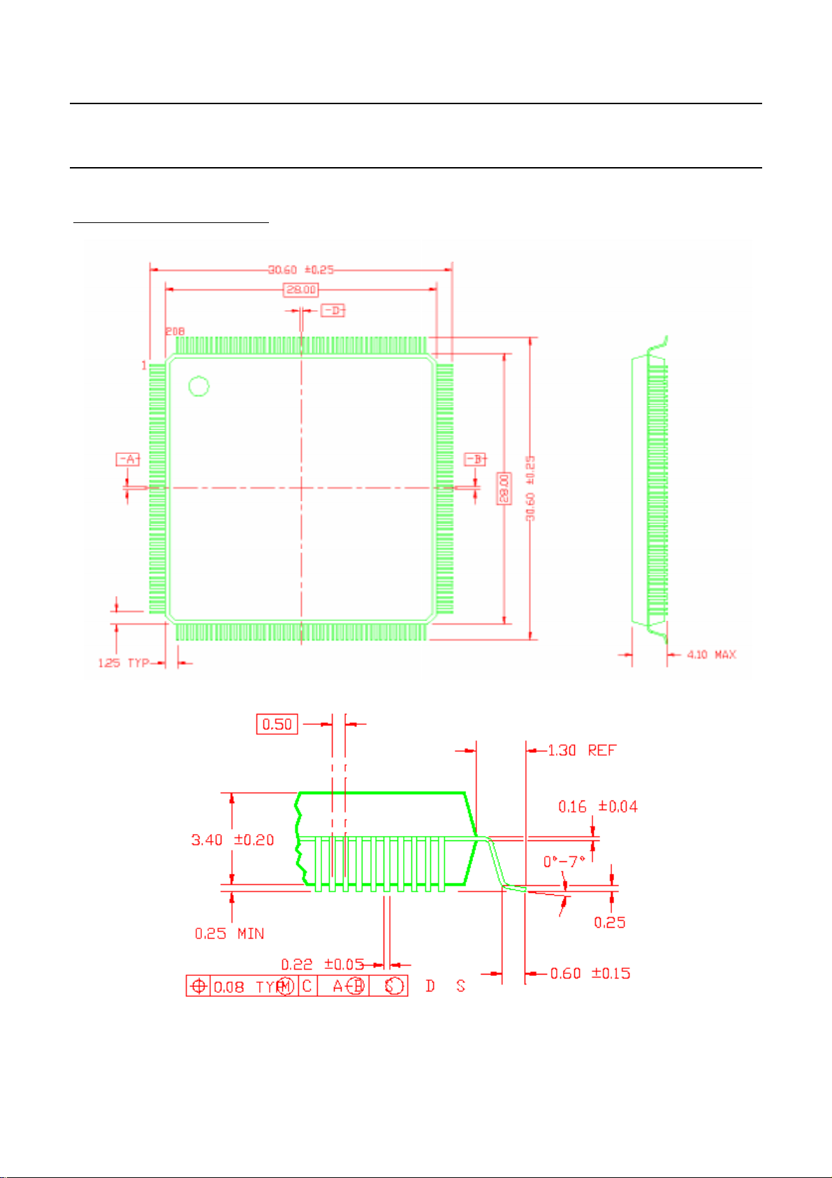
Designed in 0.35 µm CMOS technology and housed in a 208-pin
MQFP package, the VES9600 operates over the commercial
temperature range.
APPLICATIONS
• DVB-T fully compatible.
• Digital data transmission using
COFDM modulations.
1999 Sep 01 2
Page 3
1999 Sep 01 3
FIGURE 1 : FUNCTIONAL BLOCK DIAGRAM
Single Chip DVB-T Channel Receiver VES9600
Philips Semiconductors Product specification
IF
SACLK
XIN
O AGC
SDA
SCL
ADC
/2
9
2
IC
INTERFACE
NCO
BASE-BAND
CONVERSION
Σ/∆
OAK+ DSP CORE (XIN MIPS)
Frequency Timing framing recovery
CARRIER
RECOVERY
AGC
OUTER
DE-INTERLEAVER
FFT
INNER
DE-INTERLEAVER
R. S.
DECODER
10
CHANNEL
ESTIMATOR
CPE
3 Symbols
DELAY LINE
Σ/∆
TIMING
FREQUENCY
INTERPOLATOR
CORRECTION
VITERBI
DECODER
DE-SCRAMBLER
General purpose
digital inputs/outputs
3
analog outputs
CONFIDENCE
I
RECOV_DATA
Q
DO
OCLK
DEN
TO TUNER
Page 4

Philips Semiconductors Product specification
Single Chip DVB-T Channel Receiver VES9600
INPUT - OUTPUT SIGNAL DESCRIPTION
SYMBOL PIN NUMBER TYPE DESCRIPTION
CLOCK AND RESET SIGNALS
CLR# 32 I reset signal, active low
8
XIN
XOUT 9 O Crystal oscillator output pin.
SACLK
USE_NCO 33 I When low the chip is in VCXO mode else in NCO mode
CTRL_VCXO
CLK_X1
CLK_X2
25 O
26 O
181 O
180 O
I
(5V)
(5V)
(5V)
(5V)
Crystal oscillator input pin. When USE_NCO pin is high a third
overtone XTAL should be connected between the XIN and XOUT pins.
When USE_NCO pin is low a VCXO should be connected between
XIN and via a RC filter to the CTRL_VCXO output.
Sampling frequency output. This output clock can be fed to an
external (10-bit) ADC as sampling clock. SACLK= XIN/2
If not in NCO mode, control of an external sampling VCXO (after low-
pass filtering)
Internal SACLK equivalent monitoring output.
Internal SACLK* 2 equivalent monitoring output.
DEMODULATOR SIGNALS
FI[9:0] 12-13-14-15-16-
19-20-21-22-23
FFT_WIN_IN 81 I to be connected to FFT_WIN_OUT in default mode.
FFT_WIN_OUT 82 O
VAGC 27 O
RECOV_DATA
[7:0]
CFND[3 :0] 151-152-153-154 O
H2[3:0] 160-161-162-163 O
EN_CLK
D_START 145 O
D_VAL 144 O
FRAME 147 O
SUPER_FRAME 146 O
TPS_VAL 143 O
FEL
168-169-170171-172-173-
174-175
150 O
77 0
I Input data from an external ADC, FI must be tied to ground when not
used, positive notation (from 0 to 1023) or two’s complement notation
(from -512 to 511).
Output signal, indicating the start of the active data; equals 1 during
(3.3)
output value from the Delta-Sigma Modulator, used to control a log-
(5V)
O
Demodulator output signal (after channel correction), synchronous with
(3.3)
(3.3)
(3.3)
(3.3)
(3.3)
(3.3)
(3.3)
(3.3)
(3.3)
(5V)
the falling edge of CLK_X1, provided in a multiplexed way, I first.
Multiplexed output bearing the confidence factor during I and channel
response square amplitude during Q (4 MSB bits), respectively to
RECOV_DATA. (For the channel square amplitude see C2_H2)
4 LSB bits of the channel response square amplitude according to
enable clk18 to synchronize and phase the RECOV_DATA H2 et
CFND outputs. EN_CLK is set to 1 during I and 0 during Q.
Output signal, indicating the start of the active data out of the
equalizer; equals 1 during sample Kmin of the RECOV_DATA current
output block, for 2 18MHz clock cycles. CAUTION : sample Kmin does
not convey regular data, since it happens to be a continual carrier; it is
the first active (non zero) sample of the current OFDM block, but
active when RECOV_DATA corresponds to regular data .
Indicate the active data out of the first block in a frame at the
Same as FRAME in 8K; in 2K, active only on the first block of each
superframe. Indicates the beginning of a new SUPER-FRAME.
active when RECOV_DATA corresponds to TPS demodulated data .
front end lock. FEL is an output drain output and therefore requires an
complex sample 0 of the active FFT block
scaled amplifier (after analog filtering )
Normal order.
CFND.
D_VAL and TPS_VAL (see below) will be low.
demodulation part output. (RECOV_DATA)
external pull up resistor.
1999 Sep 01 4
Page 5

Philips Semiconductors Product specification
Single Chip DVB-T Channel Receiver VES9600
76
IT
DO[7:0] 118-119-120-
121-124-125-
126-127
OCLK 113 O
DEN 115 O
PSYNC 112 O
UNCOR 114 O
FSTART 109 O
108
DVIT
HVIT
107 O
(5V)
(3.3)
(3.3)
(3.3)
(3.3)
(3.3)
(3.3)
(3.3)
(3.3)
Interrupt line. This output interrupt line can be configured by the I2C
O
interface. See registers Itsel and Itstat. IT is an open drain output and
therefore requires an external pull up resistor.
FEC OUTPUTS
O
output data carrying the current sample of the current MPEG2 packet
(188 bytes), delivered on the rising edge of OCLK by default. When
the serial mode is selected, the output data is delivered by DO[0].
Output CLock. OCLK is the output clock for the parallel DO[7:0]
outputs. OCLK is internally generated depending on which interface is
selected.
output data validation signal active high during the valid and regular
data bytes (may be inverted, see serial bus description).
Pulse SYNChro. This output signal goes high on a rising edge of
OCLK when a synchro byte is provided, then goes low until the next
synchro byte (may be inverted).
RS error flag, active high on one RS packet if the RS decoder fails in
correcting the errors (may be inverted).
Frame start active high for one OCLK output clock cycle at the
beginning of a new superframe made of 272 OFDM symbols for the 2k
mode and made of 68 OFDM symbols for the 8k mode (may be
inverted as C3_psync).
viterbi output data stream, delivered on the rising hedge of HVIT. You
O
can also find the viterbi output on DO[0] after by-passing the RS and
the descrambling.
viterbi output data stream clock, according to DVIT.
ON-CHIP ADC SIGNALS
48
VIM
49
VIP
42
CMCAP
39
RBIAS
40
CMI
41
CMO
45
VREF
VREFP 44 O This is a positive voltage reference for the A/D converter. It is derived
I
I
I
I
O
O
O
Negative input to the A/D converter. This pin is DC biased to half
supply through an internal resistor divider (2x10K resistors). In order
to remain in the range of the ADC, the voltage difference between pins
VIP and VIM should be between -0.5 and 0.5 volts.
Positive input to the A/D converter. This pin is DC biased to half supply
through an internal resistor divider (2x10K resistors). In order to
remain in the range of the ADC, the voltage difference between pins
VIP and VIM should be between –0.5 and 0.5 volts.
This pin is connected to a tap point on an internal resistor divider used
to create CMO and CMI. An external capacitor of value 0.1µf should
be connected between this point and ground to provide good power
supply rejection from the positive supply at higher frequencies.
An external resistor of value 3.3k
pin and ground to provide good accurate bias currents for the analog
circuits on the ADC.
This pin provides the common-mode in voltage for the analog circuits
on the ADC. It is the buffered version of a voltage derived from an onchip resistor devider, and has a nominal value of 0.75 x VD3.
This pin provides the common-mode out voltage for the analog circuits
on the ADC. It is the buffered version of a voltage derived from an on-
chip resistor devider, and has a nominal value of 0.5 x VD3.
This is the output of an on-chip resistor divider. An exter nal capacitor
of value 0.1µf should be connected between this point and ground to
provide good power supply rejection from the positive supply at higher
frequencies. Reference voltages VREFP and VREFM are derived from
the voltage on VREF.
should be connected between this
1999 Sep 01 5
Page 6

Philips Semiconductors Product specification
Single Chip DVB-T Channel Receiver VES9600
from the voltage on pin VREF through an on-chip fully-differential
amplifier. The voltage on this pin is nominally equal to CMO + 0.25
volts.
43
VREFM
VD1 38 I Power supply input for the digital switching circuitry (3.3 typ).
VS1 37 I Ground return for the digital switching circuitry.
VD2 51 I Power supply input for the analog clock drivers (3.3V typ).
VS2 50 I Ground return for the analog clock drivers.
VD3 46 I Power supply input for the analog circuits (3.3V typ).
VS3 47 I Ground return for analog circuits.
VD4
VS4 36 I Ground return for the well guard ring that surrounds the ADC.
SCL 62 I I2C serial clock. Up to 700 kbit/s, in this functional mode, I2C slave
SDA 63 I/O I2C serial data inout, open drain I/O pad Up to 700 kbit/s, in this
SADDR[1:0]
SCL_TUN
SDA_TUN
SCL_EEP 66 O Extra I2C clock line to download DSP code from an external
SDA_EEP 67 I/O Extra I2C data bus to download DSP code from an external EEPROM.
52
206-207
64
65
O
I
I
O
I/O
This is the negative voltage reference for the A/D converter. It is
derived from the voltage on pin VREF through an on-chip fully-
differential amplifier. The voltage on this pin is nominally equal to
CMO- 0.25 volts.
Power supply input that connects to an n-well guard ring that
surrounds the ADC (3.3V typ).
I2C INTERFACES
device
functional mode, I2C slave device
SADDR[1:0] are the 2 LSBs of the I2C address of the VES9600. The
MSBs are internally set to 00010. Therefore the complete I2C address
of the VES9600 is (MSB to LSB): 0,0,0,1,0,SADDR[1], SADDR[0]
tuner I2C serial clock signal. Can be connected or not to the master
I2C bus. (open drain)
Tuner I2C data bus. Can be connected or not to the master I2C bus.
(open drain)
EEPROM. Optional mode. Can be connected to the master I2C Bus
, (open drain)
Optional mode. Can be connected to the master I2C Bus. (open drain)
204-205
EEPADDR[1:0]
EEPSP[1:0]
DOWNLOAD_M
ODE
DSP_BIST
SDI_TCK 194 I Oak+ DSP smart debug interface, SDI+ external JTAG clock
SDI_TDI 195 I Oak+ DSP smart debug interface, SDI+ JTAG serial output
SDI_TMS 196 I Oak+ DSP smart debug interface, SDI+ JTAG test mode select
SDI_TDO 197 O Oak+ DSP smart debug interface, SDI+ JTAG serial output
202-203
4 I processor control, Boot Mode
3
EEPRAD[1:0] are the 2 LSBs of the I2C address of the EEPROM in
mode boot alone. The MSBs are internally set to 00010. Therefore the
I
I
I
complete I2C address of the EEPROM is (MSB to LSB):
1,0,1,0,0,EEPADDR[1], EEPADDR[0]
I2C EEPROM bus speed (SCL_EEP) :
0 : 800Khz; 1 : 400Khz; 2 : 200Khz; 3 : 100Khz.
DSP SIGNALS
If 0 the DSP download its software from an external eeprom on the
dedicated I2C BUS SDA_EEP and SCL_EEP.
If 1 the software is downloaded via a host in the I2C register
CODE_IN. In this case no need of an external eeprom.
Boot on the bist mode to test the DSP RAM bank.
If good SP_OUT[0] = 1
In normal mode of operation, DSP_BIST must be grounded.
1999 Sep 01 6
Page 7
Philips Semiconductors Product specification
POWER SUPPLIES
VDD GND VCC VSi
4
VDi
4
Single Chip DVB-T Channel Receiver VES9600
(3.3)
SP_IN[3:0] 72-73-74-75 I Spare inputs
SP_OUT[7:0]
88-89-90-91-92-
93-94-95
CTRL[1:0] 84-85 O
DS_SPARE_1 28 O
DS_SPARE_2 29 O
TESTADC 55 I Must be set to “1”
TCK 187 I clock signal for boundary-scan. Wired to GND (if not used)
TDI 188 I Input port for boundary-scan. Wired to GND (if not used)
TMS 190 I Mode programming signal for boundary-scan. Wired to GND (if not
TRST 189 I Asynchronous reset signal for boundary-scan. Wired to GND (if not
TDO 191 O
O
(3.3)
(3.3)
(5V)
(5V)
(5V)
Spare outputs
control detection signal, flag monitoring outputs.
Spare delta-sigma output. Managed by the DSP to handle a low
frequency DAC. ( automatic first stage tuner AGC measurement for
example).
Spare delta-sigma output. Managed by the DSP or by an I2C register
to generate an analog level. (after a RC low-pass filter)
BOUNDARY SCAN
used)
used)
Output port for boundary-scan. NC (if not used)
GND 2-10-18-31-69-
GN
71-80-87-97117-123-134142-149-165-
177-183-193-201
VCC 1-30-68-79-192 VCC
5V
VDD 7-17-70-86-96-
116-122-133-
VDD
3.3V
141-148-164-
176-182-200
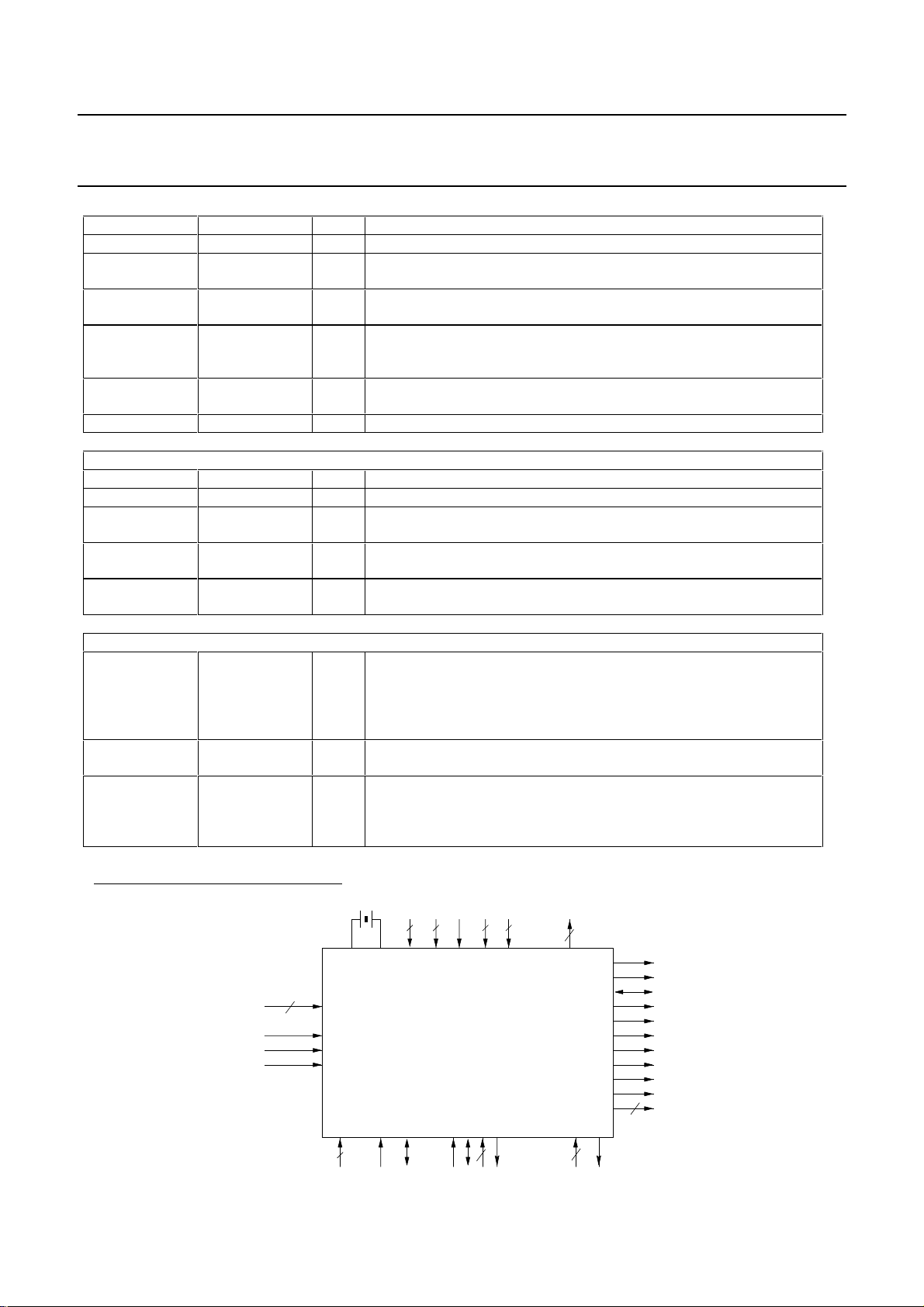
FIGURE 2 : BLOCK DIAGRAM
VIP
VIM
10
FI[9:0]
CLR#
XIN XOUT
INPUTS
INTERFACE
POWER SUPPLIES
Positive Power Supply 5 V typical
Positive Power Supply 3.3 V typical
VES9600
DSP_INTERFACE
Ground level 0 V
RECOV_DATA
24
MONITORING
OUTPUTS
8
JTAG
SACLK
VAGC
SDA_TUN
SCL_TUN
IT
FEL
PSYNC
UNCOR
DEN
OCLK
DO[7:0]
3
SADDR[1:0] SCL SDA
SDA_EEP
1999 Sep 01 7
3
SDI_TDO
4
TDO
Page 8

Philips Semiconductors Product specification
Single Chip DVB-T Channel Receiver VES9600
FIGURE 3 : PIN DIAGRAM
RECOV_DATA[7]
RECOV_DATA[6]
RECOV_DATA[3]
RECOV_DATA[2]
VDD
RECOV_DATA[0]
RECOV_DATA[1]
SP_OUT[5]
SP_OUT[6]
SP_OUT[7]
VSS
VDD
-
RECOV_DATA[4]
-
RECOV_DATA[5]
SP_OUT[3]
SP_OUT[0]
SP_OUT[2]
SP_OUT[1]
SP_OUT[4]
VSS
VDD
VDD
VSS--
H2[0]
H2[1]
-
H2[2]
H2[3]
-
-
-
157158159160161162163164165166167168169170171172173174175176177178179180181182183184185186187188189190191192193194195196197198199200201202203204205206207208
156
-
155
-
154
CFND[0]
153
CFND[1]
152
CFND[2]
CFND[3]
151
150
EN_CLK
149
VSS
148
VDD
147
FRAME
146
SUPER_FRAME
145
D_START
144
D_VAL
143
TPS_VAL
142
VSS
141
VDD
140
-
139
-
138
-
137
-
136
-
135
-
134
VSS
133
VDD
132
-
131
-
-
130
129
-
128
-
127
DO[0]
DO[1]
126
125
DO[2]
124
DO[3]
123
VSS
122
VDD
121
DO[4]
120
DO[5]
DO[6]
119
118
DO[7]
117
VSS
116
VDD
115
DEN
114
UNCOR
113
OCLK
112
PSYNC
111
-
110
-
109
FSTART
108
DVIT
107
HVIT
106
-
105
-
---
-
VCC
VSS
DSP_BIST
DOWNLOAD_MODE
VDD
XIN
XOUT
VSS
FI[9]
FI[8]
FI[7]
FI[6]
FI[5]
VDD
VSS
FI[4]
FI[3]
FI[2]
FI[1]
FI[0]
SACLK
CTRL_VCXO
VAGC
DS_SPARE_1
DS_SPARE_2
VCC
VSS
CLB#
USE_NCO
VS4
VS1
VD1
RBIAS
CMI
CMO
CMCAP
VREFM
VREFP
VREF
VD3
VS3
VIM
VIP
VS2
VD2
VD4
-
1
2
3
4
-
5
6
-
7
8
9
10
11
-
12
13
14
15
16
17
18
19
20
21
22
23
24
-
25
26
27
28
29
30
31
32
33
34
-
35
-
36
37
38
39
40
41
42
43
44
45
46
47
48
49
50
51
52
53 54 55 56 57 58 59 60 61 62 63 64 65 66 67 68 69 70 71 72 73 74 75 76 77 78 79 80 81 82 83 84 85 86 87 88 89 90 91 92 93 94 95 96 97 98 99 100101 102 103 104
EEPSPD[0]
EEPRAD[0]
EEPSPD[1]
EEPRAD[1]
SADDR[1]
SADDR[0]
TEST_ADC
SCL
-
SCL_TUN
SDA
SDI_TDO
SDI_TMS
SCL_EEP
SDA_TUN
SDI_TCK
SDA_EEP
VCC
SDI_TDI
-
VDD
VSS
TRST--
VSS
VCC
TDO
TMS
TDI
VES9600
SP_IN[2]
SP_IN[3]
VSS
VDD
VSS
TCK
IT
SP_IN[0]
SP_IN[1]
FEL
VSS
VDD
-
VSS
-
VCC
--CLK_X1
CLK_X2
CTRL[1]
-
FFT_WIN_OUT
FFT_WIN_IN
VSS
CTRL[0]
1999 Sep 01 8
Page 9

Philips Semiconductors Product specification
Single Chip DVB-T Channel Receiver VES9600
TABLE 1 : PIN DESCRIPTION
Pin Pin Name Direction
1VCC 2 VSS 3 DSP_BIST I
DWNLD_MODE
4
5- I
6- I
I
3
3
7VCC 8XIN I
9XOUT O
10 VSS 11 - I
3
12 FI[9] I
13 FI[8] I
14 FI[7] I
15 FI[6] I
16 FI[5] I
17 VCC 18 VSS 19 FI[4] I
20 FI[3] I
21 FI[2] I
22 FI[1] I
23 FI[0] I
24 - I
3
25 SACLK O
CTRL_VCXO
26
O
27 VAGC O
DS_SPARE_1
28
29
DS_SPARE_2
O
O
30 VCC 31 VSS 32 CLR# I
33 USE_NCO I
34 - I
35 - I
3
3
36 VS4 37 VS1 38 VD1 39 RBIAS I
40 CMI O
41 CMO O
42 CMCAP I
43 VREFM O
44 VREFP O
45 VREF O
46 VD3 47 VS3 48 VIM I
49 VIP I
50 VS2 51 VD2 52 VD4 53 - -
54 - 55 TEST_ADC I
56 - I
57 - O
58 - O
59 - O
60 - O
61 - O
62 SCL I
63 SDA I/O
64 SCL_TUN OD
65 SDA_TUN I/O
66 SCL_EEP OD
67 SDA_EEP I/O
68 VCC 69 VSS 70 VCC 71 VSS 72 SP_IN[3] I
73 SP_IN[2] I
74 SP_IN[1] I
75 SP_IN[0] I
76 IT OD
77 FEL OD
78 - I
79 VCC 80 VSS -
FFT_WIN_IN
81
FFT_WIN_OUT
82
83 - I
84 CTRL[1] O
85 CTRL[0] O
86 VDD 87 VSS 88 SP_OUT[7] O
89 SP_OUT[6] O
90 SP_OUT[5] O
91 SP_OUT[4] O
92 SP_OUT[3] O
93 SP_OUT[2] O
94 SP_OUT[1] O
95 SP_OUT[0] O
96 VDD 97 VSS 98 - I
99 - I
100 - I
101 - I
102 - I
103 - I
104 - I
105 - I
106 - I
107 HCORE O
108 DCORE O
3
3
3
3
3
3
3
1
I
O
3
3
3
3
3
3
3
3
3
3
109 FSTART O
110 - O
111 - I
112 PSYNC O
113 OCLK O
114 UNCOR O
115 DEN O
116 VDD 117 VSS 118 DO[7] O
119 DO[6] O
120 DO[7] O
121 DO[4] O
122 VDD 123 VSS 124 DO[3] O
125 DO[2] O
126 DO[1] O
127 DO[0] O
128 - I
129 - I
130 - I
131 - I
132 - O
133 VDD 134 VSS 135 - O
136 - O
137 - I
138 - I
139 - I
140 - I
141 VDD 142 VSS 143 TPS_VAL O
144 D_VAL O
145 D_START O
SUPER_FRAME
146
147 FRAME O
148 VDD 149 VSS 150 EN_CLK O
151 CFND[3] O
152 CFND[2] O
153 CFND[1] O
154 CFND[0] O
155 - I
156 - 157 - I
158 - I
159 - I
160 H2[3] O
161 H2[2] O
162 H2[1] O
163 H2[0] O
3
3
3
3
3
3
3
3
3
3
3
3
3
O
3
3
3
3
1999 Sep 01 9
Page 10

Philips Semiconductors Product specification
Single Chip DVB-T Channel Receiver VES9600
164 VDD 165 VSS 166 - O
167 - I
168
169
170
171
172
173
174
175
RECOV_DATA[7]
RECOV_DATA[6]
RECOV_DATA[5]
RECOV_DATA[4]
RECOV_DATA[3]
RECOV_DATA[2]
RECOV_DATA[1]
RECOV_DATA[0]
176 VDD 177 VSS 178 - O
179 - I
180 CLK_X2 O
3
3
O
O
O
O
O
O
O
O
3
3
181 CLK_X1 O
182 VDD 183 VSS 184 - 185 - O
186 - O
187 TCK I
188 TDI I
189 TRST I
190 TMS I
191 TDO OD
192 VCC 193 VSS 194 SDI_TCK I
95 SDI_TDI I
196 SDI_TMS I
197 SDI_TDO OD
198 - O
199 - O
200 VCC -
3
3
201 VSS 202 EEPSPD[1] I
203 EEPSPD[0] I
204 EEPRAD[1] I
205 EEPRAD[0] I
206 SADDR[1] I
207 SADDR[0] I
208 - I
Notes :
1.All inputs (I) are TTL, 5V tolerant inputs (excepted FFT_WIN_IN which is 3.3V only)
2.OD are Open Drain 5V outputs, so they must be connected to a pull-up resistor to either VDD or VCC
3. Test IO, inputs must be connected to GND.
3
3
3
1999 Sep 01 10
Page 11
Philips Semiconductors Product specification
Single Chip DVB-T Channel Receiver VES9600
PACKAGE INFORMATION
NOTE : Dimensions are in millimeters
1999 Sep 01 11
Page 12

Philips Semiconductors Product specification
Single Chip DVB-T Channel Receiver VES9600
DATA SHEET STATUS
DATA SHEET STATUS
PRODUCT
STATUS
DEFINITIONS
(1)
Objective specification Development This data sheet contains the design target or goal specifications for
product development. Specification may change in any manner without
notice.
Preliminary specification Qualification This data sheet contains preliminary data, and supplementary data will be
published at a later date. Philips Semiconductors reserves the right to
make changes at any time without notice in order to improve design and
supply the best possible product.
Product specification Production This data sheet contains final specifications. Philips Semiconductors
reserves the right to make changes at any time without notice in order to
improve design and supply the best possible product.
Note
1. Please consult the most recently issued data sheet before initiating or completing a design.
DEFINITIONS
Short-form specification The data in a short-form
specification is extracted from a full data sheet with the
same type number and title. For detailed information see
the relevant data sheet or data handbook.
Limiting values definition Limiting values given are in
accordance with the Absolute Maximum Rating System
(IEC 60134). Stress above one or more of the limiting
values may cause permanent damage to the device.
These are stress ratings only and operation of the device
attheseoratanyotherconditionsabovethosegiveninthe
Characteristics sections of the specification is not implied.
Exposure to limiting values for extended periods may
affect device reliability.
Application information Applications that are
described herein for any of these products are for
illustrative purposes only. Philips Semiconductors make
norepresentationorwarrantythatsuchapplicationswill be
suitable for the specified use without further testing or
modification.
DISCLAIMERS
Life support applications These products are not
designed for use in life support appliances, devices, or
systems where malfunction of these products can
reasonably be expected to result in personal injury. Philips
Semiconductorscustomersusingorsellingtheseproducts
for use in such applications do so at their own risk and
agree to fully indemnify Philips Semiconductors for any
damages resulting from such application.
Right to make changes Philips Semiconductors
reserves the right to make changes, without notice, in the
products, including circuits, standard cells, and/or
software, described or contained herein in order to
improve design and/or performance. Philips
Semiconductors assumes no responsibility or liability for
theuseofanyoftheseproducts,conveysnolicenceor title
under any patent, copyright, or mask work right to these
products,andmakesnorepresentationsorwarrantiesthat
these products are free from patent, copyright, or mask
work right infringement, unless otherwise specified.
2
PURCHASE OF PHILIPS I
C COMPONENTS
Purchase of Philips I
2
C components conveys a license under the Philips’ I2C patent to use the
components in the I2C system provided the system conforms to the I2C specification defined by
Philips. This specification can be ordered using the code 9398 393 40011.
1999 Sep 01 12
Page 13

Philips Semiconductors Product specification
Single Chip DVB-T Channel Receiver VES9600
NOTES
1999 Sep 01 13
Page 14

Philips Semiconductors Product specification
Single Chip DVB-T Channel Receiver VES9600
NOTES
1999 Sep 01 14
Page 15

Philips Semiconductors Product specification
Single Chip DVB-T Channel Receiver VES9600
NOTES
1999 Sep 01 15
Page 16

Philips Semiconductors – a w orldwide compan y
Argentina: see South America
Australia: 3 Figtree Drive, HOMEBUSH, NSW 2140,
Tel. +61 2 9704 8141, Fax. +61 2 9704 8139
Austria: Computerstr. 6, A-1101 WIEN, P.O. Box 213,
Tel. +43 1 60 101 1248, Fax. +43 1 60 101 1210
Belarus: Hotel Minsk Business Center, Bld. 3, r. 1211, Volodarski Str. 6,
220050 MINSK, Tel. +375 172 20 0733, Fax. +375 172 20 0773
Belgium: see The Netherlands
Brazil: seeSouth America
Bulgaria: Philips Bulgaria Ltd., Energoproject, 15thfloor,
51 James Bourchier Blvd., 1407 SOFIA,
Tel. +359 2 68 9211, Fax. +359 2 68 9102
Canada: PHILIPS SEMICONDUCTORS/COMPONENTS,
Tel. +1 800 234 7381, Fax. +1 800 943 0087
China/Hong Kong: 501 Hong Kong Industrial Technology Centre,
72 Tat Chee Avenue, Kowloon Tong, HONG KONG,
Tel. +852 2319 7888, Fax. +852 2319 7700
Colombia: see South America
Czech Republic: see Austria
Denmark: Sydhavnsgade 23, 1780 COPENHAGEN V,
Tel. +45 33 29 3333, Fax. +45 33 29 3905
Finland: Sinikalliontie 3, FIN-02630 ESPOO,
Tel. +358 9 615 800, Fax. +358 9 6158 0920
France: 51 Rue Carnot, BP317, 92156 SURESNES Cedex,
Tel. +33 1 4099 6161, Fax. +33 1 4099 6427
Germany: Hammerbrookstraße 69, D-20097 HAMBURG,
Tel. +49 40 2353 60, Fax. +49 40 2353 6300
Hungary: seeAustria
India: Philips INDIA Ltd, Band Box Building, 2nd floor,
254-D, Dr. Annie Besant Road, Worli, MUMBAI 400 025,
Tel. +91 22 493 8541, Fax. +91 22 493 0966
Indonesia: PTPhilips DevelopmentCorporation, Semiconductors Division,
Gedung Philips, Jl. Buncit Raya Kav.99-100, JAKARTA 12510,
Tel. +62 21 794 0040 ext. 2501, Fax. +62 21 794 0080
Ireland: Newstead, Clonskeagh, DUBLIN 14,
Tel. +353 1 7640 000, Fax. +353 1 7640 200
Israel: RAPAC Electronics, 7 Kehilat Saloniki St, PO Box 18053,
TEL AVIV 61180, Tel. +972 3 645 0444, Fax. +972 3 649 1007
Italy: PHILIPS SEMICONDUCTORS,ViaCasati, 23 - 20052 MONZA (MI),
Tel. +39 039 203 6838, Fax +39 039 203 6800
Japan: Philips Bldg 13-37, Kohnan 2-chome, Minato-ku,
TOKYO 108-8507, Tel. +81 3 3740 5130, Fax. +81 3 3740 5057
Korea: Philips House, 260-199 Itaewon-dong, Yongsan-ku, SEOUL,
Tel. +82 2 709 1412, Fax. +82 2 709 1415
Malaysia: No. 76 Jalan Universiti, 46200 PETALING JAYA, SELANGOR,
Tel. +60 3 750 5214, Fax. +60 3 757 4880
Mexico: 5900 Gateway East, Suite 200, EL PASO, TEXAS 79905,
Tel. +9-5 800 234 7381, Fax +9-5 800 943 0087
Middle East: see Italy
Netherlands: Postbus 90050, 5600 PB EINDHOVEN, Bldg. VB,
Tel. +31 40 27 82785, Fax. +31 40 27 88399
New Zealand: 2 Wagener Place, C.P.O. Box 1041, AUCKLAND,
Tel. +64 9 849 4160, Fax. +64 9 849 7811
Norway: Box 1, Manglerud 0612, OSLO,
Tel. +47 22 74 8000, Fax. +47 22 74 8341
Pakistan: see Singapore
Philippines: Philips Semiconductors Philippines Inc.,
106 Valero St. Salcedo Village, P.O. Box 2108 MCC, MAKATI,
Metro MANILA, Tel. +63 2 816 6380, Fax. +63 2 817 3474
Poland: Al.Jerozolimskie 195 B, 02-222 WARSAW,
Tel. +48 22 5710 000, Fax. +48 22 5710 001
Portugal: see Spain
Romania: see Italy
Russia: Philips Russia, Ul. Usatcheva 35A, 119048 MOSCOW,
Tel. +7 095 755 6918, Fax. +7 095 755 6919
Singapore: Lorong 1, Toa Payoh, SINGAPORE 319762,
Tel. +65 350 2538, Fax. +65 251 6500
Slovakia: see Austria
Slovenia: see Italy
South Africa: S.A. PHILIPS Pty Ltd., 195-215 Main Road Martindale,
2092 JOHANNESBURG, P.O. Box 58088 Newville 2114,
Tel. +27 11 471 5401, Fax. +27 11 471 5398
South America: Al. Vicente Pinzon, 173, 6th floor,
04547-130 SÃO PAULO, SP, Brazil,
Tel. +55 11 821 2333, Fax. +55 11 821 2382
Spain: Balmes 22, 08007 BARCELONA,
Tel. +34 93 301 6312, Fax. +34 93 301 4107
Sweden: Kottbygatan 7, Akalla, S-16485 STOCKHOLM,
Tel. +46 8 5985 2000, Fax. +46 8 5985 2745
Switzerland: Allmendstrasse 140, CH-8027 ZÜRICH,
Tel. +41 1 488 2741 Fax. +41 1 488 3263
Taiwan: Philips Semiconductors, 5F, No. 96, Chien Kuo N. Rd., Sec. 1,
TAIPEI, Taiwan Tel. +886 2 2134 2451, Fax. +886 2 2134 2874
Thailand: PHILIPS ELECTRONICS (THAILAND) Ltd.,
60/14 MOO 11, Bangna Trad Road KM. 3, Bagna, BANGKOK 10260,
Tel. +66 2 361 7910, Fax. +66 2 398 3447
Turkey: Yukari Dudullu, Org. San. Blg., 2.Cad. Nr. 28 81260 Umraniye,
ISTANBUL, Tel. +90 216 522 1500, Fax. +90 216 522 1813
Ukraine: PHILIPS UKRAINE, 4 Patrice Lumumba str., Building B, Floor 7,
252042 KIEV, Tel. +380 44 264 2776, Fax. +380 44 268 0461
United Kingdom: Philips Semiconductors Ltd., 276 Bath Road, Hayes,
MIDDLESEX UB3 5BX, Tel. +44 208 730 5000, Fax. +44 208 754 8421
United States: 811 East Arques Avenue, SUNNYVALE, CA 94088-3409,
Tel. +1 800 234 7381, Fax. +1 800 943 0087
Uruguay: see South America
Vietnam: see Singapore
Yugoslavia: PHILIPS, Trg N. Pasica 5/v, 11000 BEOGRAD,
Tel. +381 11 3341 299, Fax.+381 11 3342 553
For all other countries apply to: Philips Semiconductors,
Marketing Communications, Building BE-p, P.O. Box 218, 5600 MD EINDHOVEN,
The Netherlands, Fax. +31 40 27 24825
© Philips Electronics N.V. SCA
All rights are reserved. Reproduction in whole or in part is prohibited without the prior written consent of the copyright owner.
The information presented in this document does not form part of any quotation or contract, is believed to be accurate and reliable and may be changed
without notice. No liability will be accepted by the publisher for any consequence of its use. Publication thereof does not convey nor imply any license
under patent- or other industrial or intellectual property rights.
2000
Internet: http://www.semiconductors.philips.com
70
Printed in The Netherlands 753504/02/pp16 Date of release: 1999 Sep 01 Document order number: 9397 750 07147
 Loading...