

Page 1

comatlas S.A., 30 rue du Chêne Germain, BP 814, 35518 CESSON SEVIGNE Cedex, France
Phone : + 33 2 99 27 55 55 – Fax : +33 2 99 27 55 27, Internet : www.comatlas.fr / VES 1848 rev 1.2 / July 99
VES 1848
SINGLE CHIP
DAVIC / DVB-RC
CABLE MODEM
FEATURES
•
Fully compliant ETS300800 and DA VIC 1.2
•
Out-Off Band demodulation scheme :
-
On chip 7-bit ADC.
-
DQPSK demodulator.
-
Roll-off factor = 0.3 .
-
Direct IF sampling.
-
Variable bit rate from 1 to 12 Mbit/s (SAW
@ 8MHz BW).
-
Automatic Gain Control PWM output.
-
Descrambler.
-
Frame synchronization.
-
Deinterleaver.
-
RS decoder (55,53) .
•
In Band scheme :
-
Parallel or serial MPEG2 Transport Stream
inputs.
-
MAC PID filtering.
-
DAVIC ATM cells transmission supported.
•
Up-Stream synchronizati on.
•
Up-Stream modulation scheme :
-
Burst QPSK/16QAM modulator.
-
Roll-off factor = 0.25/0.3 .
-
Programmable preamb le valu e.
- Programmable burst length.
- Direct IF synthesys from 5 to 46 MHz.
- I and Q base band outputs provided.
- Variable bit rate from 256kbit/s to 16Mbit/s.
- Programmable RS encoder.
- Scrambler.
- On chip 10 bit DACs.
• External MAC functionality.
• Package 208 MQFP.
• CMOS technology (0.35µm, 3.3V).
APPLICATIONS
•
Cable modem.
•
DVB interactive set-top box.
•
DAVIC ATM cable physical layer.
DESCRIPTION
Based on the DVB-RC cable and DAVIC
specifications, the VES 1848 allows interactive
communication through HFC network between settop boxes and headends.
For Down Stream (DS) channel the circuit
implements a differe ntial QPSK dem odulator (Out Of
Band application) and accepts MPEG2 Transport
Stream inputs from a DS QAM demodul ator (In Band
application). This channel allows to synchronize the
Up Stream (US) cha nnel and to provide data to the
MAC layer which remains external.
The US channel is highly programmable and built
around a digital burst QPSK or 16QAM modulator
with direct IF synthesys or I and Q base band
outputs. The modulator is fully DVB and MCNS
compliant thanks to its burst profile programmation
(burst length, preamble, RS encoder, scrambler, bit
rate …).
The VES 1848 is packaged in a 208 MQFP, and
operates over the commercial temperature 0-70°C.
Page 2

comatlas reserves the right to make any change at any time without notice. VES 1848 rev 1.2 / July 99 / p 2
SUMMARY
CAUTION
This document is preliminary and is subject to change. Contact a
comatlas representative to determine if this is the current information
on this device.
The information containe d in this docu ment has bee n carefully ch ecked and is believed to be reliable. How ever,
comatlas makes no guarantee or warranty concerning the accuracy of said information and shall not be
responsible for any loss or damage of whate ver nature resulting fr om the use of, or reli ance upon, it. comatlas
does not guarantee that the use of an y informat ion contained herein wil l not infringe upon the p atent, tradem ark,
copyright, mask work right or other rights of third parties, and no patent or other license is implied hereby.
This document does not in any way extend comatlas warranty on any product beyond that set forth in its
standard terms and conditions of sale. comatlas reserves the right to make changes in the products or
specifications, or both, presented in this publication at any time and without notice.
LIFE SUPPORT APPLICATIONS : comatlas products are not intended for use as critical components in life
support applian ces, devic es, or sy stems i n which t he failur e of a comatlas product to perform could be expe cted
to result in personal injury.
Page 3
comatlas reserves the right to make any change at any time without notice. VES 1848 rev 1.2 / July 99 / p 3
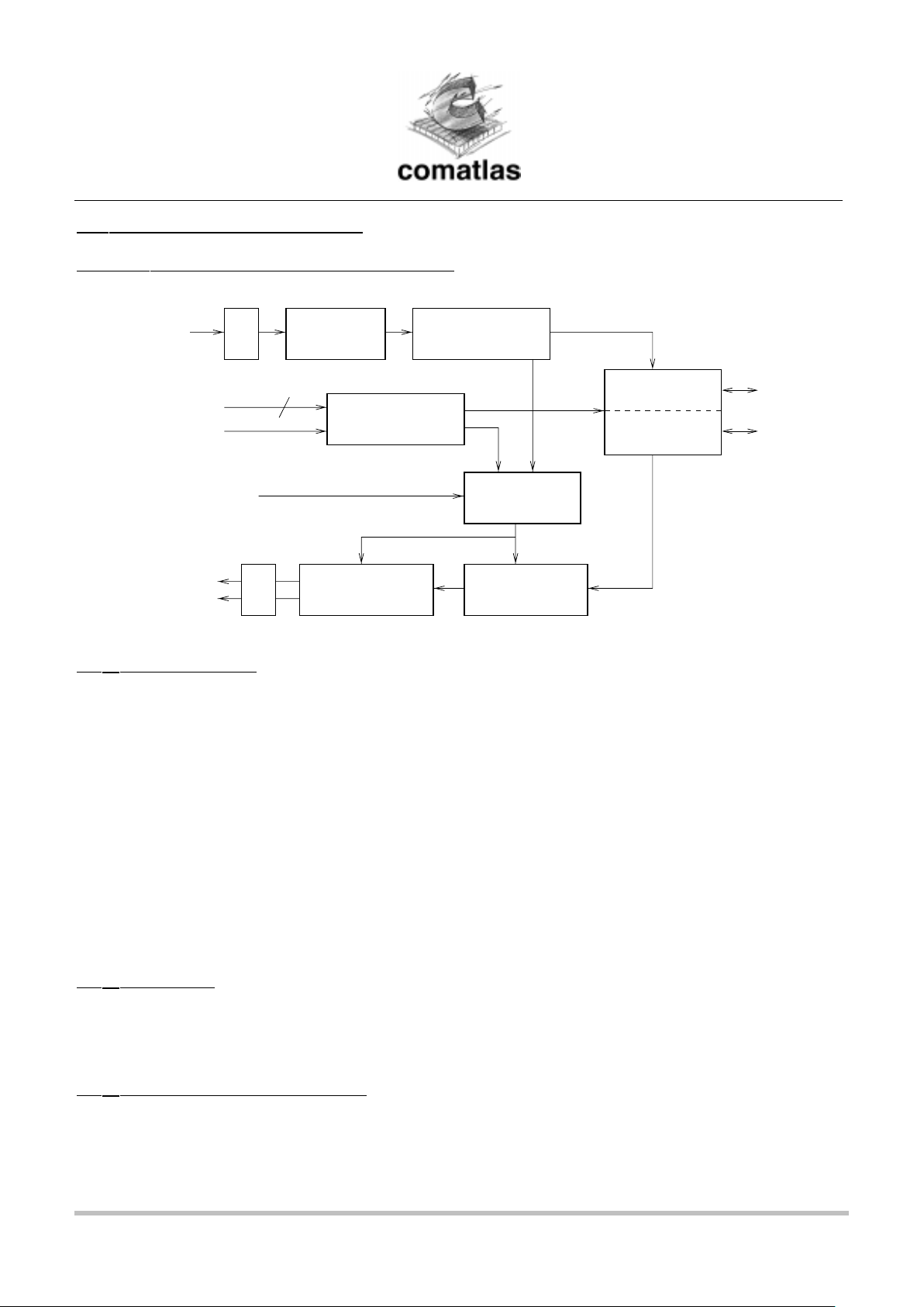
1 GENERAL DESCRIPTION
FIGURE 1 : FUNCTIONAL BLOCK DIAGRAM
interface
application layers
interface
MAC
Up Stream
synchronisation
external
synchro
channel processing
Out Of BandDQPSK
demodulator
ADC
IF
fixed
QPSK / 16QAM
burst modulator
DAC
Q
Up Stream
channel encoding
programmable
In Band
channel processing
symbol clock
MPEG2-TS
IF or I
1.1 ABREVIATIONS
AGC Automatic Gain Control
BW Bandwidth
CRC Cyclic Redundancy Checking (type of error correction code)
DS Down Stream (from the Headend to the set-top box)
HE Headend
HEC Header Error Control (CRC of the ATM cell header)
IB In Band
IF Intermediate Frequency
NIU Network Interface Unit (physical and MAC layers of the STB)
OOB Out Of Band
PWM Pulse Wave Modulation
SL-ESF Signalling Link Extended SuperFrame (name of the OOB frame)
STB Set-Top Box
US Up Stream (from the set-top box to the headend)
UW Unique Word (=preamble)
1.2 NOTATION
References to programmation registers are done this way :
AD.7 = bit 7 (in decimal) of the register located at the address AD (in hexa).
AD.[7-5] = bits 7 down to 5 of the register located at the address AD.
1.3 FUNCTIONAL DESCRIPTION
½ ADC
The VES 1848 implements a 7-bit analo g to digital converter. It directly sample s the OOB IF signal. The IF value
can be chosen by the system designer .
Page 4

comatlas reserves the right to make any change at any time without notice. VES 1848 rev 1.2 / July 99 / p 4
½ DQPSK DEMODULATOR
Fully digital variable bitrate demodulator used for the OOB channel. It implements a digital down conversion to
base band, filtering and decimat ion, frequency and clock recoveries as well as equalization. It also provides an
AGC command to the OOB tuner.
½ OOB CHANNEL PROCESSING
After descrambling, de framing and dein terleaving, ATM ce lls are fed into the RS decoder and correc ted. A filt ering
on ATM headers and MAC headers is the n d one on valid cells to keep onl y t hose addressed to the STB . M AC c e ll s
and application layers cell s are stored in 2 differ ent FIFOs. Up to 4 different VP I-VCI can b e filtered for applicatio n
layers data.
Mbits and Rxbits
(1)
are also output after integrity checking.
For US synchronization, 3ms mar k ers ar e gener at ed.
½ IB CHANNEL PROCESSING
This block is fed with the outputs of a cable FEC d ec oder. It i mp lem ent s t he f iltering of the MAC data addr e s sed to
the STB as well as valid time references and valid Rxbits filtering.
Mbits, Rxbits (after integrity checking) and MAC data are stored in a FIFO.
For US synchronization, 3ms mar k ers ar e gener at ed.
No PID filtering is done for application layers data.
This block implements the filtering of ATM cells transported in MPEG2-TS packet as defined by DAVIC. These data
are stored in the application layers FIFO and up to 4 different VPI-VCI can be filtered.
½ INTERFACES
MAC messages and application layers data are stored in different FIFO s. They can then be read/write with the
same or 2 different micro processor interfaces.
The VES 1848 registers are programmed with the MAC interface.
½ US SYNCHRONIZATION
This block decides when to send an US burst.
When the VES 1848 is used in a DVB/DAVIC device , th is bl oc k also doe s the propagation de la y com pen sa tion and
the US slot numberin g. It uses information fr om the DS channel (Mb its, 3ms markers) an d some provided by the
MAC layer (time compensation, slot number where to send a burst).
When the US path is u sed in a MCNS device, the burst start information is prov ided by the toggle of the external
synchro pin.
½ US CHANNEL ENCODING
It is DVB/DAVIC and MCNS compliant than ks to its burst profile programmatio n (6 different profiles can be stored
in the VES 1848).
Data read in FIFOs are RS e ncoded, rand omized and diff erential e ncoded before the addit ion of a p rogrammable
preamble.
½ BURST MODULATOR
Data can be output either in base band after predistorsion and nyquist filtering or directly on a programmable IF. In
that case a programmable sinewav e can al so be gen er ate d if requir ed .
½ DAC
Two 10-bit Digital to Analog Converters are built in the VES 1848. The modulated data are provided on both analog
and digital outputs.
(1)
refer to the DVB or DAVIC specification for the definition of Mbits and Rxbits.
Page 5
comatlas reserves the right to make any change at any time without notice. VES 1848 rev 1.2 / July 99 / p 5
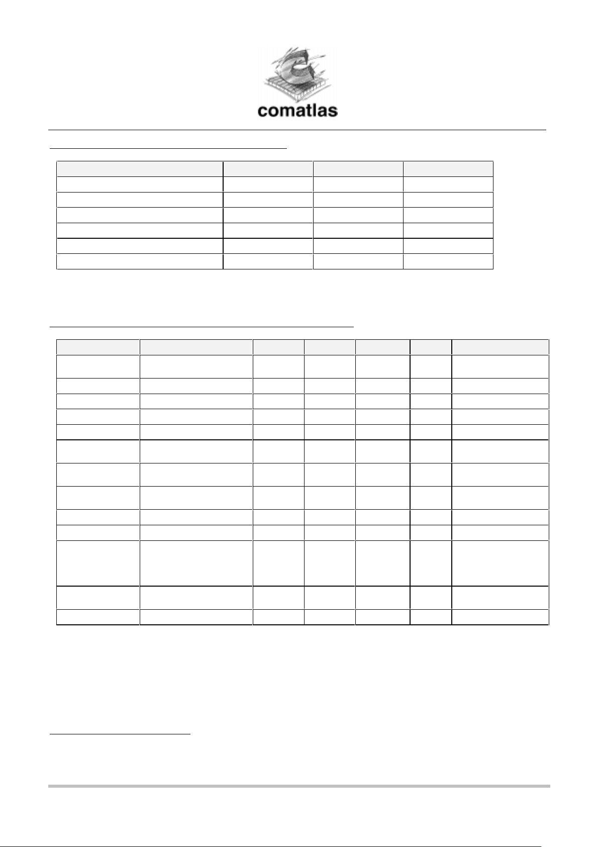
TABLE 1: ABSOLUTE MAXIMUM RATINGS
Parameter Min Max Unit
Ambient operating temperature : Ta 0 70 °C
DC supply voltage (VDD) - 0.5 + 4.1 V
DC Input voltage - 0.5 VDD + 0.5 V
DC Input Current ± 20 mA
Lead Temperature +300 °C
Junction Temperature +150 °C
Stresses above the abso lute max im um ratin gs ma y caus e perm ane nt dam age to the de vi ce. E xpo sur e to
absolute maximum ratings conditions for extended periods may affect device reliability.
TABLE 2 : RECOMMENDED OPERATING CONDITIONS
Symbol Parameter Min Typ Max Unit Notes
VDD
VD1, VD1IQ
Digital supply voltage 3.14 3.3 3.46 V 3.3V ±5%
VCC 5V supply 4.75 5 5.25 V
5V ± 5%
Ta Operating temperature 0 70 °C Ambient temperature
VIH
(1)
High-level input voltage 2 VCC + 0.3 V TTL input
VIL Low-level input voltage -0.5 0.8 V TTL input
VOH
(2)
High-level output voltage VDD -0.1
2.4
V @ IOH = -0.8 mA
@ IOH = + 2mA
VOL Low-level output voltage 0.1
0.4
V @ IOL = 0.8 mA
@ IOL = + 2mA
IDD + ICC Supply current 300 mA @US_clk = 116MHz
(3)
CIN Input capacitance 15 pF
COUT Output capacit an ce 15 pF
VD2
VD3, VD4
AVDDI, AVDDQ
VD0I, VD0Q
Analog supply voltage 3.14 3.3 3.46 V 3.3V ± 5%
I
FS
DAC full scale output
current range
25 mA
R
L
DAC termination resistor 75 ohms
(1)
All inputs are 5V tolerant.
(2)
IOH, IOL = ± 4mA only for pins DATAA, DATAM, INTA, INTM, VAGC, PWM2, FCONTI, SDAOUT, SDAIN,
SCLOUT, WRNA, RDN_ENAA, CSA, US_SACLK.
(3)
with the US modulator working in continuous mode and wit h direct IF sy nth es ys.
Page 6
comatlas reserves the right to make any change at any time without notice. VES 1848 rev 1.2 / July 99 / p 6
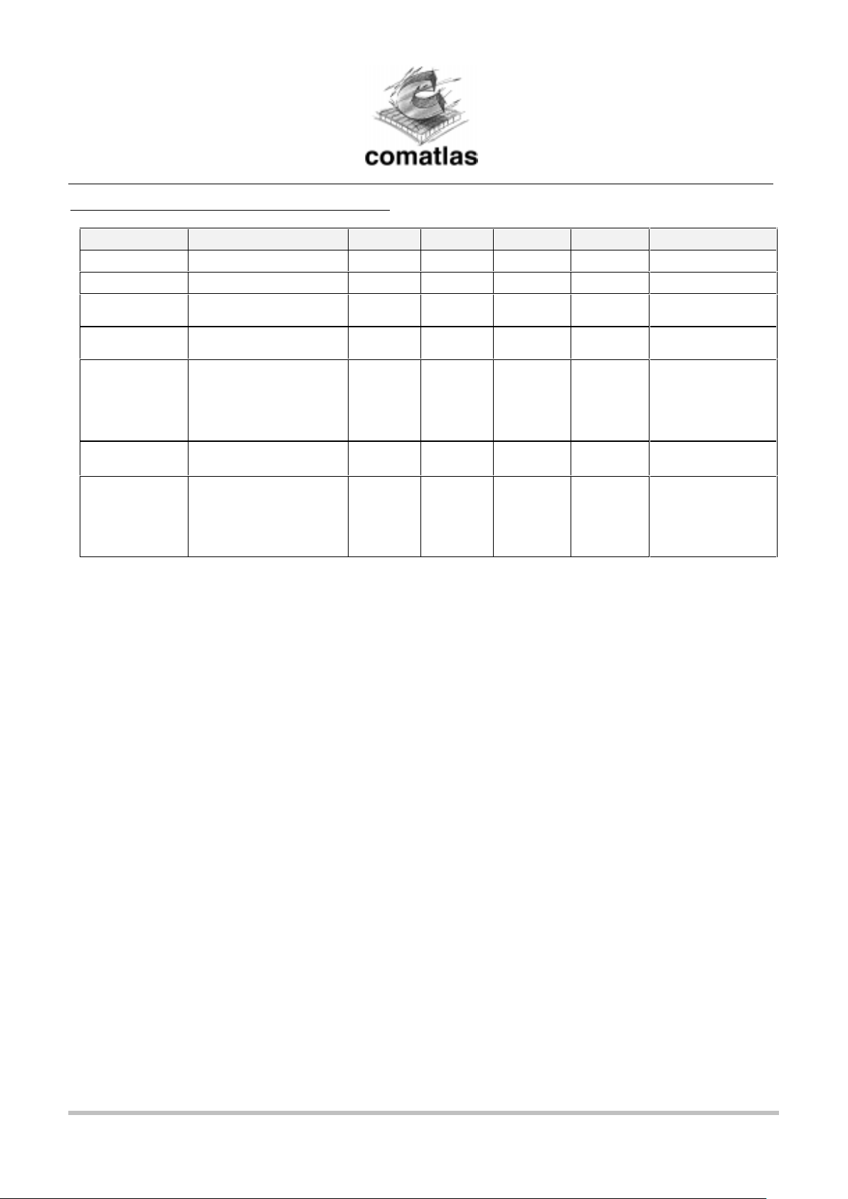
TABLE 3 : ANALOG CHARACTERISTICS
Symbol Parameter Min Typ Max Unit Notes
VIP-VIM ADC input signal range -0.5 0.5 V
ADC Rin ADC input Resistance 3 kohms
ADC Cin ADC capacitance
(VIP or VIM)
510pf
ADC BW OOB ADC input full
power bandwidth
40 50 MHZ 0.1dB bandwith
I
FS147
DAC full scale output
current
(on Iana and Qana)
17 18 19 mA VrefIQ=1.235V
IrefI and irefQ
connected to a
147Ω resistor,
US_clk = 60MHz
Voc DAC output voltage
compliance
0 1.0 1.05 V
Vout ≤ 1.0V
R
L
≤ 75 ohms
SFRD DAC spurious Free
Dynamic Range
-50 DBc RL = 37.5 ohms
US_clk = 58 MHz
Input data
frequency
= 0.3 US_clk
Page 7

comatlas reserves the right to make any change at any time without notice. VES 1848 rev 1.2 / July 99 / p 7
FIGURE 2 : INPUT-OUTPUT BLOCK DIAGRAM
VIM
VIP
OOB_dig
7
scan_en IDDQ test SCLin SDAin
SDAoutSCLoutTmode
switchtest
OOB analog
OOB_clk_in
OOB_clk_out
US_clk_in
US_clk_out
Doob
clk_OOB
OOB_saclk
vagc
PWM2
IBsymbclk
IBclk
IB
Psync
8
power supplies
VDD VSS VCC
1510
Iana
3
3
EXT_SYNC
Fconti
Iconti
Qconti
on_off
PctrPWM
10
10
Qana
Q
US_saclk
I_IF
OOB
IB
US
VES1848
dataM
8
intM
hmuxmodeM
hstbmodeM
csM
rdn_enaM
wrnM
aleM
dataA
5
intA
hmuxmodeA
hstbmodeA
csA
rdn_enaA
wrnA
aleA
5
16
8
addM
addA
MAC
interface
application layers
utopia
nb_micro
Fmicro
RESET
4
start_slot_US
ctrl
DS_3ms
control
interface
Page 8

comatlas reserves the right to make any change at any time without notice. VES 1848 rev 1.2 / July 99 / p 8
FIGURE 3 : PIN DIAGRAM
107
105
106
108
109
111
110
112
113
114
115
116
117
118
119
120
121
122
123
124
125
126
127
128
129
130
131
132
133
134
135
136
137
138
139
140
141
142
143
144
145
146
147
148
149
150
151
152
153
154
155
156
29
28
27
26
25
24
23
51
22
21
20
19
18
17
16
15
14
13
12
11
10
9
8
7
6
5
4
3
2
1
52
53 54 55 56 57 58 59 60 61 62 63 64 65 66 67 68 69 70 71 72 73 74 75 76 77 78 79 80 81 82 83 84 85 86 87 88 89 90 91 92 93 94 95 96 97 98 99 100 101102103 104
157158159160161162163164165166167168169170171172173174175176177178179180181182183184185186187188189190191192193194195196197198199200201202203204205206207208
30
50
40
39
38
37
36
35
34
33
32
31
41
42
43
44
45
46
47
48
49
VES1848
VD1
CMI
CMCAP
VREFP
VIM
VIP
VS2
VD2
VD4
VREF
VD3
VS3
VREFM
RBIAS
VS1
CMO
VSS
VCC
VCC
VSS
Q[0]
Q[1]
Q[2]
Q[3]
VSS
VDD
Q[4]
Q[5]
Q[6]
Q[7]
VSS
VDD
Q[8]
Q[9]
US_SACLK
I_IF[0]
I_IF[1]
VSS
VDD
I_IF[2]
I_IF[3]
I_IF[4]
I_IF[5]
VSS
I_IF[6]
I_IF[7]
I_IF[8]
I_IF[9]
DS_3ms
start_slot_us
VDD
SDAin
addA[0]
csA
aleA
wrnA
dataA[1]
dataA[5]
dataA[6]
dataA[7]
dataA[8]
dataA[3]
dataA[0]
addA[4]
dataA[10]
dataA[12]
dataA[13]
dataA[14]
dataA[15]
hmuxmodeA
hstbmodeA
intM
wrnM
rdn_enaM
addM[0]
addM[1]
addM[2]
addM[3]
addM[4]
addM[5]
addM[6]
addM[7]
dataM[1]
dataM[0]
dataM[2]
dataM[3]
dataM[4]
dataM[5]
dataM[6]
dataM[7]
csM
aleM
hmuxmodeM
hstbmodeM
nb_micro
VDD
VSS
Fmicro
IBsymbclk
IBclk
PSYNC
IB[0]
IB[1]
IB[2]
IB[3]
IB[4]
IB[5]
IB[6]
IB[7]
SCAN_EN
Tmode
IDDQ
clk_oob
Doob
OOB_dig[6]
VDD
TEST
Qconti[0]
Qconti[1]
Qconti[2]
Iconti[0]
Iconti[1]
Iconti[2]
EXT_SYNC
Fconti
irefI
compI
Iana
vrefIQ
avssI
avddI
vs0I
vd0I
vs1IQ
Qana
vd0Q
vs0Q
irefQ
compQ
vd1IQ
PctrPWM
OnOff
US_clk_out
US_clk_in
SDAout
VSS
SCLin
SCLout
VDD
VSS
intA
rdn_enaA
VSS
VCC
addA[1]
addA[3]
addA[2]
dataA[2]
dataA[4]
dataA[9]
dataA[11]
OOB_clk_in
OOB_clk_out
OOB_dig[5]
OOB_dig[4]
OOB_dig[3]
OOB_dig[2]
OOB_dig[1]
OOB_dig[0]
OOB_SACLK
VSS
VCC
VAGC
PWM2
VSS
RESET
VSS
VDD
utopia
VCC
VSS
VDD
VSS
VDD
avssQ
avddQ
CTRL1
CTRL2
CTRL3
VS4
CTRL0
Page 9

comatlas reserves the right to make any change at any time without notice. VES 1848 rev 1.2 / July 99 / p 9
TABLE 4 : PIN DESCRIPTION
Pin Pin Name Direction
1 dataA[15] I /O
2 hmuxmodeA I
3 hstbmodeA I
4VCC 5 VSS 6intM O
7wrnM I
8 rdn_enaM I
9 addM[0] I
10 addM[1] I
11 addM[2] I
12 addM[3] I
13 addM[4] I
14 VDD 15 VSS 16 addM[5] I
17 addM[6] I
18 addM[7] I
19 dataM[0] I/O
20 dataM[1] I/O
21 dataM[2] I/O
22 dataM[3] I/O
23 dataM[4] I/O
24 VCC 25 VSS 26 dataM[5] I/O
27 dataM[6] I/O
28 dataM[7] I/O
29 csM I
30 aleM I
31 hmuxmodeM I
32 hstbmodeM I
33 utopia I
34 VDD 35 VSS 36 nb_micro I
37 Fmicro I
38 IBsymbclk I
39 IBclk I
40 PSYNC I
41 IB[0] I
42 IB[1] I
Pins 56 to 72 as well as all input
pins not used must be grounded.
Pin Pin Name Direction
43 VCC 44 VSS 45 IB[2] I
46 IB[3] I
47 IB[4] I
48 IB[5] I
49 IB[6] I
50 IB[7] I
51 SCAN_EN I
52 Tmode I
53 IDDQ I
54 Doob O
55 clk_oob O
56 Not used 57 Not used 58 Not used 59 Not used 60 Not used 61 Not used 62 Not used 63 Not used 64 Not used 65 Not used 66 Not used 67 Not used 68 Not used 69 Not used 70 Not used 71 Not used 72 Not used 73 VDD 74 VSS 75 RESET I
76 TEST I
77 VSS 78 OOB_clk_in I
79 OOB_clk_out O
80 VDD 81 PWM2 O
82 VAGC O
83 VCC 84 VSS -
Pin Pin Name Direction
85 OOB_SACLK O
86 OOB_dig[0] I
87 OOB_dig[1] I
88 OOB_dig[2] I
89 OOB_dig[3] I
90 OOB_dig[4] I
91 OOB_dig[5] I
92 OOB_dig[6] I
93 EXT_SYNC I
94 Fconti O
95 Qconti[0] I
96 Qconti[1] I
97 Qconti[2] I
98 Iconti[0] I
99 Iconti[1] I
100 Iconti[2] I
101 CTRL3 O
102 CTRL2 O
103 CTRL1 O
104 CTRL0 O
105 VS4 106 VS1 107 VD1 108 RBIAS I
109 CMI O
110 CMO O
111 CMCAP I
112 VREFM O
113 VREFP O
114 VREF O
115 VD3 116 VS3 117 VIM I
118 VIP I
119 VS2 120 VD2 121 VD4 122 Q[0] O
123 Q[1] O
124 Q[2] O
125 Q[3] O
126 VSS -
Page 10

comatlas reserves the right to make any change at any time without notice. VES 1848 rev 1.2 / July 99 / p 10
127 VDD 128 Q[4] O
129 Q[5] O
130 Q[6] O
131 Q[7] O
132 VSS 133 VDD 134 Q[8] O
135 Q[9] O
136 US_SACLK O
137 I_IF[0] O
138 I_IF[1] O
139 VSS 140 VDD 141 I_IF[2] O
142 I_IF[3] O
143 I_IF[4] O
144 I_IF[5] O
145 VSS 146 VDD 147 I_IF[6] O
148 I_IF[7] O
149 I_IF[8] O
150 I_IF[9] O
151 avddI 152 irefI I
153 compI I
154 Iana O
155 vrefIQ I
156 avssI 157 vs0I 158 vd0I 159 vd1IQ 160 vs1IQ 161 avssQ 162 irefQ I
163 compQ I
164 Qana O
165 avddQ 166 vs0Q 167 vd0Q 168 DS_3ms O
169 start_slot_us O
170 OnOff O
171 PctrPWM O
172 VDD 173 US_clk_in I
174 US_clk_out O
175 VSS 176 SDAout I /O
177 SDAin I/O
178 SCLout O
179 SCLin I
180 VSS -
181 VDD 182 intA O
183 wrnA I/O
184 rdn_enaA I/O
185 aleA I
186 csA I/O
187 VCC 188 VSS 189 addA[0] I
190 addA[1] I
191 addA[2] I
192 addA[3] I
193 addA[4] I
194 dataA[0] I/O
195 dataA[1] I/O
196 dataA[2] I/O
197 dataA[3] I/O
198 dataA[4] I/O
199 dataA[5] I/O
200 dataA[6] I/O
201 dataA[7] I/O
202 dataA[8] I/O
203 dataA[9] I/O
204 dataA[10] I/O
205 dataA[11] I/O
206 dataA[12] I/O
207 dataA[13] I/O
208 dataA[14] I/O
Page 11

comatlas reserves the right to make any change at any time without notice. VES 1848 rev 1.2 / July 99 / p 11
2 INPUT - OUTPUT SIGNAL DESCRIPTION
SYMBOL PIN NUMBER TYPE DESCRIPTION
US_clk_in 173 I XTAL oscillator input pi n. Typica lly a fifth overton e XT AL os cillator is
connected between the US_clk_in and US_clk_out pins.
US_clk_out 174 O XTAL oscillator output pin. Typically a fifth overtone XTAL oscillator
is connected between the US_clk_in and US_clk_out pins.
OOB_clk_in 78 I XTAL oscillator input pin. Typically a fifth overtone XTAL oscillator is
connected between the OOB_clk_in and OOB_clk_out pins.
OOB_clk_out 79 O XTAL oscillator output pin. Typically a fifth overtone XTAL oscillator
is connected between the OOB_clk_in and OOB_clk_out pins.
OOB_dig[6:0] 86,87,88,89
90,91,92
I IF digital OOB signal. OOB_dig[6:0] is connected to an external A/D
converter. OOB_dig[6] is the MSB. When not used, OOB_dig[6 :0]
must be tied to ground.
OOB_saclk 85 O
(5V)
IF OOB Sampling ClocK. Can be used as the sampling clock of an
external 7-bit ADC that will generate OOB_dig signals.
Doob 54 O
(5V)
Output of the OOB DQPSK demodulator. Data are output on the
falling edge of clk_oob.
clk_oob 55 O
(5V)
Bit clock associated with Doob.
VAGC 82 O
(5V)
PWM encoded output signal for AGC. This signal is typically fed to
the AGC amplifier through a single RC network.
PWM2 81 O
(5V)
PWM encoded programmable signal. The encoded data is the
parameter PWM2 (C2[7-0]). This signal can be used to control a
second input of the AGC amplifier through a single RC network.
IBsymbclk 38 I IB symbol clock. This clock is provided by the QAM demodulator.
Its polarity can be selected with parameter PsymbIB(AE.3).
IBclk 39 I IB byte clock associated with the data bus IB[7:0].
Its polarity can be selected with parameter PbyteIB(AE.2).
IB[7:0] 41,42,45,46
47,48,49,50
I IB MPEG2-TS input. These 8-bit parallel data are the outputs of the
DS QAM FEC.
When the parallel interface is selected (Parameter serie = 0,
address 82.6) then IB[7:0] is the transport stream input (IB[7] is the
MSB).
When the serial interface is selected (Parameter serie = 1, address
82.6) then the serial input is on pin IB[0] (pin 41).
PSYNC 40 I If parameter Ps_DE=0 (address 83.7) : Pulse SYNChro. This input
signal must be high when the sync byte (47
16
) is provided on IB[7:0],
then it must be low until the next sync byte. If the serial interface is
selected, then PSYNC is high only during the first bit of the sync
byte (47
16
).
If parameter Ps_DE=1 (address 83.7) : data enable. This input
signal must be high during the first 188 bytes of the MPEG2-TS
packet. It is then low during the redondancy bytes.
EXT_SYNC 93 I EXTernal SYNChro. Only used when parameter InExt=1 (88.1).
When not used, must be tied to ground.
This input signal toggles at each US burst start.
EXT_SYNC must be initiated to 0.
Fconti 94 O
(5V)
Programmable clock with the parameter contiCk (AF.[5-4]). This
clock must be used in continuous mode to generate Iconti[2:0] and
Qconti[2:0].
Iconti[2:0] 98,99,100 I I input for the US modulator in continuous mode (parameter
contiMode=1 (AF.3), and contiMem=0 (AF.6)). This data bus is
clocked on the rising edge of Fconti clock.
Page 12

comatlas reserves the right to make any change at any time without notice. VES 1848 rev 1.2 / July 99 / p 12
SYMBOL PIN NUMBER TYPE DESCRIPTION
Qconti[2:0] 95,96,97 I Q input for the US modulator in continuous mode (parameter
contiMode=1 (AF.3), and contiMem=0 (AF.6)). This data bus is
clocked on the rising edge of Fconti clock.
OnOff 170 O
(5V)
On/off command for the US amplifier. It can be active high or low
depending on parameter Pamp li ( AE. 6) . It is activated just before
the start of a burst and desactivated just after the end of the burst.
PctrPWM 171 O
(5V)
PWM encoded output signal to control the US amplifier power level.
The encoded data is the parameter PwAmpli (95.[7-0]). This signal
is typically fed to the US amplifier through a single RC.
I_IF[9:0] 137,138,141,142
143,144,147,148
149,150
O
(3.3V)
When parameter BB_IF=0 (AD.2) : I base band digital output.
When parameter BB_IF=1 (AD.2) : modulated IF digital output.
I_IF[9] is the MSB. I_IF is in offset binary.
Q[9:0] 122,123,124,125
128,129,130,131
134,135
O
(3.3V)
When parameter BB_IF=0 ( AD.2) : Q base band digital output.
When parameter BB_IF=1 (AD.2) : programmable sinewave
(B0.[7-0], B1.[7-0]) digital output.
Q[9] is the MSB. Q is in offset binary.
US_SACLK 136 O
(3.3V)
US Sampling ClocK for the external DACs connected to I_IF and Q.
CTRL[3:0] 101,102,103,104 O
(5V)
Control pins. Their values are programmable through regCtrl[5:2]
(FE.[5-2]). RegCtrl[5] controls CTRL[3] (pin 101).
CTRL are open drain outputs and therefore require external pull up
resistors to VCC.
DS_3ms 168 O
(5V)
3ms markers received DS either IB or OOB. Mainly used for test.
Active high pulse that is one US_clk period long.
start_slot_us 169 O
(5V)
Start of US slot as defined in the DVB/DAVIC spec. Mainly used for
test.
Active high pulse that is one US_clk period long.
SCAN_EN 51 I For normal operation of the VES 1848, SCAN_ EN must be
grounded.
Tmode 52 I For normal operation of the VES 1848, Tmode must be grounded.
IDDQ 53 I For normal operation of the VES 1848, IDDQ must be grounded.
TEST 76 I For normal operation of the VES 1848, TEST must be grounded.
SCLin 179 I The VES1848 is only a switch between SCLin and SCLout. It is
used to isolate the OOB tuner (programmed by I2C) from the I2C
bus. When regCtrl[0]=0 (FE.0) SCLout is isolated from SCLin.
SCLout 178 O
(5V)
The VES1848 is only a switch between SCLin and SCLout. It is
used to isolate the OOB tuner (programmed by I2C) from the I2C
bus. When regCtrl[0]=0 (FE.0) SCLout is isolated from SCLin.
SDAin 177 I/O
(5V)
The VES1848 is only a switch between SDA in and SDA o ut. It is
used to isolate the OOB tuner (programmed by I2C) from the I2C
bus. When regCtrl[0]=0 (FE.0) SDAout is isolated from SDAin. SDA
is a bidirectional signal. When regCtrl[1]=0 (FE.1) SDAin is an input
else it is an output.
SDAout 176 I/O
(5V)
The VES1848 is only a switch between SDA in and SDA o ut. It is
used to isolate the OOB tuner (programmed by I2C) from the I2C
bus. When regCtrl[0]=0 (FE.0) SDAout is isolated from SDAin. SDA
is a bidirectional signal. When regCtrl[1]=1 (FE.1) SDAout is an
input else it is an output.
Page 13

comatlas reserves the right to make any change at any time without notice. VES 1848 rev 1.2 / July 99 / p 13
SYMBOL PIN NUMBER TYPE DESCRIPTION
RESET 75 I The RESET input is asynchronous, active low, and clears the VES
1848. When RESET goes low, the circuit immediately enters its
reset mode and normal operation will resume 4 OOB_clk falling
edges or 8 US_clk falling edges or 4 IBclk falling edges (depending
which delay is the bigger) later after RESET returned high. The
register contents are all initialized to their default values. The
minimum width of RESET at low level is the maximum of 4 OOB_clk
clock periods, 8 US_clk clock periods and 4 IBclk clock periods.
Fmicro 37 I Controls the working frequency of the interface block.
If Fsysus > 65MHz then Fmicro must be set to Vdd.
If Fsysus ≤ 65MHz then Fmicro must be set to Vss.
nb_micro 36 I If a single micro-processor is used to read the MAC data and the
application layers data then nb_micro must be set to Vdd.
If the application layers data are read by an other circuit then
nb_micro must be set to Vss.
utopia 33 I Must be set to Vss.
Application layers data can only be read thr oug h a micro pr oc essor
interface.
AddM[7:0] 9,10,11,12
13,16,17,18
I MAC interfa ce addr e s s bus.
AddM[7] is the MSB.
DataM[7:0] 19,20,21,22
23,26,27,28
I/O
(5V)
MAC interface data bus.
DataM[7] is the MSB.
IntM 6 O
(5V)
MAC interface active low int er r upt lin e.
IntM is an open drain output and therefore requires an external pull
up resistor to VCC.
hstbmodeM 32 I Host interface STRobe mode (Intel=0, Motorola=1) for the MAC
interface.
hmuxmodeM 31 I Host interface MUX mode for the MAC interface : address and data
multiplexed (=1) or not (=0).
rdn_enaM 8 I MAC interface active low read strobe (Intel mode) or active low data
valid (Motorola mode).
wrnM 7 I MAC interface active low write stro be (In tel mode) or
read(=1) /write(=0) qualifier (Motorola mode).
csM 29 I MAC interface active low Chip Select.
aleM 30 I MAC interface Address Latch En able (only for multiplexed micro-
processor).
addA[4:0] 189,190,191
192,193
I Applicat io n lay er s int erf a ce addre s s bus.
addA[4] is the MSB.
dataA[15:0] 194,195,196,197
198,199,200,201
202,203,204,205
206,207,208,1
I/O
(5V)
Application layers int er fa ce data bu s.
dataA[15] is the MSB.
IntA 182 O
(5V)
Application layers int er fa ce act ive low int er rupt line.
IntA is an open drain output and therefore requires an external pull
up resistor to VCC.
hstbmodeA 3 I Host interface STRobe mode (Intel=0, Motorola=1) for the
application layers interface.
hmuxmodeA 2 I Host interface MUX mode for the application layers interface :
address and data multiplexed (=1) or not (=0).
rdn_enaA 184 I application layers interface active low read strobe (Intel mode) or
active low data valid (Motorola mode).
wrnA 183 I application layers interface active low write strobe (Intel mode) or
read(=1) /write(=0) qualifier (Motorola mode).
csA 186 I application layers interface active low Chip Select.
Page 14

comatlas reserves the right to make any change at any time without notice. VES 1848 rev 1.2 / July 99 / p 14
SYMBOL PIN NUMBER TYPE DESCRIPTION
aleA 185 I application layers interface Address Latch Enable (only for
multiplexed micro-processor).
VIP 118 I IF analog OOB input signal. Positive input to the A/D converter. This
pin is DC biased to half-supply through an internal resistor divider (2
x 10kΩ resistors). In order to remain in the range of the ADC, the
voltage difference between pins VIP and VIM should be between
-0.5 and 0.5 volts.
VIM 117 I IF analog OOB input signal. Negative input to the A/D converter.
This pin is DC biased to half-supply through an internal resistor
divider (2 x 10kΩ resistors). In order to remain in the range of the
ADC, the voltage difference between pins VIP and VIM should be
between -0.5 and 0.5 volts.
CMCAP 111 I This pin is connected to a tap point on an internal resistor divider
used to create CMO and CMI. An external capacitor of value .1 µf
should be connected between this point and ground to provide good
power supply rejection fr om the po sit iv e sup pl y at high er
frequencies.
RBIAS 108 I
An external resistor of value 3.3kΩ should be connected betw een
this pin and ground to provide good accurate bias currents for the
analog circuits on the ADC.
VREF 114 O This is the output of an on-chip resistor divider. An external
capacitor of value .1µf should be connected between this point and
ground to provide good power supply rejection from the positive
supply at higher frequencies. Reference voltages VREFP and
VREFM are derived from the voltage on VREF.
VREFP 113 O This is a positive voltage reference for the A/D converter. It is
derived from the voltage on pin VREF through an on-chip fullydifferential amplifier. The voltage on this pin is nominally equal to
CMO + 0.25 volts.
VREFM 112 O This is the negative voltage reference for the A/D converter. It is
derived from the voltage on pin VREF through an on-chip fullydifferential amplifier. The voltage on this pin is nominally equal to
CMO - 0.25 volts.
CMO 110 O This pin provides the common-mode out voltage for the analog
circuits on the ADC. It is the buffered version of a voltag e der i ve d
from an on-chip resistor devider, and has a nominal value of 0.5 x
VD3.
CMI 109 O This pin provides the common-mode in voltage for the analog
circuits on the ADC. It is the buffered version of a voltag e der i ve d
from an on-chip resistor devider, and has a nominal value of 0.75 x
VD3.
VD1 107 I Power supply input for the digital switching circuitry (3.3V typ).
VS1 106 I Ground return for the digital switching circuitry.
VD2 120 I Power supply in put for the an alog cl oc k dr iver s (3 .3 V typ).
VS2 119 I Ground return for the analog cloc k drivers.
VD3 115 I Power supply input for the analog circuits (3.3V typ).
VS3 116 I Ground return for analog circuits.
VD4 121 I Power supply input connected to an n-well guard ring that surrounds
the ADC (3.3V typ).
VS4 105 I Ground for a p+ guard ring that surrounds the ADC.
Page 15

comatlas reserves the right to make any change at any time without notice. VES 1848 rev 1.2 / July 99 / p 15
SYMBOL PIN NUMBER TYPE DESCRIPTION
Iana 154 O Analog output current for channel I. Iana is the output of the DAC
and can directly drive a single or double terminated 75
Ω
transmission line.
When parameter BB_IF=0 (AD.2) : I base band analog output.
When parameter BB_IF=1 (AD.2) : modulated IF analog output.
Qana 164 O Analog output current for channel Q. Qana is the output of the DAC
and can directly drive a single or double terminated 75
Ω
transmission line.
When parameter BB_IF=0 (AD.2) : Q base band analog output.
When parameter BB_IF=1 (AD.2) : programmable sinewave
(B0.[7-0], B1.[7-0]) analog output.
CompI 153 I
An external .1µF bypass capacitor must be connected between this
pin and analog VDD to stabiliz e the internal current reference node
of the D/A converter of channel I.
CompQ 163 I
An external .1µF bypass capacitor must be connected between this
pin and analog VDD to stabiliz e the internal current reference node
of the D/A converter of channel Q.
IrefI 152 I
An external resistor of value 147Ω should be connected between
this pin and ground to provide good accurate bias currents for the
analog circuits on the DAC of channel I.
IrefQ 162 I
An external resistor of value 147Ω should be connected between
this pin and ground to provide good accurate bias currents for the
analog circuits on the DAC of channel Q.
VrefIQ 155 I Voltage reference of 1.235V for both DAC.
AVDDI 151 I DAC analog core powe r supply (3.3V)
AVSSI 156 I DAC analog core ground.
VS0I 157 I Ground for a P+ guard ring that surrounds the DAC (must be a clean
Vss)
VD0I 158 I Power supply for an N- guard ring that surrounds the DAC (must be
a clean 3.3V)
VD1IQ 159 I DAC digital core power supply (3.3V)
VS1IQ 160 I DAC digital core ground.
AVSSQ 161 I DAC analog core ground.
AVDDQ 165 I DAC analog core power supply (3.3V)
VS0Q 166 I Ground for a P+ guard ring that surrounds the DAC (must be a clean
Vss).
VD0Q 167 I Power supply for an N- guard ring that surrounds the DAC (must be
a clean 3.3V).
Page 16

comatlas reserves the right to make any change at any time without notice. VES 1848 rev 1.2 / July 99 / p 16
FIGURE 4 : APPLICATION EXAMPLE 1
tuner
IF
fixed
VES1820
(QAM demod
+FEC)
MPEG
demux
broadcast
MPEG2-TS
LPF1
I2C
OnOff
interactive
application layers
micro-processor
micro-processor
MAC
interactive
data
8
16
symbol
clock
or
PctrPWM
digital
command
LPF1
analog power
command
QanaIana
VES1848
LPF3
MAC data
diplexer
cable
+ DS IB
broadcast
only IB DS with a specific PID for
direct IF synthesys between 5 and 46MHz
2 micro-processors interface
interactive application MPEG2-TS packets,
BB_IF(AD.2)=1, DStype(88.[7-6])=0, IB_ATM(83.6)=0, InExt(88.1)=0, utopia(pin33)=0, nb_micro(pin36)=0
FIGURE 5 : APPLICATION EXAMPLE 2
diplexer
splitter
tuner
IF
fixed
VES1820
(QAM demod
+FEC)
MPEG
demux
cable
broadcast
MPEG2-TS
LPF1
I2C
OnOff
interactive
application layers
micro-processor
micro-processor
MAC
8
16
tuner
IF
fixed
DS OOB
LPF1
VAGC
or
PctrPWM
digital
command
LPF1
analog power
command
QanaIana
VES1848
broadcast
modulator
LPF2
LPF2
only OOB DS
2 micro-processors interface
base band outputs US
If the frequency range achieved by the direct IF synthesys (5 to 46 MHz) is not convenient,
BB_IF(AD.2)=0, DStype(88.[7-6])=1 or 2, InExt(88.1)=0, utopia(pin33)=0, nb_micro(pin36)=0
an external modulator can be used. It is controled by the MAC micro-processor to set the desired IF.
Page 17

comatlas reserves the right to make any change at any time without notice. VES 1848 rev 1.2 / July 99 / p 17
FIGURE 6 : APPLICATION EXAMPLE 3
OOB (MAC and application data) and
BB_IF(AD.2)=1, DStype(88.[7-6])=1 or 2, IB_ATM(83.6)=0, InExt(88.1)=0, utopia(pin33)=0, nb_micro(pin36)=1
IF between 5 and 65MHz
1 micro-processor interface
IB (application data with a specific PID)
An other solution to get an US frequency band larger than the direct IF synthesys range is to use the
sinewave generated on Q and mixed it with the modulated signal (output on I).
The carrier frequency on I and the sinewave frequency on Q are chosen equal to IF/2.
Thus after multiplication we get one spectrum centered on the IF frequency and the second centered on 0.
diplexer splitter
tuner
IF
fixed
VES1820
(QAM demod
+FEC)
MPEG
demux
cable
broadcast
+ DS IB
broadcast
MPEG2-TS
LPF1
I2C
OnOff
interactive
application layers
micro-processor
micro-processor
MAC
interactive
data
16
tuner
IF
fixed
DS OOB
LPF1
VAGC
or
PctrPWM
digital
command
LPF1
analog power
command
QanaIana
VES1848
LPF4
LPF4
PBF1
IF/2
IF/2
IF
FIGURE 7 : APPLICATION EXAMPLE 4
MPEG
demux
broadcast
OnOff
interactive
application layers
micro-processor
micro-processor
MAC
16
or
PctrPWM
digital
command
LPF1
analog power
command
QanaIana
VES1848
LPF3
diplexer
cable
EXT_SYNC
tuner
IF
fixed
VES1900
(QAM demod
+FEC)
LPF1
+ DS IB
broadcast
MPEG2-TS
MAC and application
data
I2C
(FPGA)
MCNS deframing
DS MCNS
single micro-processor interface
direct IF synthesys between 5 and 46MHz
BB_IF(AD.2)=1, InExt(88.1)=1, utopia(pin33)=0, nb_micro(pin36)=1
Page 18

comatlas reserves the right to make any change at any time without notice. VES 1848 rev 1.2 / July 99 / p 18
comatlas S.A, 30 rue du Chêne Germain, BP 814, 35518 CESSON SEVIGNE CEDEX – France
Tel : +33 2 99 27 55 55, Fax : +33 2 99 27 55 27, Internet : www.comatlas.fr, e-mail : info@comatlas.fr
 Loading...