

Page 1
©1992 Burr-Brown Corporation PDS-1140D Printed in U.S.A. January, 1995
DESCRIPTION
The VCA610 is a wideband, continuously variable,
voltage controlled gain amplifier. It provides lineardB gain control with high impedance inputs. It is
designed to be used as a flexible gain control element
in a variety of electronic systems.
The VCA610 has a gain control range of 80dB (–40dB
to +40dB) providing both gain and attenuation for
maximum flexibility in a small 8-lead SO-8 or plastic
dual-in-line package. The broad attenuation range can
be used for gradual or controlled channel turn-on and
turn-off for applications in which abrupt gain changes
can create artifacts or other errors. In addition, the
output can be disabled to provide –80dB of attenuation. Group delay variation with gain is typically less
than ±2ns across a bandwidth of 1 to 15MHz.
The VCA610 has a noise figure of 3.5dB (with an R
S
of 200Ω) including the effects of both current and
voltage noise. Instantaneous output dynamic range is
70dB for gains of 0dB to +40dB with 1MHz noise
bandwidth. The output is capable of driving 100Ω.
The high speed, 300dB/µs, gain control signal is a
unipolar (0 to –2V) voltage that varies the gain linearly in dB/V.
VCA610
FEATURES
● WIDE GAIN CONTROL RANGE: 80dB
● SMALL PACKAGE: 8-pin SOIC or DIP
● WIDE BANDWIDTH: 30MHz
● LOW VOLTAGE NOISE: 2.2nV/
√Hz
● FAST GAIN SLEW RATE: 300dB/
µs
● EASY TO USE
WIDEBAND
VOLTAGE CONTROLLED AMPLIFIER
APPLICATIONS
● OPTICAL DISTANCE MEASUREMENT
● AGC AMPLIFIER
● ULTRASOUND
● SONAR
● ACTIVE FILTERS
● LOG AMPLIFIER
● IF CIRCUITS
● CCD CAMERAS
The VCA610 is designed with a very fast overload
recovery time of only 200ns. This allows a large
signal transient to overload the output at high gain,
without obscuring low-level signals following closely
behind. The excellent overload recovery time and
distortion specifications optimize this device for lowlevel doppler measurements.
+5V –5V
V
OUT
–In
+In
V
C
Gain
Control
VCA610
6
8
5
1
3
72
®
International Airport Industrial Park • Mailing Address: PO Box 11400, Tucson, AZ 85734 • Street Address: 6730 S. Tucson Blvd., Tucson, AZ 85706 • Tel: (520) 746-1111 • Twx: 910-952-1111
Internet: http://www.burr-brown.com/ • FAXLine: (800) 548-6133 (US/Canada Only) • Cable: BBRCORP • Telex: 066-6491 • FAX: (520) 889-1510 • Immediate Product Info: (800) 548-6132
VCA610
VCA610
Page 2

®
VCA610
2
SPECIFICATIONS
ELECTRICAL
All specifications at VS = ±5V, RL = 500Ω, RS = 0Ω, and TA = +25°C, unless otherwise noted.
VCA610PA, UA VCA610P, U
PARAMETER CONDITIONS MIN TYP MAX MIN TYP MAX UNITS
NOTES: (1) See Input/Output Range discussion in Applications Information Section (Figure 2). (2) Gain is laser trimmed and tested at gains of –40dB, 0dB, +15dB,
+25dB, and +40dB; V
IN
=1Vp-p for gains less than 0dB; V
OUT
= 1V for gains of 0dB to +40dB. (3) Output offset change from offset at G = –40dB.
(4) Gain = +40dB; Input step of 2V to 2mV; time required for output to return from saturation to linear operation. (5) V
IN
= 7mVp-p, V
OUT
= 700mVp-p (250mVrms);
Output Power = –10dBm/tone, equal amplitude tones of 5MHz ±500Hz, G = +40dB. See typical performance curves. (6) With R
S
= 0Ω, and noise bandwidth of
1MHz. IDR = 20 log (V
ORMS
/(e
ORMS
x √BW)); where V
ORMS
is rms output voltage, e
ORMS
is output noise spectral density, and BW is noise bandwidth.
Symmetrical to Ground (±10%)
INPUT NOISE
Input Voltage Noise G = +40dB, R
S
= 0Ω 2.2 * nV/√Hz
Input Current Noise G = –40dB to +40dB 1.4 * pA/√Hz
Noise Figure G = +40dB, R
S
= 200Ω 3.5 * dB
INPUT
Input Impedance Common-Mode 1 || 1 * MΩ || pF
Bias Current All Gains 6 * µA
Offset Current All Gains 2 * µA
Differential Voltage Range
(1)
*
Common-Mode Voltage Range ±2.5 * V
Common-Mode Rejection 50 * dB
GAIN
Specified Gain Range –40 +40 * * dB
Gain Accuracy
(2)
–40dB ≤ G ≤ +40dB ±0.5 ±2 ±2 ±4dB
Gain Accuracy Temperature Drift T
A
= –25°C to +85°C ±0.01 * dB/°C
Gain with Output Disabled +0.1V ≤ V
C
≤ +2.0V, f = 1MHz –80 * dB
GAIN CONTROL
Gain Scaling Factor –40dB ≤ G ≤ +40dB 40 * dB/V
Control Voltage (V
C
) G = –40dB (VC = 0V) to +40dB (VC = –2V) 0 –2 * * V
Bandwidth –3dB 1 * MHz
Slew Rate 80dB Gain Step 300 * dB/µs
Settling Time: 1% V
IN
= 10mVDC, ∆ G = 80dB 800 * ns
Input Impedance 1 || 1 * MΩ || pF
Input Bias Current All Gains 2 * µA
Output Offset Change
(3)
∆ G = 80dB ±30 ±75 * ±125 mV
FREQUENCY RESPONSE
Bandwidth, Small-Signal –3dB, All Gains 30 * MHz
Bandwidth, Large-Signal V
O
= 1Vp-p, G ≥ 0dB 25 * MHz
Group Delay Unit-to-Unit Variation
0dB ≤ G ≤ +40dB f = 1 to 15MHz ±1*ns
–40dB ≤ G < 0dB f = 1 to 15MHz ±2*ns
Output Slew Rate V
O
= 1Vp-p 60 * V/µs
Overload Recovery
(4)
200 * ns
Two-tone Intermodulation Distortion
(5)
Small-Signal –50 * dBc
Two-tone, 3rd Order IMD Intercept
(5)
Small-Signal 15 * dBm
OUTPUT
Voltage Swing
(1)
G = +40dB ±1 ±1.6 * * V
G = 0dB ±0.5 ±0.75 * * V
Output Voltage Limit *
Short-Circuit Current Continuous to Common ±80 * mA
Instantaneous Dynamic Range (IDR)
(6)
G = 0dB to +40dB VO = 1.5Vp-p 70 * dB
Offset G = –40dB ±2 ±30 * * mV
Output Resistance f = 1MHz, All Gains 10 * Ω
POWER SUPPLY
Specification ±5V Recommended ±4.5 ±5.5 * * V
PSR G = 0dB 40 50 * dB
Quiescent Current –26/+30 ±32 * * mA
TEMPERATURE
Specification Applies to Temperature Drift Specs –25 +85 * * °C
Operation –40 +125 * * °C
Thermal Resistance,
θ
JA
P, PA 100 * °C/W
U, UA 125 * °C/W
Page 3
®
VCA610
3
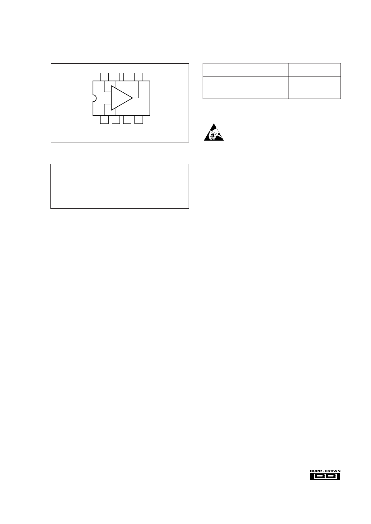
PIN CONFIGURATION
Top View DIP
SO-8
–V
S
7
+V
S
6
–In
8
V
OUT
5
VCA610
2
GND
31
+In
4
Gain
Control,
V
C
No
Internal
Connection
The information provided herein is believed to be reliable; however, BURR-BROWN assumes no responsibility for inaccuracies or omissions. BURR-BROWN assumes
no responsibility for the use of this information, and all use of such information shall be entirely at the user’s own risk. Prices and specifications are subject to change
without notice. No patent rights or licenses to any of the circuits described herein are implied or granted to any third party. BURR-BROWN does not authorize or warrant
any BURR-BROWN product for use in life support devices and/or systems.
ABSOLUTE MAXIMUM RATINGS
Supply .................................................................................................±7V
Differential Input Voltage...............................................................Total V
S
Input Voltage Range ..................................... See Input Protection Section
Storage Temperature Range .......................................... –65°C to +150°C
Lead Temperature (soldering, DIP, 10s)........................................+300°C
Lead Temperature (soldering, SO-8, 3s) ....................................... +260°C
Output Short-Circuit to Ground (+25°C)...................................Continuous
Junction Temperature (T
J
) ............................................................. +175°C
PACKAGE/ORDERING INFORMATION
PACKAGE DRAWING
PRODUCT PACKAGE NUMBER
(1)
VCA610PA 8-Pin Plastic DIP 006
VCA610P 8-Pin Plastic DIP 006
VCA610UA SO-8 Surface-Mount 182
VCA610U SO-8 Surface-Mount 182
NOTE:(1) For detailed drawing and dimension table, please see end of data
sheet, or Appendix C of Burr-Brown IC Data Book.
ELECTROSTATIC
DISCHARGE SENSITIVITY
This integrated circuit can be damaged by ESD. Burr-Brown
recommends that all integrated circuits be handled with
appropriate precautions. Failure to observe proper handling
and installation procedures can cause damage.
ESD damage can range from subtle performance degradation to complete device failure. Precision integrated circuits
may be more susceptible to damage because very small
parametric changes could cause the device not to meet its
published specifications.
Page 4
®
VCA610
4
NOISE FIGURE vs SOURCE RESISTANCE
Source Resistance (Ω)
NF (dB)
25
20
15
10
5
0
10 100 1k 10k 100k
NFdB = 10 log 1 +
e
n
2
+ (inRS)
2
4kTR
S
VOLTAGE AND CURRENT NOISE
vs GAIN
Gain (dB)
10k
1k
100
10
1
–40 –20 0 +20 +40
Voltage Noise (nV/√Hz)
1k
100
10
1
0.1
Current Noise (pA/√Hz)
Output Voltage Noise
Input Current Noise
Input-Referred Voltage Noise
GAIN CONTROL RESPONSE
Frequency (Hz)
Normalized Response (dB)
3
0
–3
–6
–9
–12
–15
10k 100k 1M 10M 100M
GAIN vs CONTROL VOLTAGE
Control Voltage, V
C
(V)
Gain (dB)
60
40
20
0
–20
–40
–60
–80
0.5 0 –0.5 –1 –1.5 –2 –2.5
Output Disabled for
+0.1V ≤ V
C
≤ +2V
Specified Operating Range
SMALL-SIGNAL RESPONSE vs GAIN
Frequency (MHz)
0.1 1.0 10 100
Gain (dB)
50
40
30
20
10
0
–10
–20
–30
–40
–50
VC = –2.0V
VC = –1.5V
VC = –1.0V
VC = –0.5V
V
C
= 0V
Large Signal, VO = 1Vp-p
TYPICAL PERFORMANCE CURVES
At VS = ±5V, RL = 500Ω, RS = 0Ω, and TA = +25°C, unless otherwise noted.
FEEDTHRU WITH OUTPUT DISABLED
Frequency (MHz)
Disabled Gain (dB)
0
–20
–40
–60
–80
–100
0.1 1 10 100
Output Disabled for
+0.1V ≤ V
C
≤ +2V
Page 5

®
VCA610
5
PSR and CMR vs FREQUENCY
Frequency (Hz)
Rejection (dB)
60
50
40
30
20
10
0
10k 100k 1M 10M 100M
–PSR
+PSR
CMR
G = 0dB
OUTPUT OFFSET CHANGE vs GAIN
Gain (dB)
Output Offset Change (mV)
150
100
50
0
–50
–100
–150
–40 –20 0 20 40
Change from Output Offset at G = –40dB
Specification
Limit
Low Grade
High Grade
2-TONE, 3rd ORDER INTERMODULATION
INTERCEPT vs GAIN
Gain (dB)
Intercept Point (dBm)
20
10
0
–10
–20
–30
–40
–40 –20 0 20 40
10MHz1MHz
GROUP DELAY vs GAIN
Gain (dB)
Group Delay (ns)
16
14
12
10
8
6
–40 –20 0 20 40
1MHz
10MHz
15MHz
02550
“DIAMOND PATTERN” RESPONSE
Time (µs)
0 100 200
LARGE SIGNAL RESPONSE
Time (µs)
TYPICAL PERFORMANCE CURVES (CONT)
Output Voltage (mV)
Output Voltage (mV)
G = +40dB
f = 5MHz
R
L
= 500Ω
+500
0
–500
0
At V
S
= ±5V, RL = 500Ω, RS = 0Ω, and TA = +25°C, unless otherwise noted.
–500
+500
Page 6

®
VCA610
6
APPLICATIONS INFORMATION
CIRCUIT DESCRIPTION
The VCA610 is a wideband voltage amplifier with a
voltage-controlled gain, as modeled in Figure 1. The
circuit’s basic voltage amplifier responds to the control
of an internal gain control amplifier. At its input, the
voltage amplifier presents the high impedance of a differential stage, permitting flexible input impedance matching.
To preserve termination options, no internal circuitry
connects to the input bases of this differential stage. For
this reason, the user should provide DC paths for the
input base currents either through a grounded termination resistor or a direct connection to ground. The differential input stage also permits rejection of commonmode signals to remove ground bounce effects. At its
output, the voltage amplifier presents the low impedance
of class A-B emitter-follower stage, again simplifying
impedance matching. An open-loop design produces wide
bandwidth at all gain levels and avoids the added overload-recovery and propagation delays of feedback designs. Repeated use of differential stages minimizes offset effects for reduced feedthrough of the gain control
signal. A ground-sensing, differential to single-ended
converter retains the low offset in the amplifier output
stage.
to +40dB range as V
C
varies from 0 to –2V. Optionally,
making V
C
slightly positive, ≥ 0.1V, effectively disables the
amplifier, giving 80dB of attenuation at low frequencies.
Internally, the gain control circuit varies the amplifier gain
through a time-proven method which exploits the linear
relationship between the transconductance, g
m
, of a bipolar
transistor and the transistor’s bias current. Varying the bias
currents of differential stages varies gm to control the voltage
gain of the VCA610. Relying on transistor g
m
to set gain also
avoids the need for a noise-producing gain-set resistor in the
amplifier input circuit. This reliance normally introduces a
high thermal sensitivity to the gain. However, the VCA610
employs specialized analog signal processing that removes
this thermal effect.
INPUT/OUTPUT RANGE
The VCA610’s 80dB gain range allows the user to handle an
exceptionally wide range of input signal levels. If the unit’s
input and output voltage range specifications are exceeded,
however, signal distortion and amplifier overloading will
occur. The VCA610’s maximum input and output voltage
range is best illustrated in Figure 2.
Gain Control
Circuit
Voltage
Amplifier
Gain Control
Amplifier
V
O
V–GNDV+
–In
+In
V
C
FIGURE 1. Block Diagram of the VCA610.
A user-applied voltage, V
C
, controls the amplifier’s gain
magnitude through a high-speed control circuit. Gain polarity can be either inverting or noninverting depending upon
the amplifier input driven by the input signal. Use of the
inverting input is recommended since this connection tends
to minimize positive feedback from the output to the noninverting input. The gain control circuit presents the high
input impedance of a noninverting op amp connection.
Control voltage V
C
varies the amplifier gain according to the
exponential relationship G(V/V) = 10
–2 (Vc +1)
. This translates to the linear, logarithmic relationship G(dB) = – 40 –
40VC. Thus, G(dB) varies linearly over the specified –40dB
Figure 2 plots output power vs input power for five voltage
gains spaced at 20dB intervals. The 1dBm compression
points occur where the actual output power (solid lines)
deviates by –1dBm from the ideal output power (dashed
lines). Compression is produced by different mechanisms
depending on the selected gain. For example, at G = –40dB,
1dBm compression occurs when the input signal approaches
approximately 3Vp-p (13.5dBm for R
S
= 50Ω). Input over-
loading is the compression mechanism for all gains from
–40dB to about –5dB. For gains between –5dB and +5dB,
the compression is due to internal gain stage overloading.
Compression over this gain range occurs when the output
signal becomes distorted as internal gain stages become
overdriven. At G = 0dB, 1dBm compression occurs when
the input exceeds approximately 1.5Vp-p (7.5dBm). At
gains greater than about 5dB, the compression mechanism is
due to output stage overloading. Output overloading occurs
FIGURE 2. Input and Output Range.
OUTPUT POWER vs INPUT POWER
Input Power in dBm
(
Differential Input Voltage in Vp-p
)
+10
0
–10
–20
–30
–40
–50
–60
–60
(6E-4)
Output Power (dBm)
6.33
V
OUT
(Vp-p)
–50
(0.002)
–40
(0.006)
–30
(0.02)
–20
(0.063)
–10
(0.2)0(0.63)
+10
(2)
+20
(6.3)
3.0
2.0
0.633
0.20
0.063
0.02
6E-3
2E-3
G = –40dB
G = –20dB
G = 0dB
G = +20dB
G = +40dB
–1dBm,
Compression
Points
Ideal
—
Actual
+
+
+
+
+
+13.5dBm
(3Vp-p)
Rs = 50Ω
R
L
= 500Ω
f = 1MHz
Page 7

®
VCA610
7
when either the maximum output voltage swing or output
current is exceeded. The VCA610’s high output current of
±80mA insures that virtually all output overloads will be
limited by voltage swing rather than by current limiting. At
G = +40dB, 1dBm compression occurs when the output
voltage approaches 3Vp-p (3.5dBm for R
L
= 500Ω). Table
I below summarizes these results.
one selected gain. Selecting the maximum gain optimizes
offset performance for higher gains where high amplification of the offset effects produces the greatest output offset.
Two features minimize the offset control circuit’s noise
contribution to the amplifier input circuit. First, making the
resistance of R
2
a low value minimizes the noise directly
introduced by the control circuit. This reduces both the
thermal noise of the resistor and the noise produced by the
resistor with the amplifier’s input noise current. A second
noise reduction results from capacitive bypass of the potentiometer output. This filters out power supply noise that
would otherwise couple to the amplifier input.
This filtering action would diminish as the wiper position
approaches either end of the potentiometer but practical
conditions prevent such settings. Over its full adjustment
range, the offset control circuit produces a ±5mV offset
correction for the values shown. However, the VCA610 only
requires one tenth of this range for offset correction, assuring that the potentiometer wiper will always be near the
potentiometer center. With this setting, the resistance seen at
the wiper remains high and this stabilizes the filtering
function.
GAIN CONTROL
The VCA610’s gain is controlled by means of a unipolar
negative voltage applied between ground and the gain control input, pin 3. If use of the output disable feature is
required, a ground-referenced bipolar voltage is needed.
Output disable occurs for +0.1V ≤ V
C
≤ +2V, and produces
80dB of attenuation. The control voltage should be limited
to +2V in disable mode, and –2V in the gain mode in order
to prevent saturation of internal circuitry.
FIGURE 3. Optional Offset Adjustment and Control Line
Filtering.
3a) Optional Offset Adjustment.
3b) Control Line Filtering.
VCA610
1µF
V
C
V–
V
IN
V
O
R
V
100kΩ
R
2
10Ω
V+
R
1
10kΩ
VCA610
V
O
R
P
Cp
f
–3dB
=
1
2π Rp Cp
V
C
WIRING PRECAUTIONS
Maximizing the VCA610’s capability requires some wiring
precautions and high-frequency layout techniques. In general, printed circuit board conductors should be as short and
as wide as possible to provide low resistance, low impedance signal paths. Stray signal coupling from the output or
power supplies to the inputs should be minimized. Unused
inputs should be grounded as close to the package as
possible.
Low impedance ground returns for signal and power are
essential. Proper supply bypassing is also extremely critical
and must always be used. Both power supply leads should be
bypassed to ground as close as possible to the amplifier pins.
Tantalum capacitors (1µF to 10µF) with very short leads are
recommended. Surface mount bypass capacitors will provide excellent results due to their low lead inductance.
OVERLOAD RECOVERY
As shown in Figure 2, the onset of overload occurs whenever the actual output begins to deviate from the ideal
expected output. If possible, the user should operate the
VCA610 within the linear regions shown in order to minimize signal distortion and overload delay time. However,
instances of amplifier overload are actually quite common in
Automatic Gain Control (AGC) circuits which involve the
application of variable gain to signals of varying levels. The
VCA610’s design incorporates circuitry which allows it to
recover from most overload conditions in 200ns or less.
Overload recovery time is defined as the time required for
the output to return from overload to linear operation following the removal of either an input or gain control overdrive
signal.
OFFSET ADJUSTMENT
Where desired, the offset of the VCA610 can be removed as
shown in Figure 3. This circuit simply presents a DC voltage
to one of the amplifier’s inputs to counteract the offset error
voltage. For best offset performance, the trim adjustment
should be made with the amplifier set at the maximum gain
of the intended application. The offset voltage of the VCA610
varies with gain, limiting the complete offset cancellation to
OUTPUT COMPRESSION TO PREVENT
GAIN RANGE MECHANISM OPERATE WITHIN
–40dB < G < –5dB Input Stage Overload Input Voltage Range
–5dB < G < +5dB Internal Stages Overloading Output Voltage Range
+5dB < G < +40dB Output Stage Overload Output Voltage Range
TABLE I. Output Signal Compression.
Page 8

®
VCA610
8
The VCA610’s gain control input has a –3dB bandwidth of
1MHz and varies with frequency as shown in the Typical
Performance Curves. This wide bandwidth, although useful
for many applications, can allow high frequency noise to
modulate the gain control input. In practice, this can be
easily avoided by filtering the control input as shown in
Figure 3b. R
P
should be no greater than 100Ω so as not to
introduce gain errors by interacting with the gain control’s
input bias current of 2µA.
INPUT PROTECTION
Electrostatic damage (ESD) has been well recognized for
MOSFET devices, but any semiconductor device deserves
protection from this potentially damaging source. The
VCA610 incorporates on-chip ESD protection diodes as
shown in Figure 4. This eliminates the need for the user to
add external protection diodes, which can add capacitance
and degrade AC performance.
ULTRASOUND TGC AMPLIFIER
The Figure 5 block diagram illustrates the fundamental
configuration common to pulse-echo imaging systems. A
piezoelectric crystal serves as both the ultrasonic pulse
generator and the echo monitor transducer. A transmit/
receive (T/R) switch isolates the monitor amplifier from the
crystal during the pulse generation cycle and, then, connects
the amplifier to the crystal during the echo monitor cycle.
FIGURE 4. Internal ESD Protection.
External
Pin
+V
S
–V
S
Internal
Circuitry
ESD Protection diodes internally
connected to all pins.
All pins on the VCA610 are internally protected from ESD
by means of a pair of back-to-back reverse-biased diodes to
either power supply as shown. These diodes will begin to
conduct when the pin voltage exceeds either power supply
by about 0.7V. This situation can occur with loss of the
amplifier’s power supplies while a signal source is still
present. The diodes can typically withstand a continuous
current of 30mA without destruction. To insure long term
reliability, however, diode current should be externally limited to 10mA whenever possible.
The internal protection diodes are designed to withstand
2.5kV (using Human Body Model) and provides adequate
ESD protection for most normal handling procedures. However, static protection is strongly recommended since static
damage can cause subtle changes in amplifier operational
characteristics without necessarily destroying the device.
APPLICATIONS
The electronically variable gain of the VCA610 suits pulseecho imaging systems well. Such applications include medical
imaging, non-destructive structural inspection and optical
distance measurement. The amplifier’s variable gain also
serves AGC amplifiers, amplitude-stabilized oscillators,
log amplifiers and exponential amplifiers. The discussions
below present examples of these applications.
FIGURE 5. Typical Ultrasound Application.
VCA610
V
C
Transducer
ADC
& DSP
V
C
t
0
–2V
T/R
Switch
Transmit
Receive
During the monitor (receive) cycle, the control voltage VC,
varies the amplifier gain. The gain is varied for three basic
signal processing requirements of a transducer array based
beamformer: compensation for depth attenuation effects,
sometimes called Time Gain Compensation (TGC); receive
apodization or windowing for reducing side lobe energy;
and dynamic aperture sizing for better near field resolution.
Time gain compensation increases the amplifier’s gain as
the ultrasound signal moves through the material to compensate for signal attenuation versus material depth. For this
purpose, a ramp signal applied to the VCA610 gain control
input linearly increases the dB gain of the VCA610 with
time. The gain control provides signal apodization or
windowing with transducer arrays connected to amplifier
arrays. Selective weighting of amplifier gains across the
transducer aperture suppresses side lobe effects in the
beamformer output to reduce image artifacts. Gain controlled attenuation or disabling the amplifier can be used to
dynamically size the array aperture for better near field
resolution. The controlled attenuation of the VCA610 minimizes switching artifacts and eliminates the bright radial
rings that can result. The VCA610’s 80dB gain range accommodates these functions.
WIDE-RANGE LOW-NOISE VCA
Figure 6 combines two VCA610s in series, extending the
overall gain range and improving noise performance. This
combination produces a gain equal to the sum of the two
amplifier’s logarithmic gains for a composite range of
Page 9

®
VCA610
9
–80dB to +80dB. Simply connecting V
C1
and VC2 to the
same 0 to –2V gain control voltage can produce this range,
however, separate control voltages for the two amplifiers
offer a noise performance improvement. In that configuration, each amplifier separately controls one half the gain
range in a manner that always holds G
1
at the maximum
level possible.
FIGURE 6. Two Series Connected VCA610s Expand the
Gain Range and Improve Noise Performance.
GAIN
–80dB to 0dB 0dB to 80dB
V
C1
0 to –2V –2V
G
1
–40dB to +40dB +40dB
V
C2
0V 0 to –2V
G
2
–40dB –40dB to +40dB
G
2
G
1
V
C2
V
O
V
C1
V
IN
VCA
1
VCA
2
At higher gains, variation of VC2 alone makes VCA2 provide
all of the gain control, leaving the gain of VCA
1
fixed at its
maximum of 40dB. This gain maximum corresponds to the
maximum bias currents in VCA1, minimizing this amplifier’s
noise. Thus, for composite circuit gains of 0dB to +80dB,
V
CA1
serves as a low-noise, fixed-gain preamp.
For lower composite gains, VCA
1
provides the gain control
and VCA
2
acts as a fixed attenuator. There, variation of V
C1
varies G1 from –40dB to +40dB while VC2 remains fixed at
0V for G
2
= –40dB. This mode produces the –80dB to 0dB
segment of the composite gain range.
FIGURE 8. Adding Wein-bridge Feedback to the AGC Circuit of Figure 7 Produces an Amplitude Stabilized Oscillator.
VCA610
C
H
1µF
V–
OPA620
V
R
0.1 VDC
V
OPEAK
= V
R
V
O
R
3
HP5082
R
1
50kΩ
C
W1
4700pF
R
4
100Ω
1kΩ
R
2
50kΩ
R
W1
300Ω
R
W2
300Ω
C
W2
4700pF
C
C
10pF
f = 1/2πR
W1CW1
V
C
R
W1 = RW2
C
W1 = CW2
WIDE-RANGE AGC AMPLIFIER
The voltage-controlled gain feature of the VCA610 makes
this amplifier ideal for precision AGC applications with
control ranges as large as 60dB. The AGC circuit of Figure
7 adds an op amp and diode for amplitude detection, a
holding capacitor to store the control voltage and resistors
R
1
through R3 that determine attack and release times.
Resistor R
4
and capacitor CC phase compensate the AGC
feedback loop. The op amp compares the positive peaks of
output VO with a DC reference voltage VR. Whenever a V
O
peak exceeds VR, the OPA620 output swings positive, forward biasing the diode and charging the holding capacitor.
This drives the capacitor voltage in a positive direction,
reducing the amplifier gain. R
3
and the CH largely determine
the attack time of this AGC correction.
Between gain corrections, resistor R
1
charges the capacitor
in a negative direction, increasing the amplifier gain. R
1
, R
2
and CH determine the release time of this action. Resistor R
2
forms a voltage divider with R1, limiting the maximum
negative voltage developed on C
H
. This limit prevents input
overload of the VCA610’s gain control circuit.
FIGURE 7. This AGC Circuit Maintains a Constant Output
Amplitude for a 1000:1 Input Range.
VCA610
C
H
0.1µF
V–
V
IN
OPA620
V
R
V
OUT PEAK
= V
R
V
O
R
3
1kΩ
HP5082
R
1
50kΩ
2mV to 2V
100kHz
R
2
50kΩ
C
C
50pF
0.1 VDC
R
4
100Ω
V
C
Page 10

®
VCA610
10
STABILIZED WEIN-BRIDGE OSCILLATOR
Adding Wein-bridge feedback to the above AGC amplifier
produces an amplitude-stabilized oscillator. Shown in
Figure 8, this alternative requires the addition of just two
resistors (R
W1
, RW2) and two capacitors (CW1, CW2).
Connecting the feedback network to the amplifier’s
noninverting input introduces positive feedback to induce
oscillation. The feedback factor displays a frequency dependence due to the changing impedances of the C
W
capacitors.
As frequency increases, the decreasing impedance of the
CW2 increases the feedback factor. Simultaneously, the decreasing impedance of the C
W1
decreases this factor.
Analysis shows that the maximum factor occurs at f =
1/2πR
WCW
, making this the frequency most conducive to
oscillation. At this frequency the impedance magnitude of
CW equals RW and inspection of the circuit shows that this
condition produces a feedback factor of 1/3. Thus, selfsustaining oscillation requires a gain of three through the
amplifier. The AGC circuitry establishes this gain level.
Following initial circuit turn on, R1 begins charging C
H
negative, increasing the amplifier gain from its minimum.
When this gain reaches three, oscillation begins at f =
1/2πRWCW and R1’s continued charging effect makes the
oscillation amplitude grow. This growth continues until that
amplitude reaches a peak value equal to VR. Then, the AGC
circuit counteracts the R
1
effect, controlling the peak ampli-
tude at V
R
by holding the amplifier gain at a level of three.
Making V
R
an AC signal, rather than a DC reference,
produces amplitude modulation of the oscillator output.
LOW-DRIFT WIDEBAND LOG AMP
The VCA610 can be used to provide a 250kHz (–3dB) log
amp with low offset voltage and low gain drift.
The exponential gain control characteristic of the VCA610
permits simple generation of a temperature-compensated
logarithmic response. Enclosing the exponential function in
an op amp feedback path inverts this function, producing the
log response. Figure 9 shows the practical implementation
of this technique. A DC reference voltage, V
R
, sets the
VCA610 inverting input voltage. This makes the amplifier’s
output voltage VOA = – GVR where G = 10
-2 (Vc + 1)
.
A second input voltage also influences V
OA
through control
of gain G. The feedback op amp forces V
OA
to equal the
input voltage V
IN
connected at the op amp inverting input.
Any difference between these two signals drops across R
3
,
producing a feedback current that charges C
C
. The resulting
change in V
OL
adjusts the gain of the VCA610 to change
V
OA
. At equilibrium, VOA = VIN = –VR10
-2 (Vc +1)
. The op
amp forces this equality by supplying the gain control
voltage VC = R1 V
OL
/(R1 + R2). Combining the last two
expressions and solving for V
OL
yields the circuit’s logarith-
mic response.
V
OL
= – (1 + R2/R1) [1 + 0.5LOG (–V
IN /VR
)]
Examination of this result illustrates several circuit characteristics. First, the argument of the Log term, –V
IN/VR
,
reveals an option and a constraint. In Figure 9, V
R
represents
a DC reference voltage. Optionally, making this voltage a
second signal produces log-ratio operation. Either way, the
Log term’s argument constrains the polarities of V
R
and VIN.
These two voltages must be of opposite polarities to ensure
a positive argument. This polarity combination results when
V
R
connects to the inverting input of the VCA610. Alter-
nately, switching V
R
to this amplifier’s noninverting input
removes the minus sign of the log term’s argument. Then,
both voltages must be of the same polarity to produce a
positive argument. In either case, the positive polarity requirement of the argument restricts VIN to a unipolar range.
The above V
OL
expression reflects a circuit gain introduced
by the presence of R
1
and R2. This feature adds a convenient
scaling control to the circuit. However, a practical matter
sets a minimum level for this gain. The voltage divider
formed by R
1
and R2 attenuates the voltage supplied to the
V
C
terminal by the op amp. This attenuation must be great
enough to prevent any possibility of an overload voltage at
the VC terminal. Such an overload saturates the VCA610’s
gain control circuitry, reducing the amplifier’s gain. For the
feedback connection of Figure 9, this overload condition
permits a circuit latch. To prevent this, choose R
1
and R2 to
ensure that the op amp can not possibly deliver more than
2.5V to the VC terminal.
FIGURE 9. Driving the Gain Control Pin of the VCA610 with
a Feedback Amplifier Produces a TemperatureCompensated Log Response.
R
1
470Ω
VCA610
R
2
330Ω
V
OL
V
R
–10mV
OPA620
V
IN
VOA = –G V
R
C
C
50pF
R
3
100Ω
VOL = – 1 +
1 + 0.5 Log (–VIN/VR)
R
1
R
2
( )
V
C
LOW-DRIFT WIDEBAND EXPONENTIAL AMP
A common use of the Log amp above involves signal
companding. The inverse function, signal expanding, requires an exponential transfer function. The VCA610 produces this latter response directly as shown in Figure 10. DC
reference V
R
again sets the amplifier’s input voltage and the
input signal V
IN
now drives the gain control point. Resistors
R
1
and R2 attenuate this drive to prevent overloading the
gain control input. Setting these resistors at the same values
as in the preceding Log amp produces an exponential amplifier with the inverse function of the Log amp.
Page 11

®
VCA610
11
FIGURE 10. Signal Drive of the VCA610 Gain Control Pin
Produces and Exponential Response, Re-expanding Signal Companded by Figure 9.
R
2
330Ω
VCA610
R
1
470Ω
V
O
= –VR10
–2 [R1 VIN /(R1 + R2) + 1]
V
IN
V
R
–10mV
V
C
FIGURE 11. This Voltage-Tuneable Low-Pass Filter Pro-
duces a Variable Cutoff Frequency with a
3,000:1 Range.
Finite loop gain and a signal swing limitation set performance boundaries for the circuit. Both limitations occur
when the VCA610 attenuates rather than amplifies the
feedback signal. These two limitations reduce the circuit’s
utility at the lower extreme of the VCA610’s gain range. For
–1 ≤ V
C
≤ 0, this amplifier produces attenuating gains in the
range from 0dB to –40dB. This directly reduces the net gain
in the circuit’s feedback loop, increasing gain error effects.
Also, this attenuation transfers an output swing limitation
from the OPA620 output to the overall circuit’s output. Note
that OPA620 output voltage, V
OA
, relates to VO through the
expression V
O
= GVOA. Thus, a G < 1 limits the maximum
V
O
swing to a value less than the maximum VOA swing.
However, the circuit shown provides greater output swing
than the more common multiplier implementation. The latter
replaces the VCA610 of the figure with an analog multiplier
having a response of V
O
= XY/10. Then, X = VOA and Y =
V
C
, making the circuit output voltage VO = VOAVC/10. Thus,
the multiplier implementation amplifies V
OA
by a gain of VC/
10. Circuit constraints require that V
C
≤ 10, making this gain
≤ 1. Thus, the multiplier performs only as a variable attenuator and never provides amplification. As a result, the
voltage swing limitation of V
OA
restricts the VO swing
throughout most of the circuit’s control range. Replacing the
multiplier with the VCA610 shown permits equivalent gains
greater > 1. Then, operating the VCA610 with gains in the
range of one to 100 avoids the reduction in output swing
capability.
VOLTAGE-CONTROLLED HIGH-PASS FILTER
A circuit analogous to the above low-pass filter produces a
voltage-controlled high-pass response. The gain control provided by the VCA610 of Figure 12 varies this circuit’s
response zero from 1Hz to 10kHz according to the relationship F
Z
≈ 1/2πGR1C where G = 10
–2 (VC + 1)
.
fP = G/2πR2C G = 10
–2(VC + 1)
V
O
V
I
= –
R
2
R
1
1
1 + R
2
Cs/G
VOLTAGE-CONTROLLED LOW-PASS FILTER
In the circuit of Figure 11, the VCA610 serves as the
variable gain element of a voltage-controlled low-pass filter.
As will be described, this implementation expands the circuit’s
voltage swing capability over that normally achieved with
the equivalent multiplier implementation. The circuit’s response pole responds to control voltage V
C
according to the
relationship f
P
= G/2πR2C where G = 10
–2 (VC + 1)
. With the
components shown, the circuit provides a linear variation of
the low-pass cutoff from 300Hz to 1MHz.
FIGURE 12. A Voltage-Tunable High-Pass Filter Pro-
duces a Response Zero Variable from 1Hz to
10kHz.
The response control results from amplification of the feedback voltage applied to R
2
. Consider first the case where the
VCA610 produces G = 1. Then, the circuit performs as if
this amplifier were replaced by a short circuit. Visually
doing so leaves a simple voltage amplifier with a feedback
resistor bypassed by a capacitor. This basic circuit produces
a response pole at f
P
= 1/2πR2C.
For G > 1, the circuit applies a greater voltage to R
2
,
increasing the feedback current this resistor supplies to the
summing junction of the OPA620. The increased feedback
current produces the same result as if R
2
had been decreased
in value in the basic circuit described above. Decreasing the
effective R2 resistance moves the circuit’s pole to a higher
frequency, producing the f
P
= G/2πR2C response control.
OPA620
VCA610
V
C
V
O
V
OA
0.047µF
330Ω
R
2
330Ω
R
1
C
V
I
OPA620
VCA610
V
C
0.047µF
V
OA
CR
3
33Ω
V
O
R
2
33kΩ
R
1
33kΩ
V
I
For R3 << GR1 and f << 1/2πR3Cs,
V
O
V
I
R
2
R
1
(1 + GR1Cs), fZ = 1/2πGR1C
where G = 10
–2(VC + 1)
= –
Page 12

®
VCA610
12
To visualize the circuit’s operation, consider a circuit condition and an approximation that permit replacing the VCA610
and R
3
with short circuits. First consider the case where the
VCA610 produces G = 1. Then, replacing this amplifier with
short circuit leaves the operation unchanged. In this shorted
state, the circuit is simply a voltage amplifier with an R–C
bypass around R1. The resistance of this bypass, R3, serves
only to phase compensate the circuit and practical factors
make R3 << R1. Neglecting R3 for the moment, the circuit
becomes just a voltage amplifier with capacitive bypass of
R1. This circuit produces a response zero at fZ = 1/2πR1C.
Adding the VCA610 as shown permits amplification of the
signal applied to capacitor C and produces voltage control
of the frequency f
Z
. Amplified signal voltage on C increases the signal current conducted by the capacitor to the
op amp feedback network. The result is the same as if C
had been increased in value to GC. Replacing C with this
effective capacitance value produces the circuit’s control
expression f
Z
= 1/2πR1GC.
Two factors limit the high-frequency performance of the
resulting high-pass filter. The finite bandwidth of the op
amp and the circuit’s phase compensation produce response
poles. These limit the frequency duration of the high-pass
response. Selecting the R
3
phase compensation with the
equation R
3
= √(R1/2πfCC) assures stability for all values of
G and sets the circuit’s bandwidth at BW = √(f
C
/2πR1C).
Here, f
C
is the unity-gain crossover frequency of the op amp
used. With the components shown, BW = 100kHz. This
bandwidth provides a high-pass response duration of five
decades of frequency for f
Z
= 1Hz, dropping to one decade
for f
Z
= 10kHz.
The output voltage limit of the VCA610 imposes an input
voltage limit for the filter. The expression V
OA
= GVI relates
these two voltages. Thus, an output voltage limit V
OAL
constrains the input voltage to V
I
≤ V
OAL
/G.
FIGURE 13. Adding the VCA610 to a State-Variable Filter Produces a Voltage-Controlled BandPass Filter With a Center
Frequency Variable Over a 100:1 Range.
VOLTAGE-CONTROLLED BAND-PASS FILTER
The VCA610’s variable gain also provides voltage control
over the center frequency of a band-pass filter. Shown in
Figure 13, this filter follows from the state-variable configuration with the VCA610 replacing the inverter common to
that configuration. Variation of the VCA610 gain moves the
filter’s center frequency through a 100:1 range following the
relationship f
O
= [10
–(VC + 1)
]/2πRC.
As before, variable gain controls a circuit time constant to
vary the filter response. The gain of the VCA610 amplifies
or attenuates the signal driving the lower integrator of the
circuit. This alters the effective resistance of the integrator
time constant producing the response
Evaluation of this response equation reveals a passband gain
of A
O
= –1, a bandwidth of BW = 1/2πnRC and a selectivity
of Q = n10
–(VC + 1)
. Note that variation of control voltage V
C
alters Q but not bandwidth.
The gain provided by the VCA610 restricts the output swing
of the filter. Output signal V
O
must be constrained to a level
that does not drive the VCA610 output, V
OA
, into its saturation limit. Note that these two outputs have voltage swings
related by V
OA
= GVO. Thus, a swing limit V
OAL
imposes a
circuit output limit of V
OL
≤ V
OAL
/G.
–s/nRC
s
2
+ s/nRC + G/R2C
2
V
O
V
I
=
VCA610
OPA620
OPA620
5kΩ
330Ω
nR
R
5kΩ
nR
0.047µF
C
V
C
R
330Ω
V
OA
0.047µF
C
V
I
V
O
V
O
V
I
–s/nRC
s
2
+ s/nRC + G/R2C
2
fO =
10
–(VC + 1)
2πRC
BW =
1
2πnRC
Q = n10
–(VC + 1)
AO = –1
=
 Loading...