

Page 1
PRELIMINARY DATA SHEET
GaAs INTEGRATED CIRCUIT
µµµµ
PG175TA
L-Band PA DRIVER AMPLIFIER
DESCRIPTION
PG175TA is a GaAs MMIC for PA driver amplifier with variable gain function which was developed for PDC
µ
(Personal Digital Cellular in Japan) and another L-band application. The device can operate with 3.0 V, having the
high gain and low distortion.
FEATURES
DD1
• Low Operation Voltage: V
•fRF: 925 to 960 MHz@ P
• Low distortion: P
External input and output matching
• Low operation Current: IDD = 20 mA typ. @ VDD = 3.0 V, P
External input and output matching
• Variable gain control function: ∆G = 35 dB typ. @ V
• 6 pin mini-mold package
out
adj1
= –60 dBc typ. @ VDD = 3.0 V, P
DD2
= V
= +9 dBm
= 3.0 V
out
= +9 dBm, V
out
= +9 dBm, V
AGC
= 0.5 to 2.5 V
AGC
= 2.5 V
AGC
= 2.5 V
APPLICATION
• Digital Cellular: PDC800M, etc.
ORDERING INFORMATION (PLAN)
PART NUMBER PACKAGE PACKING FORM
µ
PG175TA-E3 6 pin Mini-mold Carrier tape width is 8 mm, Quanti ty is 3 kpcs per reel.
Remark
Caution The IC must be handled with care to prevent static discharge because its circuit composed of
For sample order, please contact your local NEC sales office. (Part number for sample order: µPG175TA)
GaAs HJ-FET.
Document No. P13470EJ1V0DS00 (1st edition)
Date Published May 1998 N CP(K)
Printed in Japan
The information in this document is subject to change without notice.
1998©
Page 2
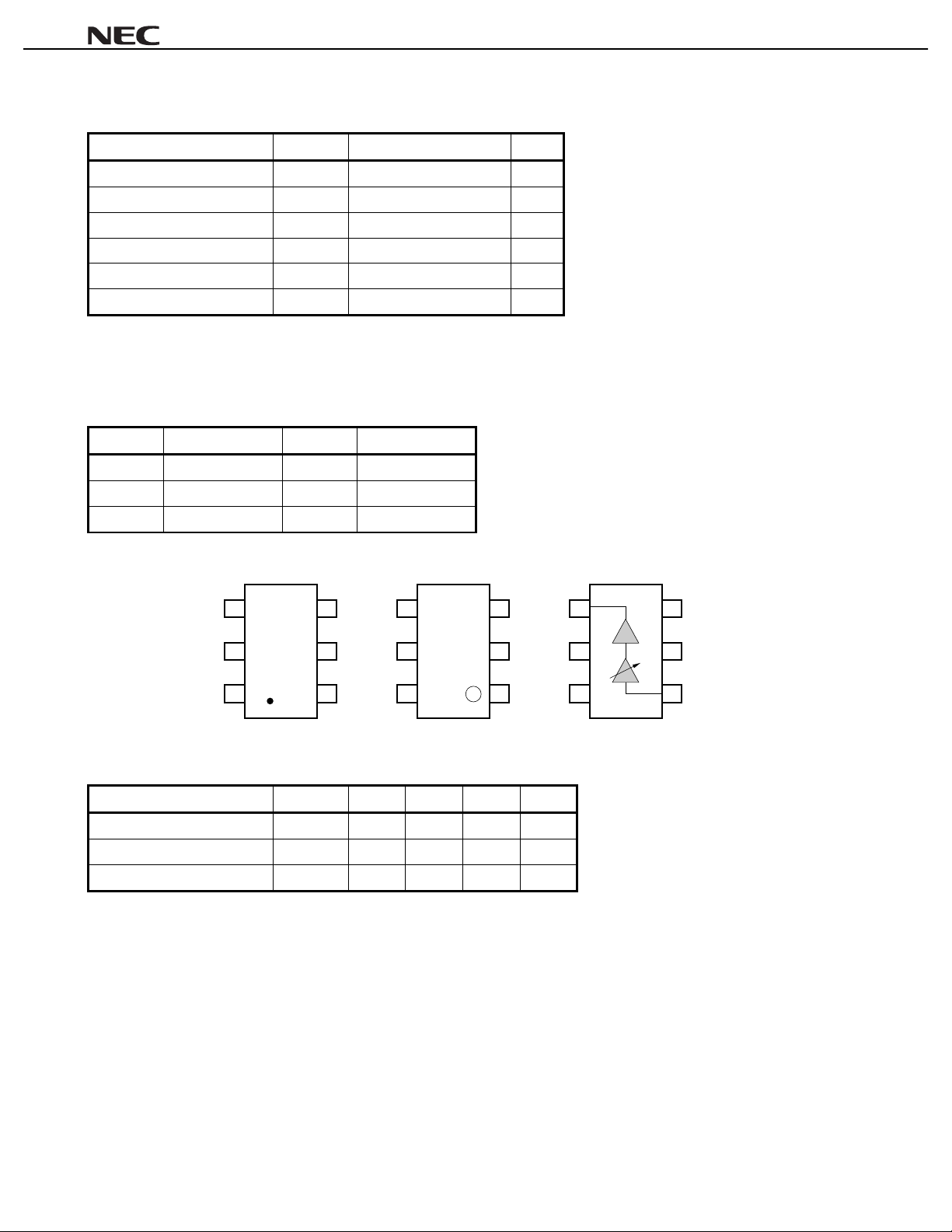
ABSOLUTE MAXIMUM RATINGS (TA = 25°C)
PARAMETERS SYMBOL RATINGS UNIT
DD1
Supply Voltage V
AGC Control Voltage V
Input Power P
Total Power Dissipat i on P
Operating Temperature T
Storage Temperature T
, V
AGC
tot
stg
DD2
in
A
–30 to +90 °C
–35 to +150 °C
6.0 V
6.0 V
–8 dBm
Note
200
mW
µµµµ
PG175TA
Mounted on a 50 × 50 × 1.6 mm double copper clad epoxy glass PWB, T
Note
PIN CONNECTION AND INTERNAL BLOCK DIAGRAM
PIN NO. CONNECTION PIN NO. CONNECTION
1V
DD1
4V
AGC
2 GND 5 GND
3V
DD2
& OUT 6 IN
Top View
3
2
1
4
5
G1E
6
Bottom View
4
5
6
3
2
1
RECOMMENDED OPERATING CONDITIONS (TA = 25°C)
PARAMETERS SYMBOL MIN. TYP. MAX. UNIT
3
2
1
A
= +85°C
Top View
4
5
6
Supply Voltage V
DD1
AGC Control Voltage V
Input Power P
, V
AGC
DD2
+2.7 +3.0 +3.3 V
0.5 2.5 V
in
–21 –17 dBm
Preliminary Data Sheet2
Page 3
µµµµ
PG175TA
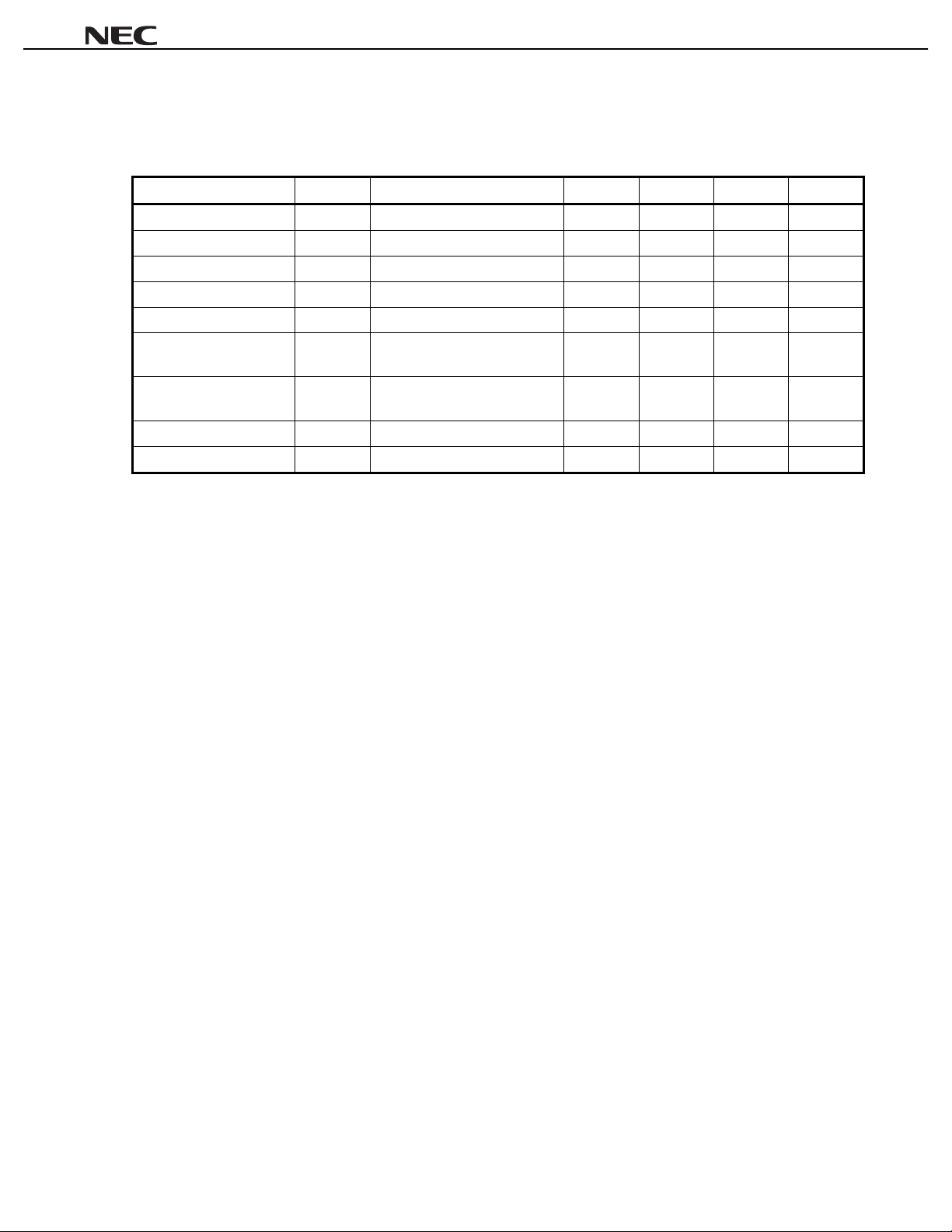
ELECTRICAL CHARACTERISTICS
(Unless otherwise specified, T
A
= 25°C, V
DD1
= V
DD2
= +3.0 V,
/4DQPSK modulated signal input,
ππππ
External input and output matching)
PARAMETERS SYMBOL TEST CONDITIONS MIN. TYP. MAX. UNIT
Operating Frequency f 925 960 MHz
Total Current I
AGC Control Current I
Power Gain G
Variable Gain Range
Adjacent Channel Power
∆
P
Leakage 1
Adjacent Channel Power
P
Leakage 2
Input Return Loss RL
Output Return Loss RL
DD
AGC
adj1
adj2
Pin = –21 dBm, V
AGC
V
= 0.5 to 2.5 V 200 500
p
Pin = –21 dBm, V
G
Pin = –21 dBm, V
out
P
= +9 dBm, V
∆
f = ±50 kHz, 21 kHz Band Width
out
P
= +9 dBm, V
∆
f = ±100 kHz, 21 kHz Band Width
in
External matching 10 dB
out
External matching 10 dB
AGC
= 2.5 V 20 30 mA
AGC
= 2.5 V 27 30 dB
AGC
= 0.5 to 2.5 V
AGC
= 2.5 V
AGC
= 2.5 V
30 35 dB
–60 –55 dBc
–70 –65 dBc
A
µ
Preliminary Data Sheet 3
Page 4

EVALUATION CIRCUIT (Preliminary)
DD1
V
= V
DD2
= +3.0 V, f = 950 MHz
C3
L1
L5
V
DD1
1
G1E
µµµµ
PG175TA
V
DD2
C2
L4
OUT
L3 C1
3
2
456
IN
Using the NEC Evaluation board
C1 2.0 pF
C2, C3 1000 pF
L1 22 nH
L2 27 nH
L3 12 nH
L4 47 nH
L5 10 nH
L2
AGC
V
Preliminary Data Sheet4
Page 5

µµµµ
PG175TA
EVALUATION BOARD (Epoxy Glass,
DD1
V
38 mm
IN
= 4.6, 0.4 mm thickness)
εεεε
L3
C3
L5
L4
L2
L1
40 mm
C2
C1
OUT
DD2
V
V
AGC
6 PIN MINI-MOLD PACKAGE DIMENSIONS (UNIT: mm)
+0.1
0.3
–0.0
123
+0.2
–0.3
+0.2
–0.1
2.8
1.5
654
0.95 0.95
1.9
2.9 ± 0.2
0.13 ± 0.1
0.8
+0.2
1.1
–0.1
0 to 0.1
Preliminary Data Sheet 5
Page 6

µµµµ
PG175TA
RECOMMENDED SOLDERING CONDITIONS
This Product should be soldered in the following recommended conditions. Other soldering methods and
conditions than the recommended conditions are to be consulted with our sales representatives.
Soldering process Soldering conditions
Infrared ray reflow Package peak temperature: 235°C
Hour: within 30 s. (more than 210° C)
Time: 3 times, Limited days: no.
VPS Package peak temperature: 215°C
Hour: within 40 s. (more than 200° C)
Time: 3 times, Limited days: no.
Wave Soldering Soldering tub temperature: les s than 260°C, Hour: within 10 s.
Time: 1 time, Limited days: no.
Pin part heating Pin area tem perature: less than 300°C, Hour: within 3 s.
Limited days: no.
It is the storage days after opening a dry pack, the storage conditions are 25°C, less than 65%, RH.
Note
Note
Note
Note
Note
Recommended condition
symbol
IR35-00-3
VP15-00-3
WS60-00-1
Caution The combined use of soldering method is to be avoided (However, except the pin area heating
method).
For details of recommended soldering conditions for surface mounting, refer to information document
SEMICONDUCTOR DEVICE MOUNTING TECHNOLOGY MANUAL (C10535E).
Preliminary Data Sheet6
Page 7

[MEMO]
µµµµ
PG175TA
Preliminary Data Sheet 7
Page 8

µµµµ
PG175TA
Caution
The Great Care must be taken in dealing with the devices in this guide.
The reason is that the material of the devices is GaAs (Gallium Arsenide), which is
designated as harmful substance according to the law concerned.
Keep the law concerned and so on, especially in case of removal.
The application circuits and their parameters are for reference only and are not intended for use in actual design-ins.
No part of this document may be copied or reproduced in any form or by any means without the prior written
consent of NEC Corporation. NEC Corporation assumes no responsibility for any errors which may appear in this
document.
NEC Corporation does not assume any liability for infringement of patents, copyrights or other intellectual
property rights of third parties by or arising from use of a device described herein or any other liability arising
from use of such device. No license, either express, implied or otherwise, is granted under any patents,
copyrights or other intellectual property rights of NEC Corporation or others.
While NEC Corporation has been making continuous effort to enhance the reliability of its semiconductor devices,
the possibility of defects cannot be eliminated entirely. To minimize risks of damage or injury to persons or
property arising from a defect in an NEC semiconductor device, customers must incorporate sufficient safety
measures in its design, such as redundancy, fire-containment, and anti-failure features.
NEC devices are classified into the following three quality grades:
"Standard", "Special", and "Specific". The Specific quality grade applies only to devices developed based on
a customer designated "quality assurance program" for a specific application. The recommended applications
of a device depend on its quality grade, as indicated below. Customers must check the quality grade of each
device before using it in a particular application.
Standard: Computers, office equipment, communications equipment, test and measurement equipment,
audio and visual equipment, home electronic appliances, machine tools, personal electronic
equipment and industrial robots
Special: Transportation equipment (automobiles, trains, ships, etc.), traffic control systems, anti-disaster
systems, anti-crime systems, safety equipment and medical equipment (not specifically designed
for life support)
Specific: Aircrafts, aerospace equipment, submersible repeaters, nuclear reactor control systems, life
support systems or medical equipment for life support, etc.
The quality grade of NEC devices is "Standard" unless otherwise specified in NEC's Data Sheets or Data Books.
If customers intend to use NEC devices for applications other than those specified for Standard quality grade,
they should contact an NEC sales representative in advance.
Anti-radioactive design is not implemented in this product.
M4 96. 5
 Loading...