

Page 1

PRELIMINARY DATA SHEET
MOS INTEGRATED CIRCUIT
µ
PD9611
FOUR-CHANNEL PCM CODEC
The µPD9611 incorporates 4-channel A-law/µ-law PCM CODECs compliant with ITU-T Recommendation G.711/
G.714 and is suitable for applications such as PBX analog subscriber line circuits.
Its gain setting circuit allows transmit/receive gain to be set for 4 channels independently by externally inputting
digital signals.
FEATURES
Single-chip CMOS monolithic LSI
•
ITU-T Recommendation G.711/G.714 compliant
•
Four-channel PCM CODECs integrated on a single chip
•
Compatible with A-law and µ-law
•
Digital gain setting for each channel
•
• Transmit : +7.5 to –8.0 dB (0.5 dB step)
• Receive : 0 to –15.5 dB (0.5 dB step)
Data transfer system: Transmit/receive synchronization
•
Data rate: 2048 kHz
•
+5 V single power supply
•
Power down function for each channel
•
Low power consumption
•
ORDERING INFORMATION
Part Number Package
µ
PD9611GT 48-pin shrink SOP (375 mil)
The information in this document is subject to change without notice.
Document No. S11018EJ2V0DS00 (2nd edition)
Date Published October 1996 P
Printed in Japan
©
1996
Page 2
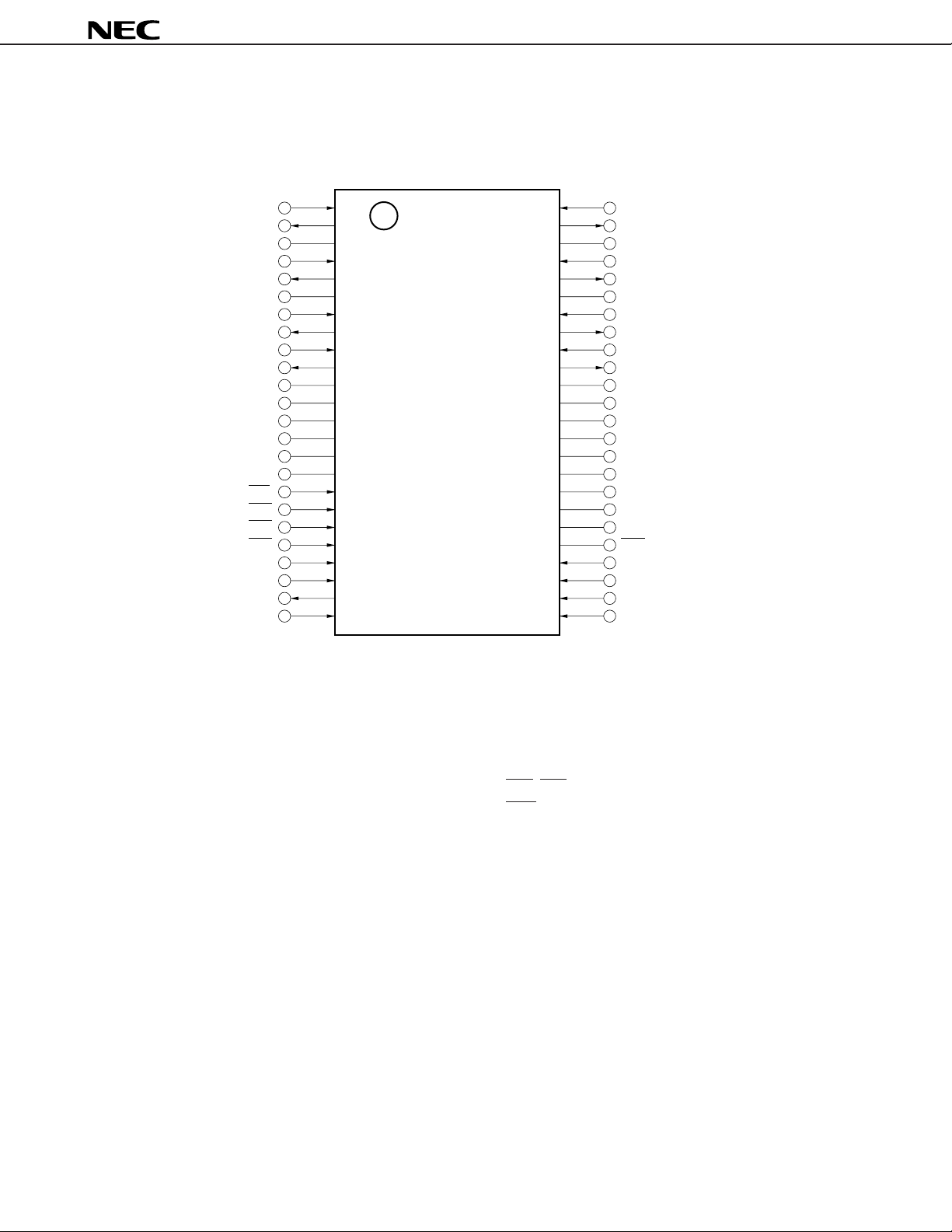
PIN CONFIGURATION (Top View)
48-pin shrink SOP (375 mil)
µ
PD9611
ACOM
ACOM
ACOM
ACOM
A
OUT
A
NC
AIN2
A
OUT
NC
OUT
OUT
AV
DD
AV
DD
AV
DD
AV
DD
DV
NC
PD1
PD2
PD3
PD4
FSC
DCLK
IN
1
1
2
IN
1
1
IN
2
2
1
2
3
4
DD
D
X
D
R
1
2
3
4
5
6
7
8
9
10
11
12
13
14
15
16
17
18
19
20
21
22
23
24
µ
PD9611GT
48
47
46
45
44
43
42
41
40
39
38
37
36
35
34
33
32
31
30
29
28
27
26
25
AIN4
OUT
4
A
NC
IN
3
A
A
OUT
3
NC
ACOM
IN
ACOM
OUT
ACOM
IN
ACOM
OUT
AGND1
AGND2
AGND3
AGND4
SUBGND
DGND
NC
NC
NC
RST
LAW
SP
DATA
SP
SYNC
SP
CLK
3
3
4
4
IN1-ACOMIN4 : Analog common voltage in
ACOM
ACOMOUT1-ACOMOUT4: Analog common voltage out
AGND1-AGND4 : Analog ground
IN1-AIN4 : Analog signal in
A
AOUT1-AOUT4 : Analog signal out
DD1-AVDD4 : Analog power supply
AV
DCLK : Data clock in
DGND : Digital ground
R : Receive PCM data in
D
DVDD : Digital power supply
D
X : Transmit PCM data out
FSC : Frame synchronous clock in
LAW : A-law/µ-law control in
NC : No connection
PD1-PD4 : Power down control
RST : Reset in
CLK : Serial port data clock in
SP
SPDATA : Serial port data in
SPSYNC : Serial port synchronous clock in
SUBGND : Sub ground
2
Page 3
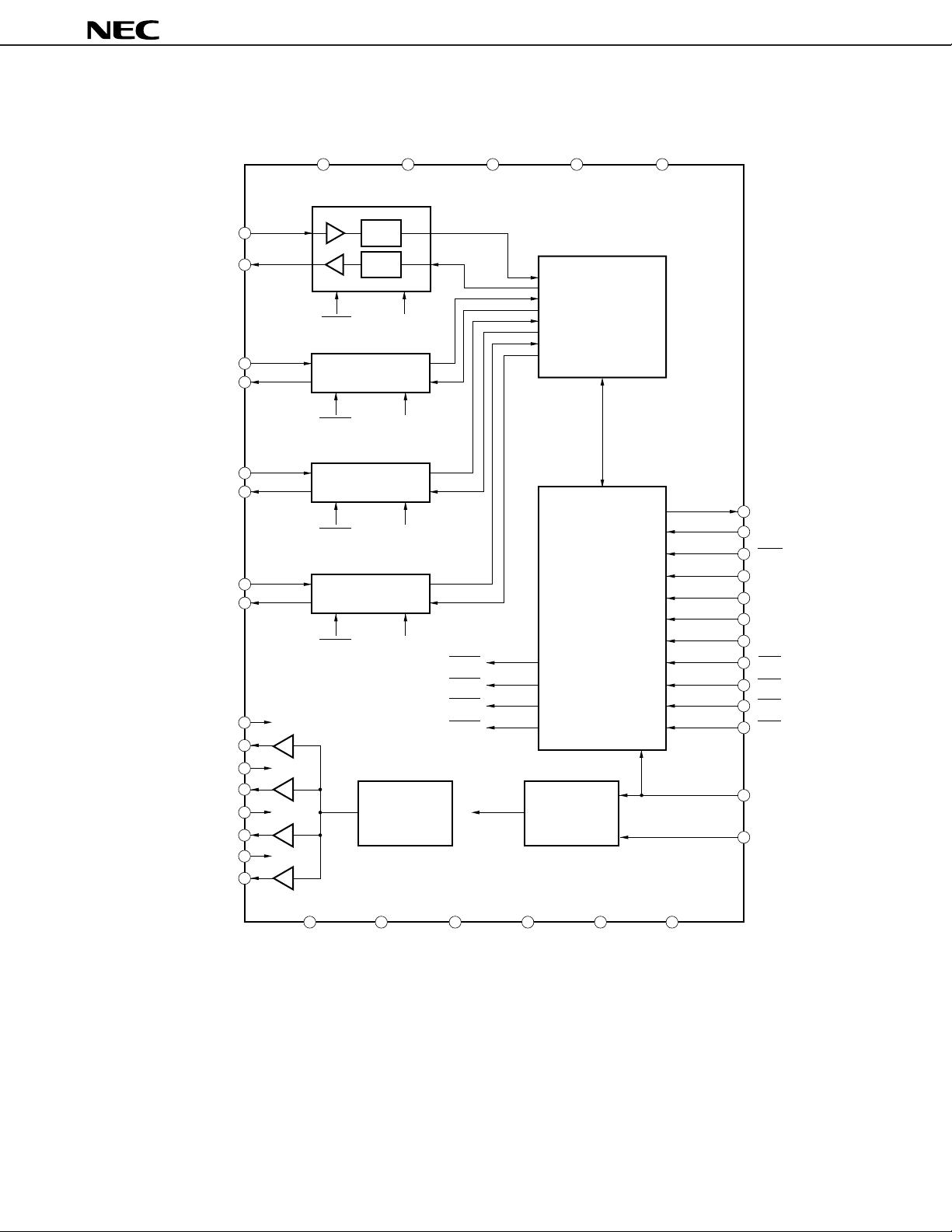
BLOCK DIAGRAM
µ
PD9611
A
A
A
A
ACOMIN1
ACOM
ACOM
ACOM
ACOM
ACOM
ACOM
ACOM
AIN1
OUT
IN
A
OUT
IN
A
OUT
IN
A
OUT
OUT
IN
OUT
IN
OUT
IN
OUT
AVDD1AV
DD
2AV
DD
3AV
DD
4DV
DD
CH1
A/D
1
D/A
DSP
APD1
2
ACOM
CH2
IN
1
Channel FiIter
2
IN
APD2
3
ACOM
CH3
2
3
D
X
D
ACOMIN3APD3
R
RST
SYNC
4
4
CH4
I/O
Linear ↔ A,
µ
DGS
ACOMIN4APD4
MUX, DEMUX
APD1
APD2
APD3
APD4
SP
SP
SP
LAW
PD1
PD2
PD3
PD4
CLK
DATA
1
2
2
3
Voltage
Reference
Clock
Generator
3
FSC
DCLK
4
4
AGND1
AGND2 AGND3 AGND4 DGND SUBGND
3
Page 4
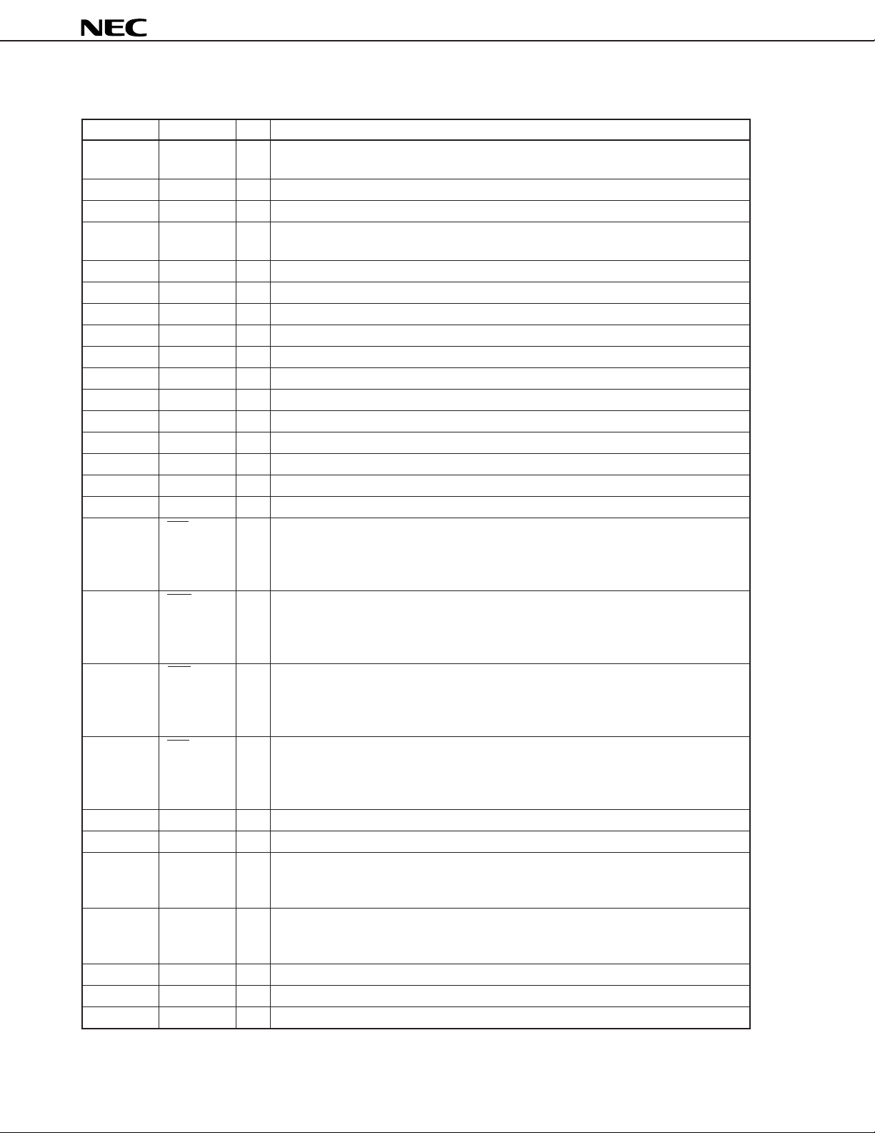
1. PIN DESCRIPTION
Pin No. Symbol I/O Name and Function
1AIN1 I Transmit analog input pin for channel 1
When not used, connect to ACOMOUT1 pin.
2AOUT1 O Receive analog output pin for channel 1
3 NC – Leave this pin open.
4AIN2 I Receive analog input pin for channel 2
When not used, connect to ACOMOUT1 pin.
5AOUT2 O Transmit analog output pin for channel 2
6 NC – Leave this pin open.
7 ACOMIN1 I Signal reference voltage input for channel 1
8 ACOMOUT1 O Signal reference voltage output for channel 1
9 ACOMIN2 I Signal reference voltage input for channel 2
10 ACOMOUT2 O Signal reference voltage output for channel 2
11 AVDD1 – Analog power supply pin for channel 1 +5 ± 0.25 V
12 AVDD2 – Analog power supply pin for channel 2 +5 ± 0.25 V
13 AVDD3 – Analog power supply pin for channel 3 +5 ± 0.25 V
14 AVDD4 – Analog power supply pin for channel 4 +5 ± 0.25 V
15 DVDD – Digital power supply pin +5 ± 0.25 V
16 NC – Leave this pin open.
17 PD1 I Power-down control input pin for channel 1
Channel 1 enters power-down mode when this signal is low level.
The output of DX pin for channel 1 becomes high-impedance and AOUT1 becomes
signal reference voltage in the power-down mode.
18 PD2 I Power-down control input pin for channel 2
Channel 2 enters power-down mode when this signal is low level.
The output of DX pin for channel 2 becomes high-impedance and AOUT2 becomes
signal reference voltage in the power-down mode.
19 PD3 I Power-down control input pin for channel 3
Channel 3 enters power-down mode when this signal is low level.
The output of DX pin for channel 3 becomes high-impedance and AOUT3 becomes
signal reference voltage in the power-down mode.
20 PD4 I Power-down control input pin for channel 4
Channel 4 enters power-down mode when this signal is low level.
The output of DX pin for channel 4 becomes high-impedance and AOUT4 becomes
signal reference voltage in the power-down mode.
21 FSC I Frame synchronous clock input pin (8 kHz)
22 DCLK I Data clock input pin (2048 kHz)
23 DX O Transmit PCM data output pin
This pin outputs PCM data for channel 1 to 4 in synchronization with rising edges
of DCLK after rising edges of FSC. It becomes high-impedance for other timings.
24 DR I Receive PCM data input pin
This pin inputs PCM data for channel 1 to 4 in synchronization with falling edges of
DCLK after rising edges of FSC.
25 SPCLK I Setting data clock input pin
26 SPSYNC I Setting synchronous clock input pin
27 SPDATA I Setting data input pin
µ
PD9611
4
Page 5
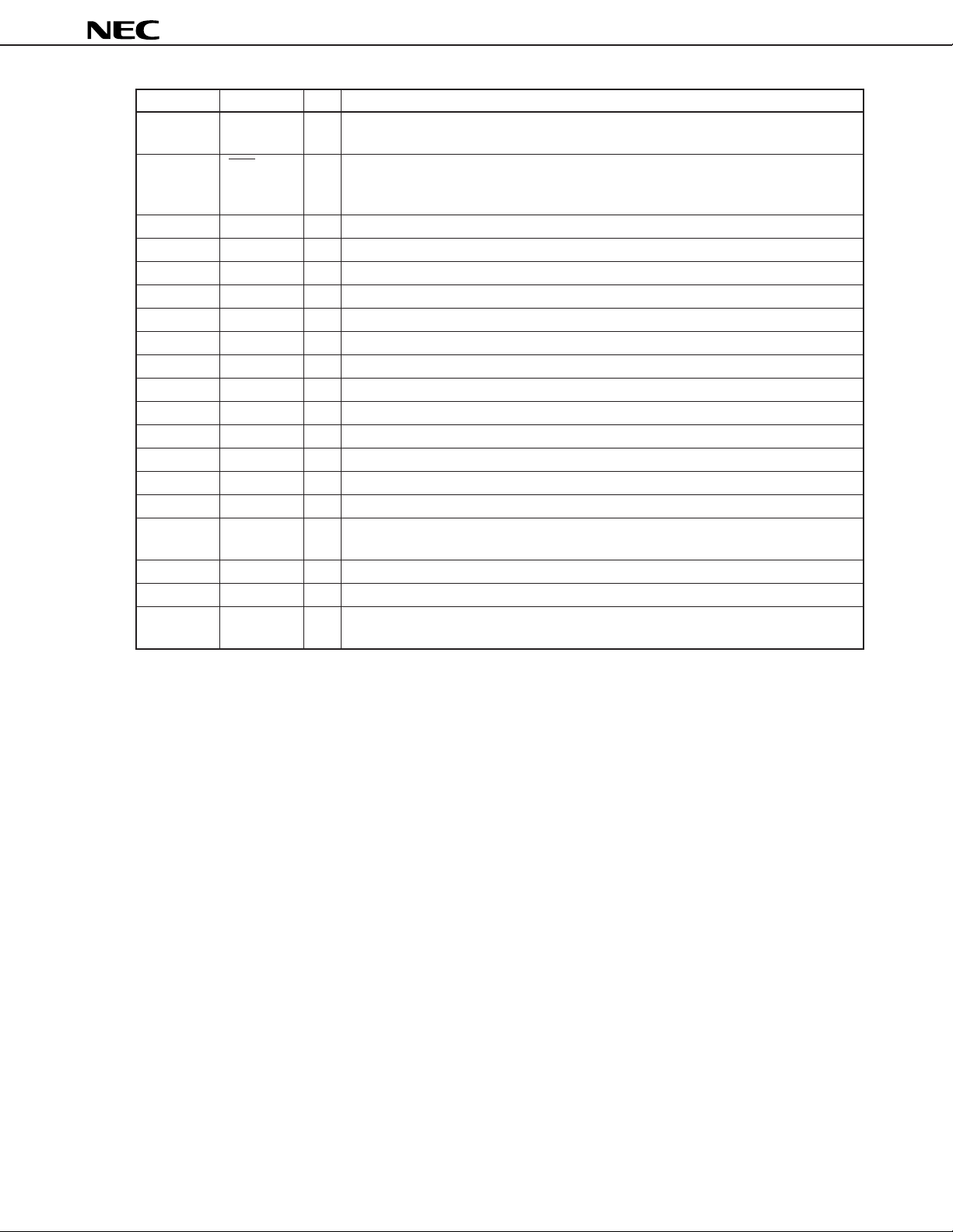
Pin No. Symbol I/O Name and Function
28 LAW I A-law/µ-law select pin in common to four channels
L: A-law, H: µ-law
29 RST – Reset input, power-on reset pin
H: normal operation
L: internal registers are in the default status.
30-32 NC – Leave this pin open.
33 DGND – Digital ground pin
34 SUBGND – Substrate ground pin
35 AGND4 – Analog ground pin for channel 4
36 AGND3 – Analog ground pin for channel 3
37 AGND2 – Analog ground pin for channel 2
38 AGND1 – Analog ground pin for channel 1
39 ACOMOUT4 O Signal reference voltage output for channel 4
40 ACOMIN4 I Signal reference voltage input for channel 4
41 ACOMOUT3 O Signal reference voltage output for channel 3
42 ACOMIN3 I Signal reference voltage input for channel 3
43 NC – Leave this pin open.
44 AOUT3 O Receive analog output pin for channel 3
45 AIN 3 I Transmit analog input pin for channel 3
When not used, connect to ACOMOUT1 pin.
46 NC – Leave this pin open.
47 AOUT4 O Receive analog output pin for channel 4
48 AIN 4 I Transmit analog input pin for channel 4
When not used, connect to ACOMOUT1 pin.
µ
PD9611
5
Page 6
2. CAUTIONS ON USE
(1) Absolute maximum ratings
Application of voltage or current in excess of the absolute maximum ratings to the µPD9611 may result
in damage due to latch up, etc. Be especially cautions about power supply noise, etc.
(2) Wiring pattern
µ
The design of the ground pattern is extremely important for operating the
Connect the analog ground pins (AGND1 to AGND4), digital ground pin (DGND) and substrate ground
pin (SUBGND) close to the IC pins, and connect to a wide analog ground line on the board.
(3) Addition of bypass capacitors for power supply pins
µ
Because the
PD9611 uses many internal high-frequency operational amplifiers, high power supply
impedance can cause instability (such as oscillation) in these internal operational amplifiers. To
suppress such instability and eliminate power supply noise, connect all power supply pins (AV
AVDD4, DVDD) close to the IC pins, and put bypass capacitors (CVDD = approximately 0.1 µF) having
superior high-frequency characteristics very close to the pins.
PD9611 with high precision.
µ
PD9611
DD1 to
(4) Addition of bypass capacitors for ACOM pins
µ
PD9611 incorporates references voltages for signal sources. Superposing of noise on these
The
reference voltages may have adverse effects on transmission characteristics, etc. Therefore, connect
the ACOM
OUT pin and ACOMIN pin close to the IC pins, and put bypass capacitors (CACOM = approximately
0.1 µF) having superior high-frequency characteristics very close to the pins.
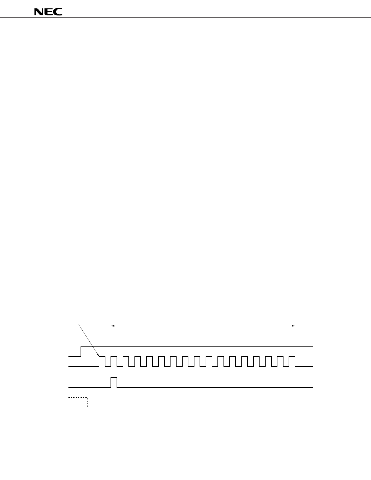
(5) Control or SP
DATA pin on reset
When inputting the setting data from the SPDATA pin after the µPD9611 is reset, first input the following
patterns to reset to 0 the couter used to fetch data from the SPDATA pin.
SP
SP
1 clocks or more
RST
CLK
SYNC
16 clocks or more
SP
DATA
After ther RST pin has been set to the high level, input 1 clock or more to the SPCLK pin, set the SPSYNC
pin to the high level and input 16 clocks more to the SPCLK pin.
During this operation, the SPDATA pin is held at the low level. Afterwards, input the setting data.
6
Page 7
3. GENERAL OPERATION
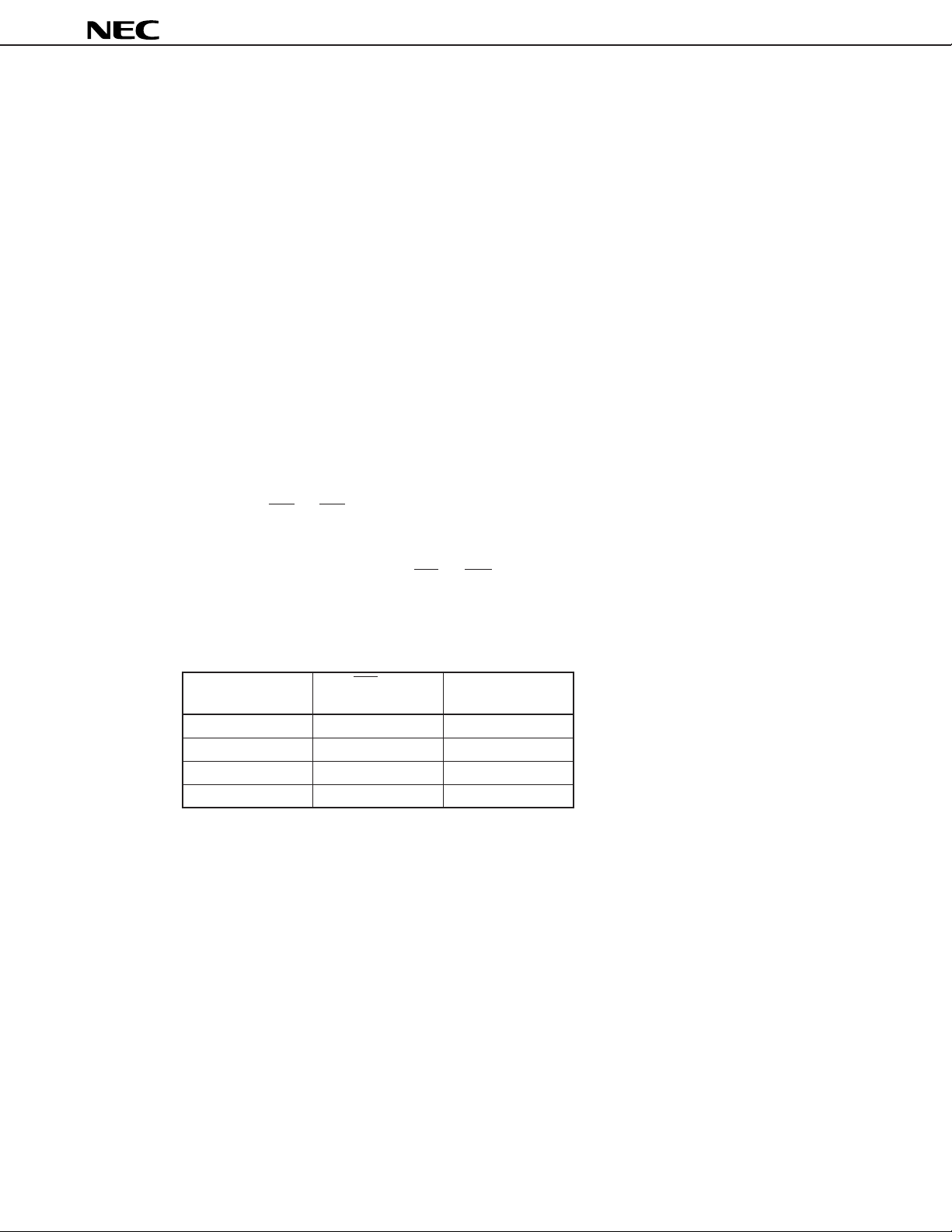
(1) PCM data transfer
In the transmit section, if FSC pin is set to the high level in synchronization with the rising edge (↑) of
the data clock applied to the DCLK pin, the D
1 is output. The following data of 7 bits is clocked out in synchronization with the rising edge (↑) of each
data clock. Sign bit data (MSB) of channel 2 is output in synchronization with the rising edge (↑) of the
9th data clock. In the same manner, each data up to channel 4 is output and the rising edge (↑) of the
33rd data clock then sets the D
Similarly, in the receive section, if the FSC pin is set to the high level in synchronization with the rising
edge (↑) of the data clock applied to the DCLK pin, data of D
the data clock and consecutively clocked in.
(2) Power down control
µ
PD9611 has the following two methods for power down control and is able to control power-down
The
independently for each channel.
X pin becomes active and sign bit data (MSB) of channel
X pin to high-impedance state.
µ
PD9611
R pin is latched by the falling edges (↓) of
• Sets pins PD1 to PD4 to high or low level.
• Inputs 8-bit setting data from SP
DATA pin (see (5) Control of SPDATA pin).
Internal data is the logical sum of PD1 to PD4 pin state and 8-bit setting data input.
If the internal data is 0, the channel enters the power-down state. If the internal data is 1, the channel
enters the power-up state. In the power down state, PCM data in the channel goes to high-impedance
state and analog output becomes the signal reference voltage level.
8-Bit Setting Data PD1 Pin Internal Data
(Channel 1)
000
101
011
111
Remarks 1. 0: Power down, 1: Power up
2. The settings are the same for channel 2 to channel 4.
7
Page 8
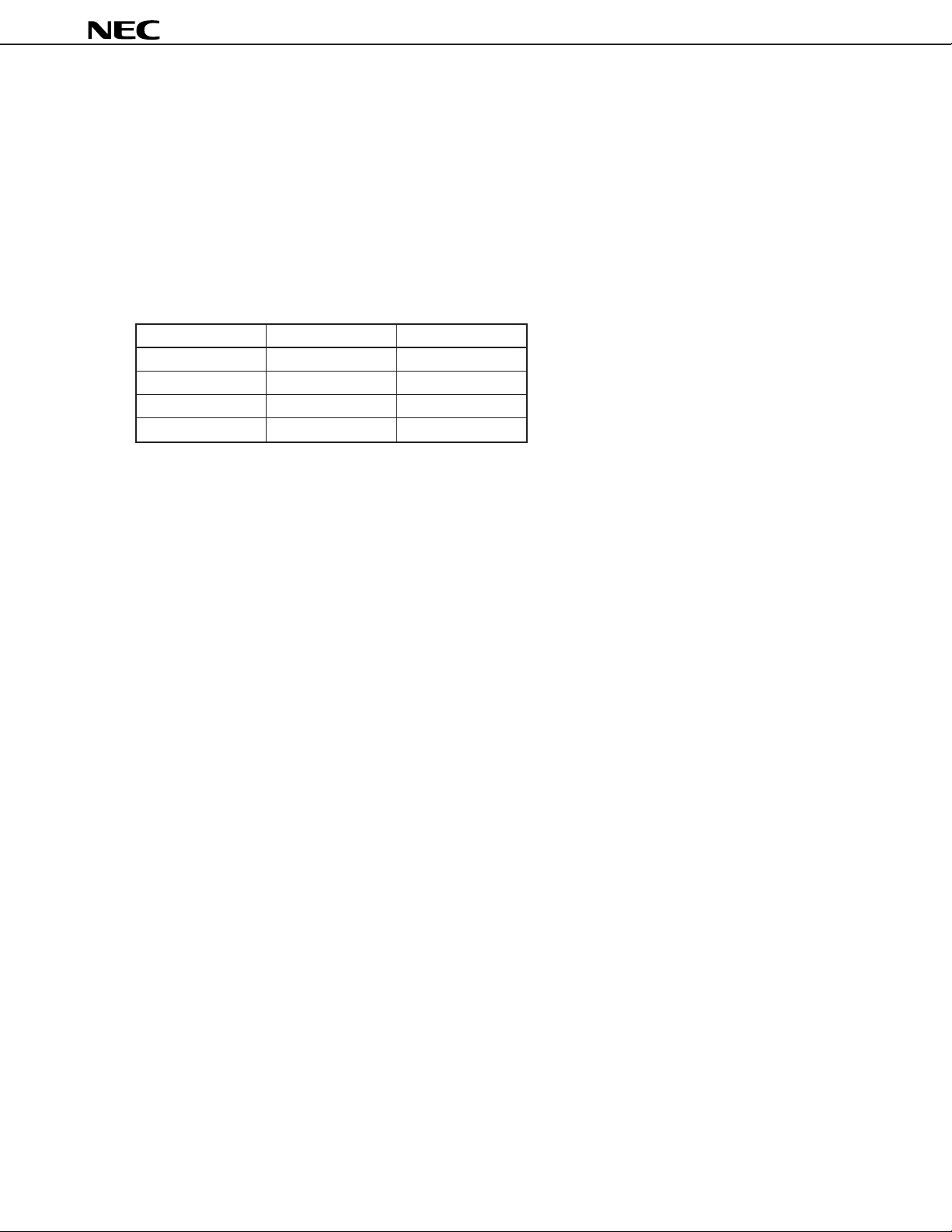
(3) A-law/µ-law control
µ
PD9611 has the following two methods for A-law/µ-law control.
The
• Sets LAW pin to high or low level.
• Inputs 8-bit setting data from SP
Internal data is the logical sum of LAW pin state and 8-bit setting data input.
If the internal data is 0, the
µ
-law mode.
8-Bit Setting Data LAW Pin Internal Data
000
101
011
111
Remark 0: A-law, 1: µ-law
µ
DATA pin (see (5) Control of SPDATA pin).
PD9611 enters A-law mode. If the internal data is 1, the µPD9611 enters
µ
PD9611
(4) Gain Setting control for transmit/receive
µ
PD9611 can control gain settings independently for the transmit/receive by inputting 8-bit setting
The
data (see (5) Control of SPDATA pin) from the SPDATA pin for four channels. Gain can be set from +7.5
to –8.0 dB for the transmit and +0.0 dB t o –15.5 dB for the receive in 0.5 dB steps.
8-bit setting data input from SP
of transmit/receive and gain setting in the second 8 bits.
DATA pin specifies the channel set in the first 8 bits, and performs selection
8
Page 9
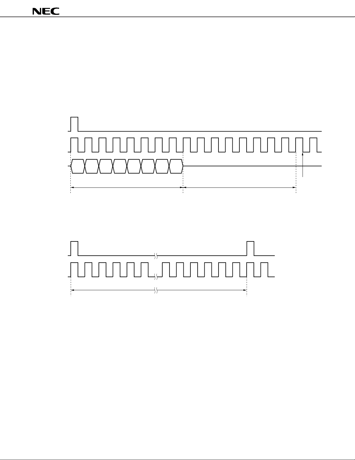
(5) Control of SPDATA pin
SYNC pin is set to the high level in synchronization with the rising edge (↑) of the data clock applied
If SP
to the SPCLK pin, data of the SPDATA pin is latched by the falling edge (↓) of the data clock and
consecutively fetched in.
After the 8-bit data has been fetched, the setting operation is performed according to the data.
This setting operation is performed during the 8 clocks after fetching the data and the next data is valid
at the 17th clock.
Therefore, when setting 1 word (8 bits) of data, input 17 clocks or more to the SP
SP
SYNC
CLK pin.
µ
PD9611
SP
SP
SP
123456789101112131415161718
CLK
DATA
Ensure that 17 clocks or more are input to the SP
SYNC.
17 clocks or more
SP
SYNC
CLK
the next SP
Don’t care
Setting operationData fetch
CLK pin between the rising of SPSYNC and the rising of
Setting
completed
(The next
data is valid.)
9
Page 10
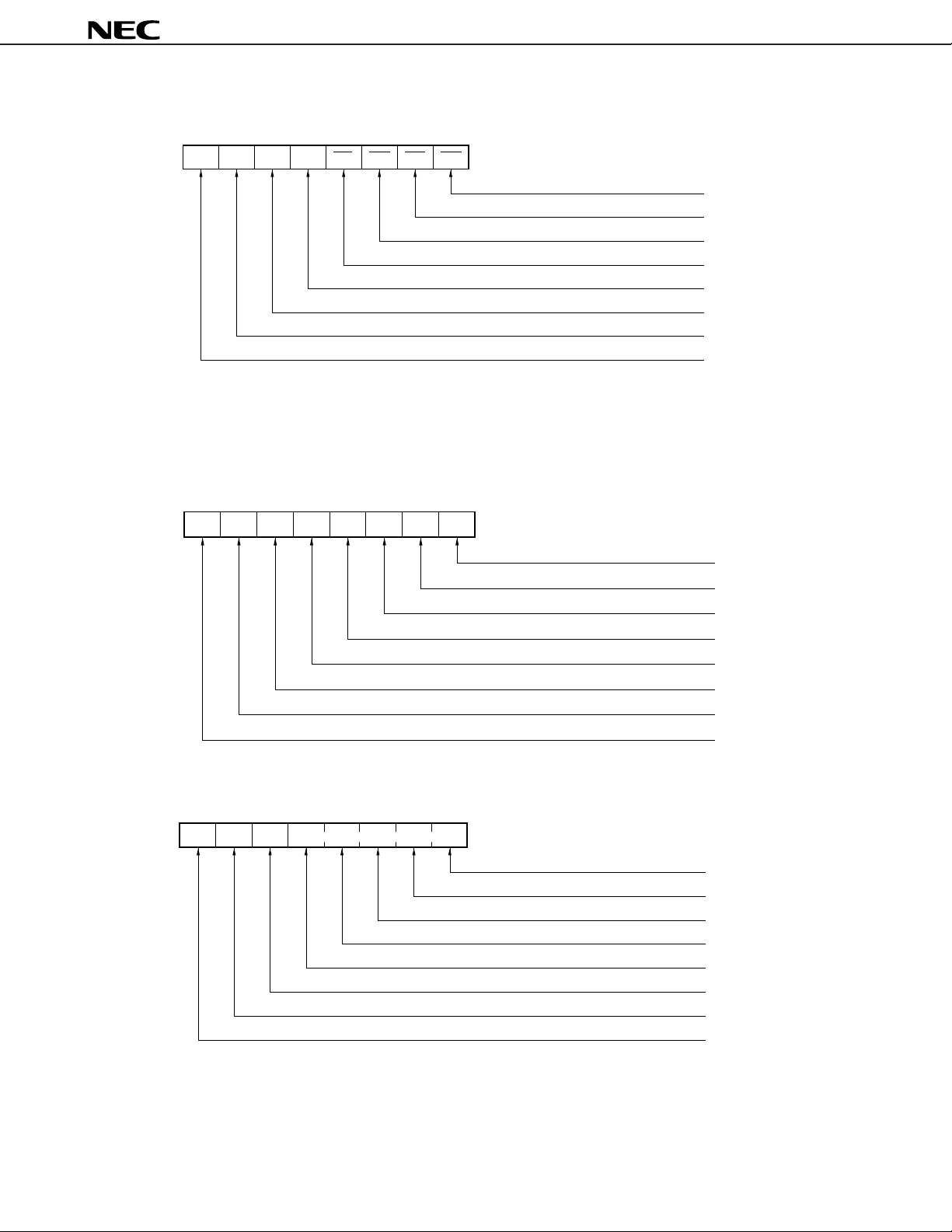
• A/µ-law, power down control
D71D60D5–D4
µ
A/ D3PD1D2PD2D1PD3D0PD4
0/1 Power down/power up for channel 4
0/1 Power down/power up for channel 3
0/1 Power down/power up for channel 2
0/1 Power down/power up for channel 1
0/1 Setting of A-law/ -law
– Don’t care
0 Identification code
1 Identification code
Notes 1. Default setting is power down mode.
2. Default setting is A-law mode.
• Transmit/receive gain setting control (1st word)
µ
PD9611
Note 1
Note 1
Note 1
Note 1
Note 2
µ
D70D61D5–D4–D3
ch1D2ch2D1ch3D0ch4
Transmit/receive gain setting control (2nd word)
D71D61D5
D4 D3 D1 D0
X/R
Setting data
D2
0/1 Gain non-setting/setting for channel 4
0/1 Gain non-setting/setting for channel 3
0/1 Gain non-setting/setting for channel 2
0/1 Gain non-setting/setting for channel 1
– Don’t care
– Don’t care
1 Identification code
0 Identification code
0/1 Gain setting
0/1 Gain setting
0/1 Gain setting
0/1 Gain setting
0/1 Gain setting
0/1 Transmit/receive setting
1 Identification code
1 Identification code
10
Page 11
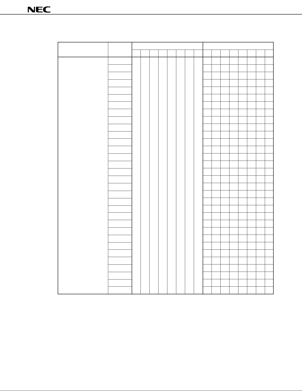
µ
PD9611
Table of Gain Setting Codes
(1/2)
Setting Item Setting 1st Word 2nd Word
Level D7 D6 D5 D4 D3 D2 D1 D0 D7 D6 D5 D4 D3 D2 D1 D0
Gain setting for transmit +7.5 dB 01––ch1ch2ch3ch411010000
+7.0 dB 11010001
+6.5 dB 11010010
+6.0 dB 11010011
+5.5 dB 11010100
+5.0 dB 11010101
+4.5 dB 11010110
+4.0 dB 11010111
+3.5 dB 11011000
+3.0 dB 11011001
+2.5 dB 11011010
+2.0 dB 11011011
+1.5 dB 11011100
+1.0 dB 11011101
+0.5 dB 11011110
Note
0.0 dB
–0.5 dB 11000000
–1.0 dB 11000001
–1.5 dB 11000010
–2.0 dB 11000011
–2.5 dB 11000100
–3.0 dB 11000101
–3.5 dB 11000110
–4.0 dB 11000111
–4.5 dB 11001000
–5.0 dB 11001001
–5.5 dB 11001010
–6.0 dB 11001011
–6.5 dB 11001100
–7.0 dB 11001101
–7.5 dB 11001110
–8.0 dB 11001111
11011111
Note Default setting
11
Page 12
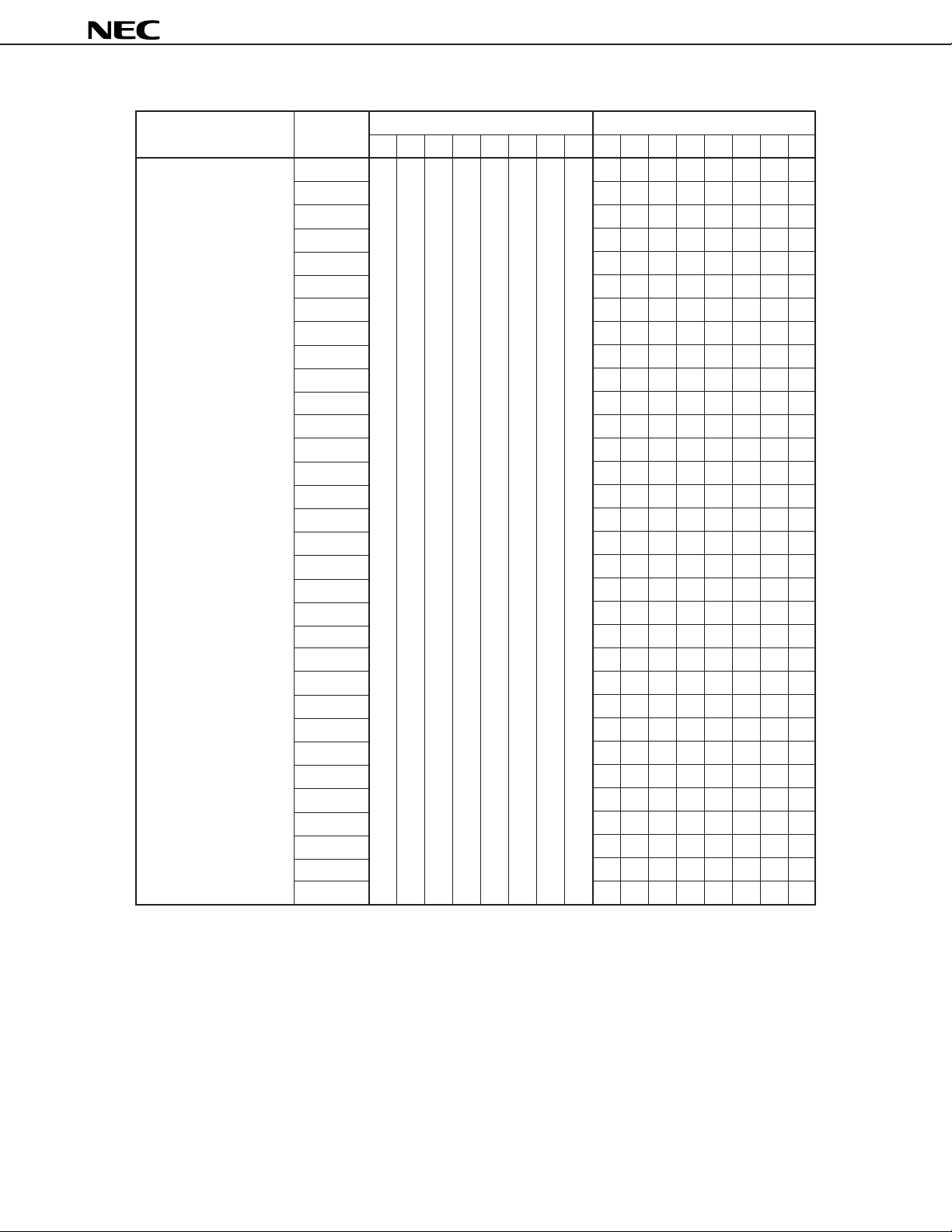
Setting Item Setting 1st Word 2nd Word
Level D7 D6 D5 D4 D3 D2 D1 D0 D7 D6 D5 D4 D3 D2 D1 D0
Gain setting for receive 0.0 dB
Note
01––ch1ch2ch3ch411111111
–0.5 dB 11111110
–1.0 dB 11111101
–1.5 dB 11111100
–2.0 dB 11111011
–2.5 dB 11111010
–3.0 dB 11111001
–3.5 dB 11111000
–4.0 dB 11110111
–4.5 dB 11110110
–5.0 dB 11110101
–5.5 dB 11110100
–6.0 dB 11110011
–6.5 dB 11110010
–7.0 dB 11110001
–7.5 dB 11110000
–8.0 dB 11101111
–8.5 dB 11101110
–9.0 dB 11101101
–9.5 dB 11101100
–10.0 dB 11101011
–10.5 dB 11101010
–11.0 dB 11101001
–11.5 dB 11101000
–12.0 dB 11100111
–12.5 dB 11100110
–13.0 dB 11100101
–13.5 dB 11100100
–14.0 dB 11100011
–14.5 dB 11100010
–15.0 dB 11100001
–15.5 dB 11100000
µ
PD9611
(2/2)
Note Default setting
12
Page 13
µ
PD9611
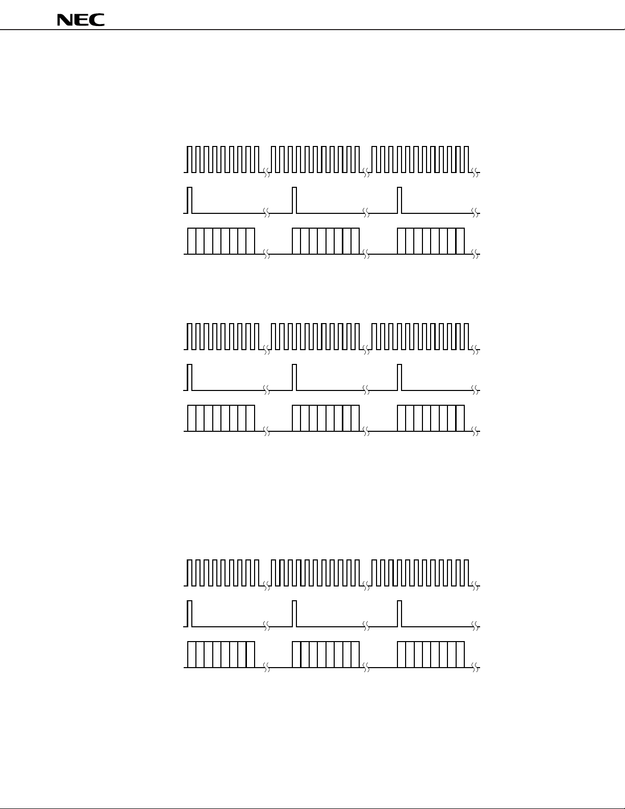
Gain setting control is set by inputting 8-bit data fo the 1st word first and inputting 8-bit data of the 2nd
word in synchronization with the next rising edge of SPSYNC. However, if data other than the identification
code of the 2nd word is input after the input of the 1st word, the contents of the 1st word are ignored.
(i) When gain setting control is valid
SP
CLK
SP
SYNC
SP
DATA
µ
A/ -law, power down control
(valid)
0 1 0 0 1 1 1 1 1101111110001111
Gain setting control (1st word)
(valid)
Gain setting control (2nd word)
(valid)
(ii) When gain setting control is invalid –1
SP
CLK
SP
SYNC
SP
DATA
Gain setting control (1st word)
(invalid)
1 0 0 0 1 1 1 1 1101111101001111
µ
A/ -law, power down control
(valid)
Gain setting control (2nd word)
(invalid)
Remark Because A/µ-law, power down control is input after input of gain setting control (1st word),
gain setting control (1st word) becomes invalid and gain setting control (2nd word) also
becomes invalid.
(iii) When gain setting control is invalid –2
SPCLK
SPSYNC
SPDATA 0 1 0 0 1 1 1 1 1000111111011111
Gain setting control (2nd word)
(invalid)
Gain setting control (1st word)
(invalid)
µ
A/ -law, power down control
(valid)
Remark Because gain setting control (2nd word) is input before gain setting control (1st word), gain
setting control (1st word) becomes invalid. Then, because A/µ-law, power down control
is input even if gain setting control (1st word) is input, gain setting control (1st word)
becomes invalid.
13
Page 14
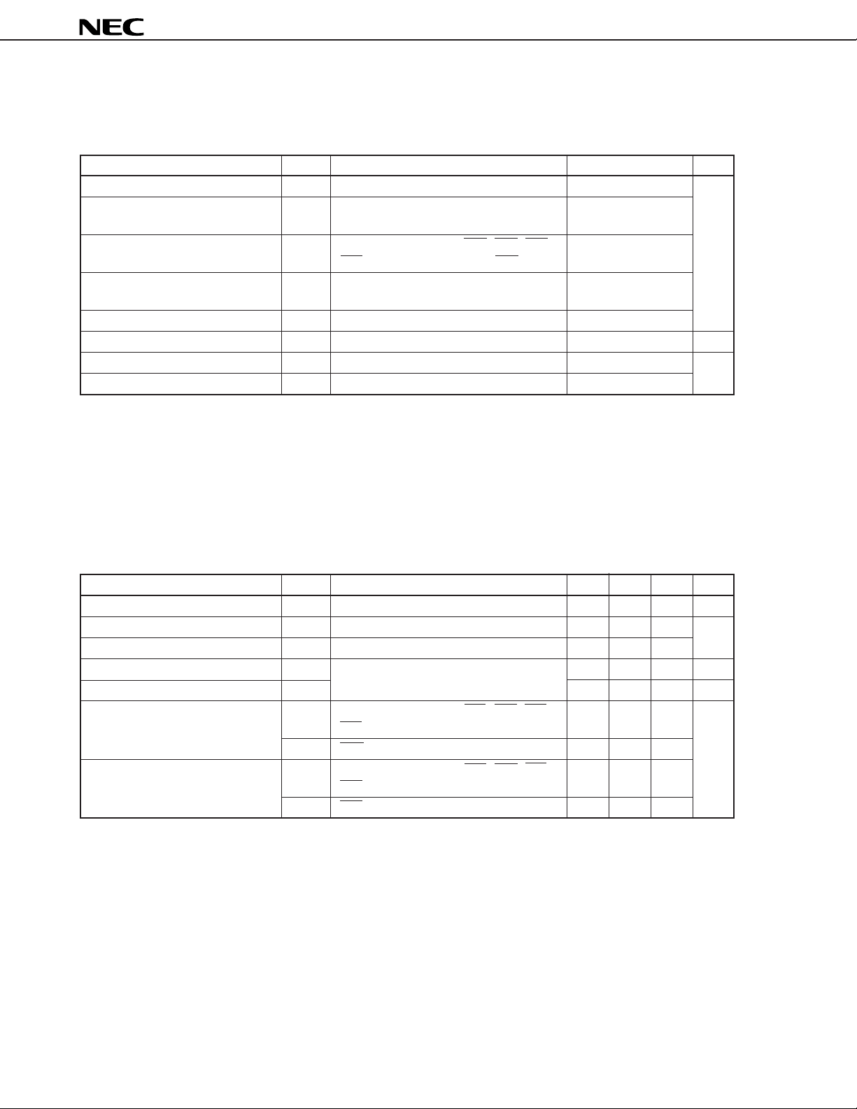
µ
PD9611
4. ELECTRICAL SPECIFICATIONS (PRELIMINARY)
ABSOLUTE MAXIMUM RATINGS (TA = 25 °C)
Item Symbol Condition Rating Unit
Supply voltage VDD AVDD1, AVDD2, AVDD3, AVDD4, DVDD –0.3 to +7.0 V
Analog input voltage VAIN AIN1, AIN2, AIN3, AIN4, ACOMIN1, –0.3 to VDD +0.3
ACOMIN2, ACOMIN3, ACOMIN4
Digital input voltage VDIN DR, DCLR, FSC, LAW, PD1, PD2, PD3, –0.3 to VDD +0.3
PD4, SPCLK, SPSYNC, SPDATA, RST
Voltage applied to analog output VAOUT AOUT1, AOUT2, AOUT3, AOUT4, ACOMOUT1, –0.3 to VDD +0.3
pin ACOMOUT2, ACOMOUT3, ACOMOUT4
Voltage applied to digital output pin VDOUT DX –0.3 to VDD +0.3
Power dissipation PT 500 mW
Ambient operating temperature TA –20 to +85 °C
Storage temperature Tstg –65 to +150
Caution Product quality may suffer if the absolute maximum rating is exceeded for even a single
parameter or even momentarily. That is, the absolute maximum ratings are rated values at
which the product is on the verge of suffering physical damage, and therefore the product must
be used under conditions which ensure that the absolute maximum ratings are not exceeded.
RECOMMENDED OPERATION CONDITIONS (T
A = –20 to +85 °C, VDD = 5 V ± 5 %, GND = 0 V, f DCLK = 2048 kHz)
(1) DC condition
Item Symbol Condition MIN. TYP. MAX. Unit
Ambient operating temperature TA –20 +25 +85 °C
Supply voltage VDD AVDD1, AVDD2, AVDD3, AVDD4, DVDD 4.75 5.0 5.25 V
Analog input voltage VAI
Analog output load resistance RLOAD AOUT1, AOUT2, AOUT3, AOUT450 kΩ
Analog output load capacitance CLOAD 50 pF
High level input voltage VIH1 DR, DCLK, FSC, LAW, PD1, PD2, PD3, 2.0 VDD V
VIH2 RST
Low level input voltage VIL1 DR, DCLK, FSC, LAW, PD1, PD2, PD3, 0 0.8
VIL2 RST 0
AIN1, AIN2, AIN3, AIN4 (ACOM as reference)
PD4, SPCLK, SPSYNC, SPDATA
PD4, SPCLK, SPSYNC, SPDATA
–1.0 +1.0
0.8×VDD
0.2×VDD
VDD
14
Page 15
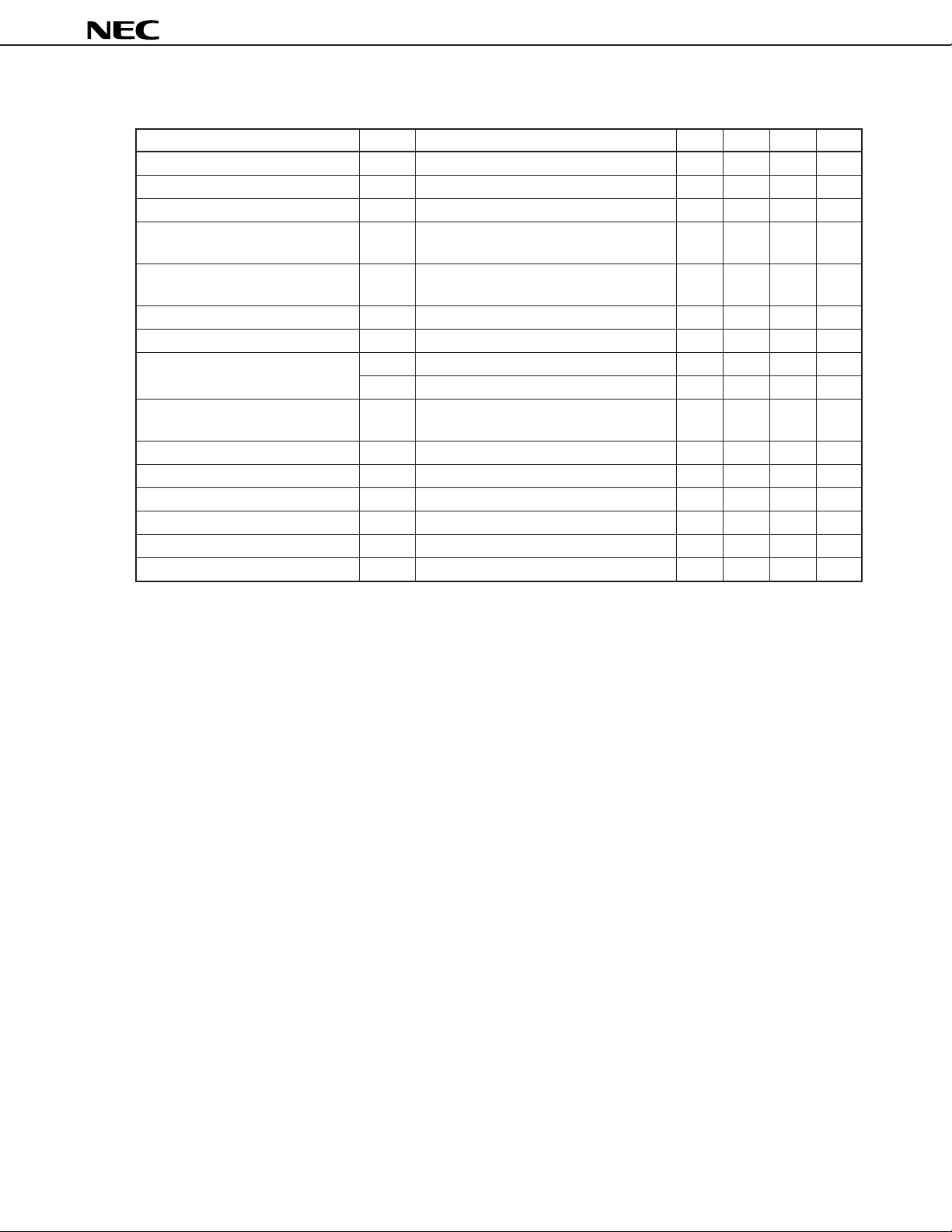
µ
PD9611
(2) AC condition
Item Symbol Condition MIN. TYP. MAX. Unit
Data clock frequency fCLK (= 1/tCY) ±50 ppm 2048 kHz
Data clock pulse width tCLK 200 ns
Frame synchronous clock frequency
High level frame synchronous tWHS 200 ns
pulse width
Low level frame synchronous tWLS 8
pulse width
Clock rise time tR 50 ns
Clock fall time tF 50 ns
Float in synchronous timing tCSD1 100 ns
Frame synchronous clock and tWHSC 100 ns
data clock high level width
DR setup time tDSR Note 65 ns
DR hold time tDHR Note 120 ns
SPDATA clock frequency fSPCLK 2048 kHz
SPDATA setup time tGSR Note 100 ns
SPDATA hold time tGHR Note 100 ns
Float in SP synchronous timing tFSD 40 ns
fs ± 50 ppm 8.0 kHz
µ
tCSD2 40 ns
s
Note Set the rise time and fall time of the digital input waveform and clock signal used for measuring timings
to 5 ns.
15
Page 16
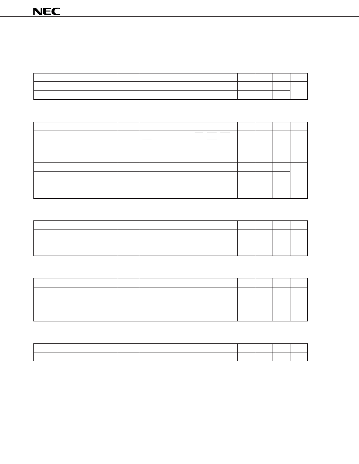
µ
DC CHARACTERISTICS
(TA = –20 to +85 °C, VDD = 5 ± 0.25 V, GND = 0 V, fDCLK = 2048 kHz, and all output pins are unloaded.)
(1) Power consumption
Item Symbol Condition MIN. TYP. MAX. Unit
Circuit current IDD All channels in normal operation 23 30 mA
Power-down circuit current IDDPD All channels in power-down mode 5 6
(2) Digital interface
Item Symbol Condition MIN. TYP. MAX. Unit
Digital input current IID DR, DCLK, FSC, LAW, PD1, PD2, PD3, –10 +10
PD4, SPCLK, SPSYNC, SPDATA, RST
Each pin 0 ≤ VDIN ≤ VDD
3-state leakage current IL DX pin 0 ≤ VDIN ≤ VDD –10 +10
High level output voltage VOH DX pin IOH = –150 µA
Low level output voltage VOL DX pin IOL = 0.8 mA 0.4
Digital output pin output capacitance
Digital input pin input capacitance CID
COD
f = 1 MHz, 0 V other than unmeasured pins
f = 1 MHz, 0 V other than unmeasured pins
VDD–0.3
15 pF
10
PD9611
µ
A
V
(3) Transmit amplifier (AIN1, AIN2, AIN3, AIN4 pins)
Item Symbol Condition MIN. TYP. MAX. Unit
Input bias current IB –10 +10
Input resistance RIN 1MΩ
Input capacitance CIN 10 pF
µ
A
(4) Receive power amplifier (AOUT1, AOUT2, AOUT3, AOUT4 pins)
Item Symbol Condition MIN. TYP. MAX. Unit
Output offset voltage VOA DR = +0 code –50 +50 mV
ACOM as reference
Maximum output voltage VOM ACOM as reference –1.02 +1.02 V
Output resistance ROUT 1 Ω
(5) Signal reference voltage output (ACOMOUT1, ACOMOUT2, ACOMOUT3, ACOMOUT4 pins)
Item Symbol Condition MIN. TYP. MAX. Unit
Output voltage VACOM 2.35 2.4 2.45 V
16
Page 17

µ
PD9611
AC CHARACTERISTICS (TA = –20 to +85 °C, VDD = 5 ± 0.25 V, GND = 0 V, fDCLK = 2048 kHz)
Item Symbol Condition MIN. TYP. MAX. Unit
Data enable delay time tDZX1 DX when FSC is behind DCLK 100 ns
tDZX2 DX when FSC is ahead of DCLK 100 ns
Data delay time tDDX DX pin 100 ns
Data hold time tHZX DX pin 25 ns
17
Page 18
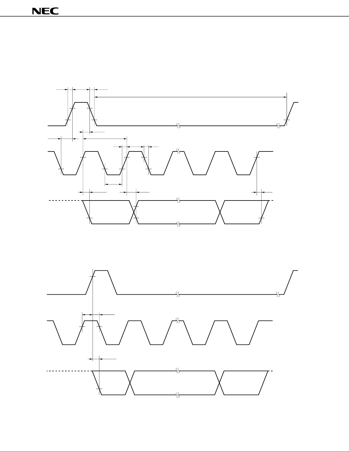
TIMING CHARTS
(1) Transmit timing
(a) When FSC is ahead of DCLK
t
R
t
WHS
FSC
t
t
CSD2
WHSC
µ
PD9611
t
F
t
WLS
t
CY
t
R
t
CLK
t
F
DCLK
Hi-Z Hi-Z
X
(b) When FSC is behind DCLK
FSC
tCSD1
12 8
t
CLK
t
DZX2
MSBD
t
DDX
LSB7th2nd
tWHSC
t
HZX
DCLK
18
12 8
tDZX1
Hi-Z Hi-Z
MSBDX LSB7th2nd
Page 19
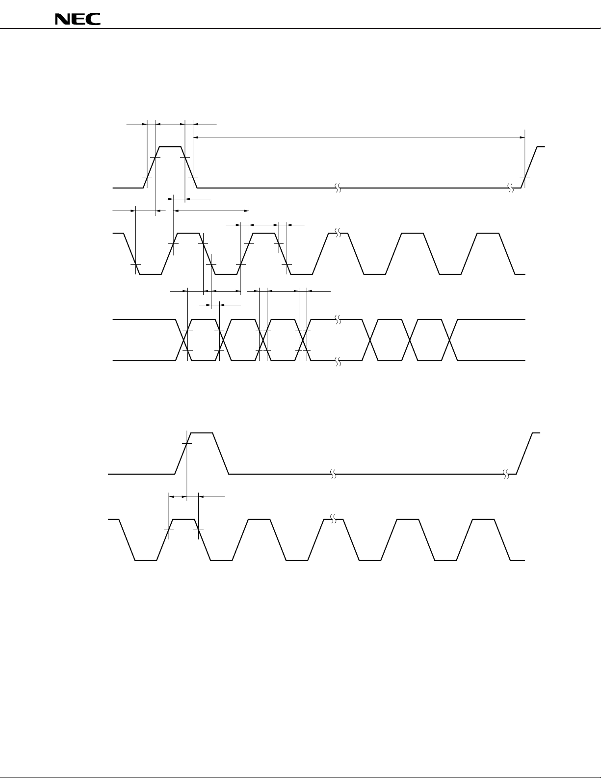
(2) Receive timing
(a) When FSC is ahead of DCLK
t
R
t
FSC
t
CSD2
WHS
t
WHSC
t
F
t
µ
PD9611
t
WLS
CY
t
R
t
CLK
t
F
DCLK
t
DSR
R
Don’t
care
(b) When FSC is behind DCLK
FSC
t
CSD1tWHSC
12 8
tR, t
F
tR, t
t
CLK
t
DHR
MSBD
Don’t
care
F
7th2nd
Don’t
care
8th
9
DCLK
19
Page 20
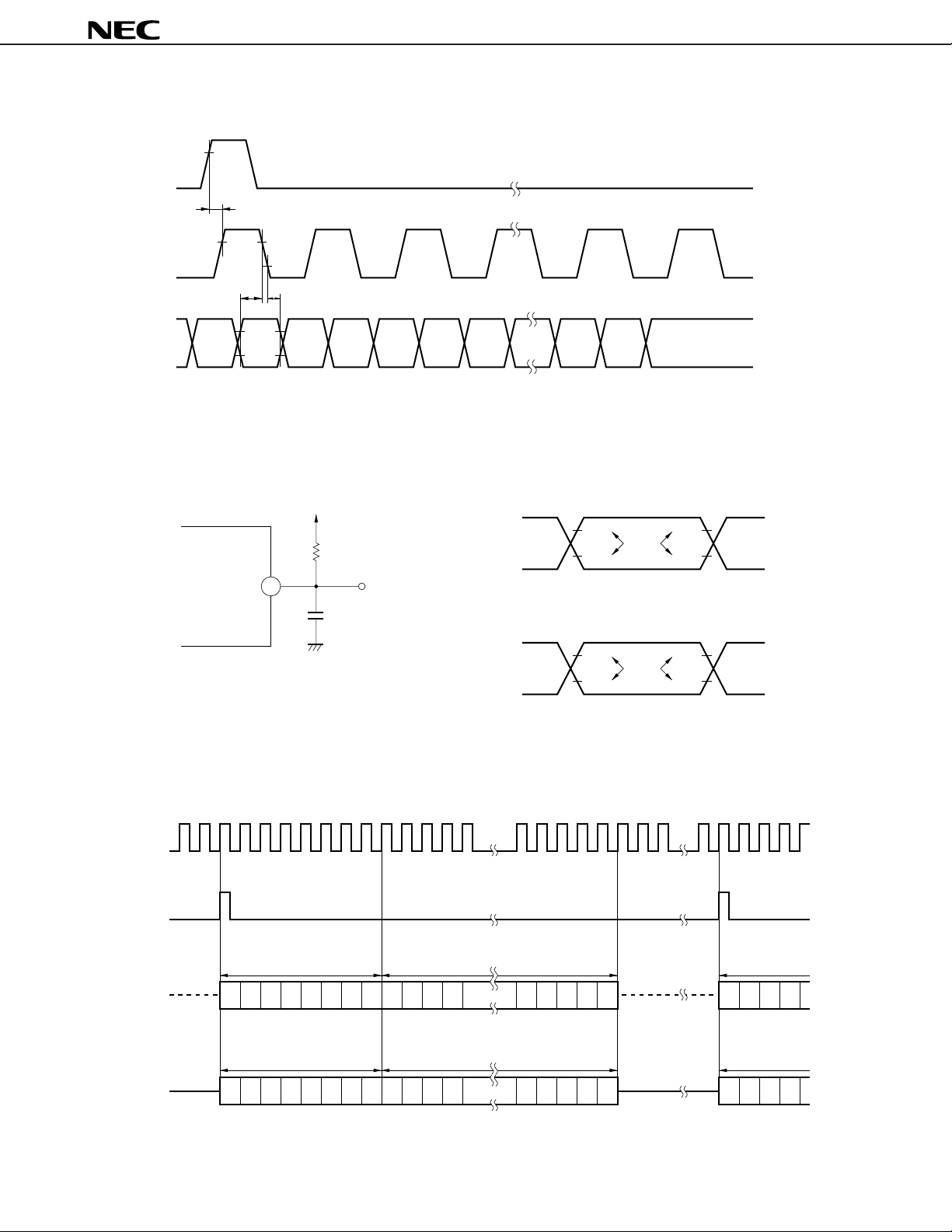
(3) Gain setting timing
SP
SYNC
t
FSD
SP
CLK
123 89
t
GSR
t
GHR
µ
PD9611
SP
DATA
Don’t
care
Remark The relationship between SP
Don’t
D7 D6 D5 D1
care
Don’t
care
SYNC and SPCLK is the same as in the receive timing.
Don’t
care
DX output measuring circuit Timing test waveform
V
DD
2 kΩ
X
D
Output
165 pF
(4) Transmit, receive PCM data input/output timing charts
Don’t
care
D0 Don’t care
All inputs/outputs other than DX pin
2.0 V
0.8 V
Test
points
2.0 V
0.8 V
DX pin output
2.4 V
0.4 V
Test
points
2.4 V
0.4 V
(2.048 MHz)
(8.0 kHz)
20
DCLK
FSC
D
DR
12345678910111213 282930313233 2561234
Channel 1 data
Hi-Z Hi-Z
X
D7 D6 D5 D4 D3 D2 D1 D0 D7 D6 D5 D4 D4 D3 D2 D1 D0 D7 D6 D5 D4
MSB
Channel 1 data
Don’t care
D7 D6 D5 D4 D3 D2 D1 D0 D7 D6 D5 D4 D4 D3 D2 D1 D0 D7 D6 D5 D4
MSB
Channel 2 data
MSB
LSB
Channel 2 data
MSB
LSB
Channel 4 data
LSB
Channel 4 data
LSB
Channel 1 data
SB
Channel 1 data
Don’t care
MSB
Page 21
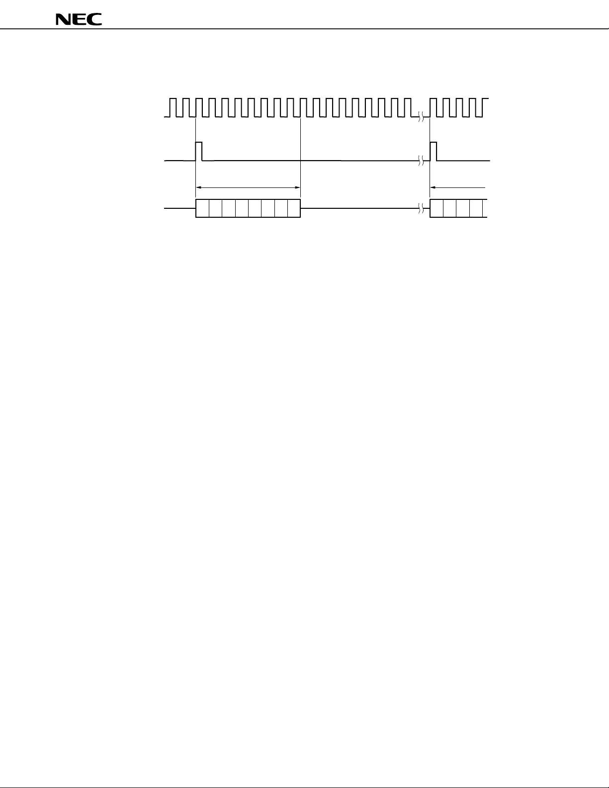
(5) Setting data input timing
1234567891011121314151617 1234
SP
CLK
SP
SYNC
µ
PD9611
SP
Don’t care
DATA
Setting data
D7 D6 D5 D4 D3 D2 D1 D0
MSB LSB
Setting data
Don’t care
D7 D6 D5 D4
MSB
21
Page 22
µ
PD9611
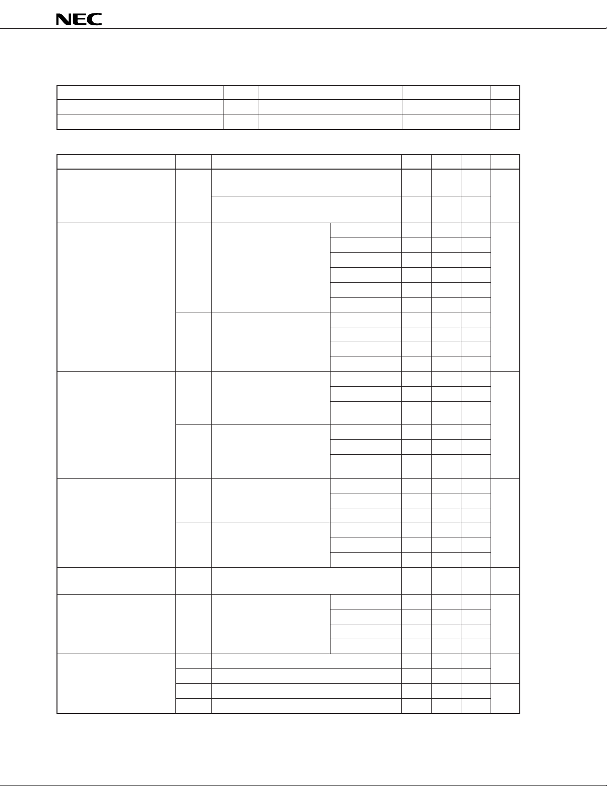
TRANSMISSION CHARACTERISTICS (TA = –20 to +85 °C, VDD = 5 ± 0.25 V, GND = 0 V, fDCLK = 2048 kHz)
Item Symbol Condition Setting Value Unit
Zero transmission level point (transmit) OTLPX Referenced to 600 Ω –3.8 dBm
Zero transmission level point (receive) OTLPX Referenced to 600 Ω –3.8 dBm
Item Symbol Condition MIN. TYP. MAX. Unit
Insertion loss IL A/D input signal –0.3 +0.3 dB
0 dBm0 1 kHz
D/A input signal –0.3 +0.3
0 dBm0 1 kHz
Transmission loss frequency FRX A/D 60 Hz 24.0 – dB
characteristics Reference input signal
1015 Hz 0 dBm0
FRR D/A 0 to 3000 Hz –0.15 +0.15
Reference input signal
1015 Hz 0 dBm0
Gain tracking (tone method) GTX A/D +3 to –40 dBm0 –0.2 +0.2 dB
Reference input signal
–10 dBm0
f = 700 to 1100 Hz
GTR D/A +3 to –40 dBm0 –0.2 +0.2
Reference input signal
–10 dBm0
f = 700 to 1100 Hz
Transmit/receive channel SDX A/D +3 to –30 dBm0 36 dB
overall power distortion ratio
(tone method)
SDR D/A +3 to –30 dBm0 36
Absolute delay characteristic D A A/A 540
Absolute delay distortion DO A/A 500 Hz 1400
frequency characteristics
Idle channel noise ICNADA A/D A-law Psophometric weighted –72 dBm0p
ICNDAA D/A A-law Psophometric weighted –80
ICNADµA/D µ-law C-message weighted 18 dBrnc0
ICNDAµD/A µ-law C-message weighted 10
Input signal –40 dBm0 30
f = 700 to 1100 Hz –45 dBm0 25
Input signal –40 dBm0 30
f = 700 to 1100 Hz –45 dBm0 25
Input signal = 0 dBm0
300 to 3000 Hz –0.15 +0.15
1000 to 2600 Hz 200
200 Hz 0 2.0
3200 Hz –0.15 +0.65
3400 Hz 0 0.8
3780 Hz +6.5
3200 Hz –0.15 +0.65
3400 Hz 0 +0.8
3780 Hz +6.5
–50 dBm0 –0.5 +0.5
–55 dBm0 –1.0 +1.0
–50 dBm0 –0.5 +0.5
–55 dBm0 –1.0 +1.0
600 Hz 700
2800 Hz 1400
µ
s
µ
s
22
Page 23
µ
PD9611
Item Symbol Condition MIN. TYP. MAX. Unit
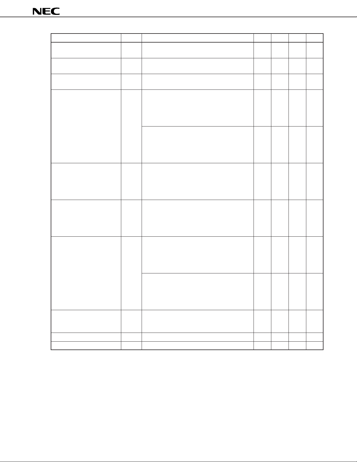
Cross talk between channels CT A/A –70 dB
Input signal = 0 dBm0
Power supply rejection ratio PSRR AVDD1, AVDD2, AVDD3, AVDD4, –25 dB
DVDD = 5 V ± 100 mVP-P
Coder offset A/D –5 +5 –
Input signal 0 V
Mutual modulation (2 tones) IMD A/D 44.0 dB
Input signal:
f1, f2; 300 to 3400 Hz, –4 to –21 dBm0
Measuring signal: 2 × f1 – f2
level (2 × f1 – f2) vs level (f1, f2)
D/A 44.0 dB
Input signal:
f1, f2; 300 to 3400Hz, –4 to –21 dBm0
Measuring signal: 2 × f1 – f2
level (2 × f1 – f2) vs level (f1, f2)
Discrimination A/D –27 dB
Input signal:
f; 4396 to 7796 Hz
0 dBm0
Measuring signal: 8000 – fHz
Out-of-band spurious D/A –27 dB
Input signal:
f; 204 to 3604 Hz
0 dBm0
Measuring signal: 8000 – fHz
In-band spurious A/D –45 dB
Input signal:
f; 700 to 1100 Hz
0 dBm0
Measuring signal: Any frequency
D/A –45 dB
Input signal:
f; 700 to 1100 Hz
0 dBm0
Measuring signal: Any frequency
Single frequency noise NSF D/A –54 dBm0
Gain setting = 0 dB
Measuring signal: f = up to 256 kHz
Transmit gain setting ∆DGSX A/D difference from reference setting value –0.15 +0.15 dB
Receive gain setting ∆DGSR D/A difference from reference setting value –0.15 +0.15
23
Page 24
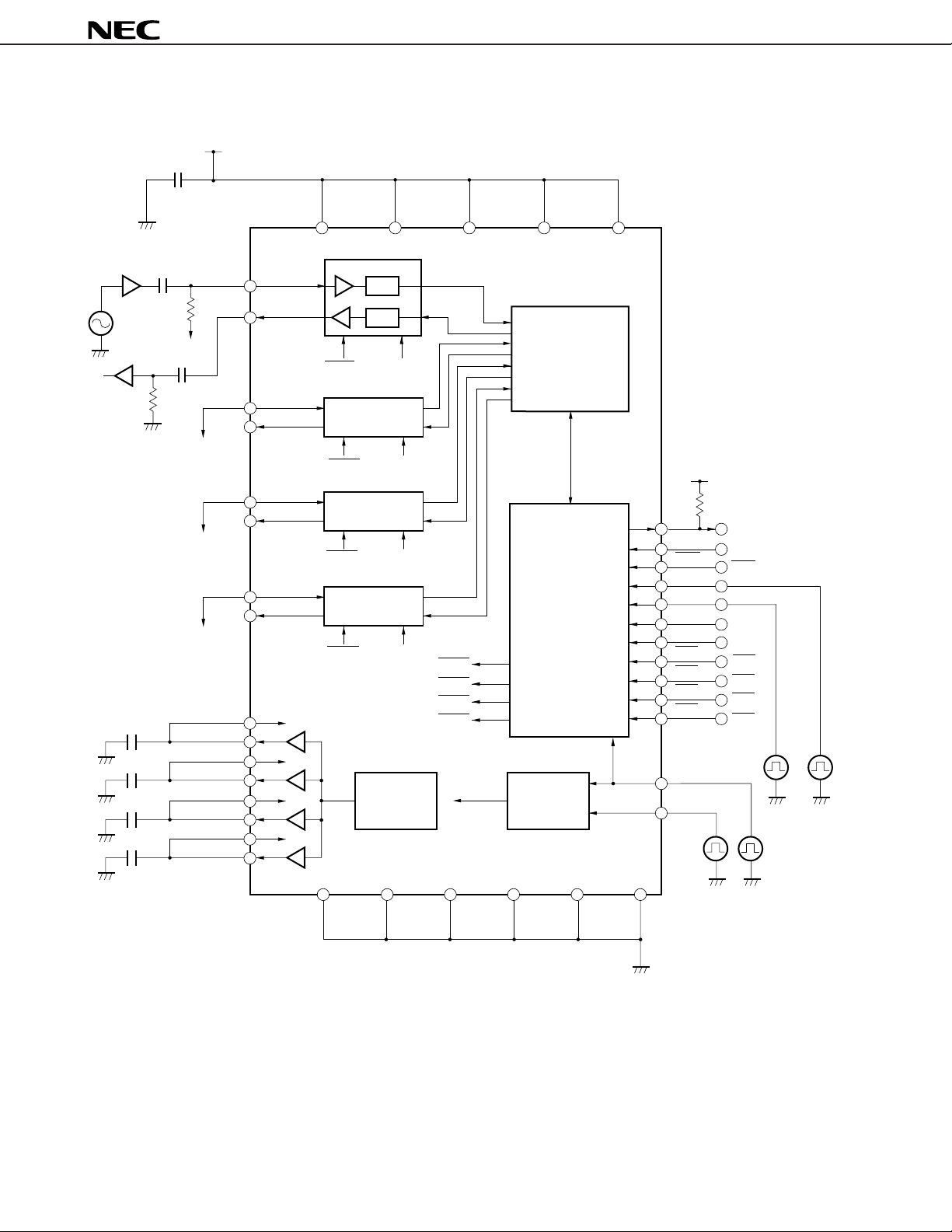
5. APPLICATION CIRCUIT EXAMPLE
VDD
0.1 F
µ
µ
PD9611
100 kΩ
0.1 F
0.1 F
0.1 F
0.1 F
100 kΩ
µ
µ
µ
µ
ACOM
µ
0.1 F
ACOMOUT1
ACOMOUT1
ACOM
ACOMIN1
ACOM
ACOM
ACOM
ACOM
ACOM
ACOM
ACOM
IN
A
1
A
A
A
OUT1
AIN1
OUT
A
IN
OUT
A
IN
OUT
A
IN
OUT
OUT
IN
OUT
IN
OUT
IN
OUT
AVDD1AVDD2AVDD3AVDD4DV
DD
CH1
A/D
1
D/A
DSP
IN
1
APD1
2
ACOM
CH2
Channel FiIter
2
ACOM
IN
APD2
3
3
4
4
1
2
2
3
3
Voltage
Reference
4
2
CH3
ACOMIN3APD3
CH4
I/O
Linear ↔ A,
µ
DGS
ACOMIN4APD4
APD1
MUX, DEMUX
APD2
APD3
APD4
VDD
D
X
D
R
RST
SP
SP
SP
LAW
PD1
PD2
PD3
PD4
SYNC
CLK
DATA
2 kΩ
D
X
D
R
RST
SP
LAW
PD1
PD2
PD3
PD4
SP
DATA
CLK
SP
SYNC
FSC
Clock
Generator
DCLK
FSCDCLK
4
24
0.1 F
µ
AGND1
AGND2 AGND3 AGND4 DGND SUBGND
Page 25
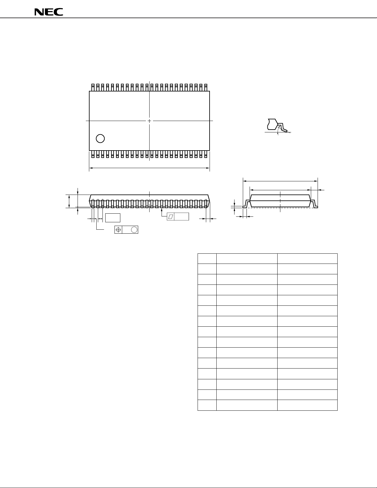
6. PACKAGE DRAWINGS
48 PIN PLASTIC SHRINK SOP (375 mil)
48 25
detail of lead end
–3°
+7°
3°
µ
PD9611
124
A
G
F
E
C
M
M
D
N
NOTE
Each lead centerline is located within 0.10
mm (0.004 inch) of its true position (T.P.) at
maximum material condition.
H
I
K
B
L
P48GT-65-375B-1
ITEM MILLIMETERS INCHES
0.639 MAX.
0.025 MAX.
0.026 (T.P.)
+0.004
0.012
–0.005
0.005±0.003
0.079 MAX.
0.067±0.004
+0.012
0.394
–0.013
0.315±0.008
+0.009
0.039
–0.008
+0.004
0.006
–0.002
+0.008
0.020
–0.009
0.004
0.004
M
A
B
C
D
E
F
G
H
I
J
K
L
16.21 MAX.
0.63 MAX.
0.65 (T.P.)
0.30±0.10
0.125±0.075
2.0 MAX.
1.7±0.1
10.0±0.3
8.0±0.2
1.0±0.2
+0.10
0.15
–0.05
0.5±0.2
0.10
N
0.10
J
25
Page 26
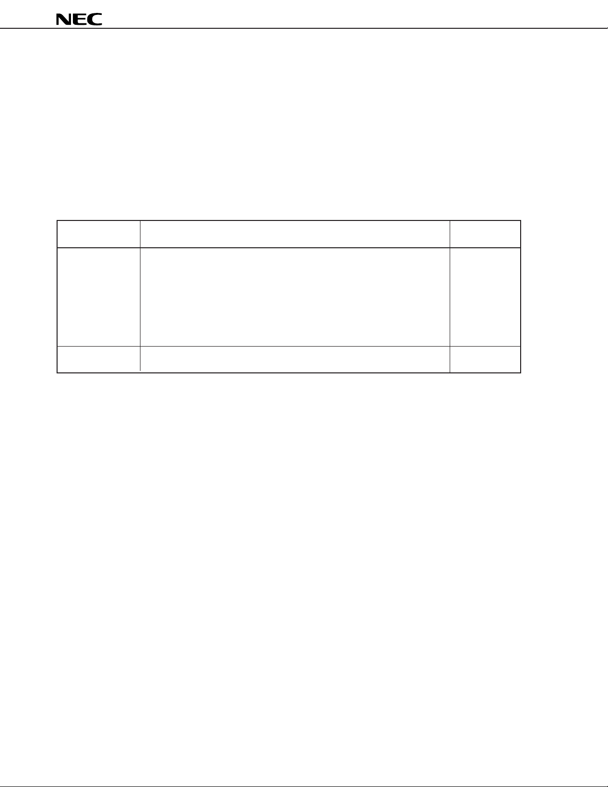
7. RECOMMENDED SOLDERING CONDITIONS
This product should be soldered and mounted under the conditions recommended below.
For details of recommended soldering conditions, refer to the information document Semiconductor Device
Mounting Technology Manual (C10535E).
For soldering methods and conditions other than those recommended, please contact your NEC sales
representative.
SURFACE MOUNT TYPE
µ
PD9611GT: 48-pin shrink SOP (375 mil)
µ
PD9611
Soldering Method Soldering Conditions
Infrared reflow Package peak temperature: 235 °C IR-35-103-2
Duration: 30 sec. max. (210 °C or above)
Number of times: 2 max.
Time limit: 3 days
<Cautions>
(1) Wait for the device temperature to return to normal after the first reflow
before starting the second reflow.
(2) Do not perform flux cleaning with water after the first reflow.
Pin heating Pin temperature: 300 °C max. —
Duration: 3 sec. max. (per side of device)
Note
(thereafter, 10-hour prebaking at 125 °C required.)
Recommended
Condition Symbol
Note For the storage period after unpacking from the dry-pack, storage conditions are max. 25 °C, 65 % RH.
26
Page 27
NOTES FOR CMOS DEVICES
1 PRECAUTION AGAINST ESD FOR SEMICONDUCTORS
Note: Strong electric field, when exposed to a MOS device, can cause destruction
of the gate oxide and ultimately degrade the device operation. Steps must
be taken to stop generation of static electricity as much as possible, and
quickly dissipate it once, when it has occurred. Environmental control must
be adequate. When it is dry, humidifier should be used. It is recommended
to avoid using insulators that easily build static electricity. Semiconductor
devices must be stored and transported in an anti-static container, static
shielding bag or conductive material. All test and measurement tools
including work bench and floor should be grounded. The operator should
be grounded using wrist strap. Semiconductor devices must not be touched
with bare hands. Similar precautions need to be taken for PW boards with
semiconductor devices on it.
µ
PD9611
2 HANDLING OF UNUSED INPUT PINS FOR CMOS
Note: No connection for CMOS device inputs can be cause of malfunction. If no
connection is provided to the input pins, it is possible that an internal input
level may be generated due to noise, etc., hence causing malfunction. CMOS
device behave differently than Bipolar or NMOS devices. Input levels of
CMOS devices must be fixed high or low by using a pull-up or pull-down
circuitry. Each unused pin should be connected to VDD or GND with a
resistor, if it is considered to have a possibility of being an output pin. All
handling related to the unused pins must be judged device by device and
related specifications governing the devices.
3 STATUS BEFORE INITIALIZATION OF MOS DEVICES
Note: Power-on does not necessarily define initial status of MOS device. Produc-
tion process of MOS does not define the initial operation status of the device.
Immediately after the power source is turned ON, the devices with reset
function have not yet been initialized. Hence, power-on does not guarantee
out-pin levels, I/O settings or contents of registers. Device is not initialized
until the reset signal is received. Reset operation must be executed immediately after power-on for devices having reset function.
27
Page 28

µ
PD9611
[MEMO]
The application circuits and their parameters are for reference only and are not intended for use in actual design-ins.
No part of this document may be copied or reproduced in any form or by any means without the prior written
consent of NEC Corporation. NEC Corporation assumes no responsibility for any errors which may appear in
this document.
NEC Corporation does not assume any liability for infringement of patents, copyrights or other intellectual property
rights of third parties by or arising from use of a device described herein or any other liability arising from use
of such device. No license, either express, implied or otherwise, is granted under any patents, copyrights or other
intellectual property rights of NEC Corporation or others.
While NEC Corporation has been making continuous effort to enhance the reliability of its semiconductor devices,
the possibility of defects cannot be eliminated entirely. To minimize risks of damage or injury to persons or
property arising from a defect in an NEC semiconductor device, customers must incorporate sufficient safety
measures in its design, such as redundancy, fire-containment, and anti-failure features.
NEC devices are classified into the following three quality grades:
"Standard", "Special", and "Specific". The Specific quality grade applies only to devices developed based on a
customer designated "quality assurance program" for a specific application. The recommended applications of
a device depend on its quality grade, as indicated below. Customers must check the quality grade of each device
before using it in a particular application.
Standard: Computers, office equipment, communications equipment, test and measurement equipment,
audio and visual equipment, home electronic appliances, machine tools, personal electronic
equipment and industrial robots
Special: Transportation equipment (automobiles, trains, ships, etc.), traffic control systems, anti-disaster
systems, anti-crime systems, safety equipment and medical equipment (not specifically designed
for life support)
Specific: Aircrafts, aerospace equipment, submersible repeaters, nuclear reactor control systems, life
support systems or medical equipment for life support, etc.
The quality grade of NEC devices is "Standard" unless otherwise specified in NEC's Data Sheets or Data Books.
If customers intend to use NEC devices for applications other than those specified for Standard quality grade,
they should contact an NEC sales representative in advance.
Anti-radioactive design is not implemented in this product.
M4 96.5
 Loading...