

Page 1
DATA SHEET
GaAs INTEGRATED CIRCUIT
µ
PG110P
2 to 8 GHz WIDE BAND AMPLIFIER CHIP
DESCRIPTION
The µPG110P is a GaAs monolithic integrated circuit designed as a wide band amplifier from 2 to 8 GHz. And
the device is available in chip form. The µPG110P is suitable for the gain stage required high gain characteristic of
the microwave communication system and the measurement equipment.
FEATURES
• Ultra wide band : 2 to 8 GHz
• High Power Gain : GP = 15 dB TYP. @f = 2 to 8 GHz
• Medium Power : P
O(1 dB) = +14 dBm TYP. @f = 2 to 8 GHz
ORDERING INFORMATION
PART NUMBER FORM
µ
PG110P Chip
ABSOLUTE MAXIMUM RATINGS (TA = 25 °C)
Supply Voltage VDD +10 V
Input Voltage V
Input Power Pin +10 dBm
Total Power Dissipation Ptot*
Operating Temperature T
Storage Temperature Tstg –65 to +125 °C
*1 Mounted with AuSn hard solder
*2 The temperature of base material beside the chip
RECOMMENDED OPERATING CONDITIONS (TA = 25 °C)
Supply Voltage VDD +8 ± 0.2 V
Input Power P
in –5 dBm
IN –5 to +0.6 V
opr*
1
2
1.5 W
–65 to +125 °C
Document No. P11882EJ2V0DS00 (2nd edition)
(Previous No. ID-2454)
Date Published September 1996 P
Printed in Japan
©
1989
Page 2
µ
PG110P
ELECTRICAL CHARACTERISTICS (TA = 25 °C)
CHARACTERISTIC SYMBOL MIN. TYP. MAX. UNIT TEST CONDITIONS
Supply Current IDD 65 135 180 mA VDD = +8 V
Power Gain GP 12 15 dB
Gain Flatness
Input Return Loss RLin 610 dB
Output Return Loss RLout 710 dB
Isolation ISL 30 40 dB
Output Power at 1 dB PO(1 dB) 10 14 dBm
Gain Compression Point
*3
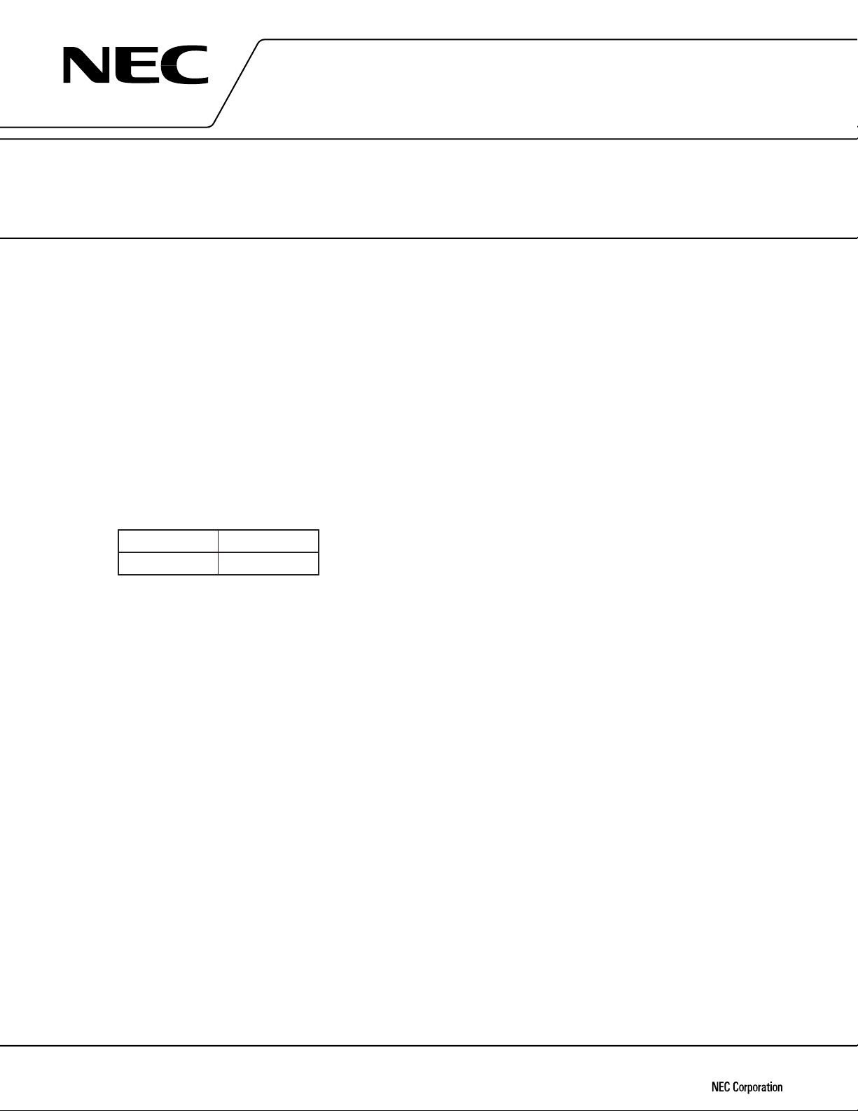
These characteristics are based on performance of devices mounted in the standard package shown in Fig. 1
∆
GP ±1.5 dB
*3
f = 2 to 8 GHz
Fig. 1 4 pin Ceramic Package
Top View
4.5 MAX.
0.6
± 0.06
.
+0.2
–0.1
0.7
4.1 MIN.
0.1 ± 0.06
4.6 MAX.
0.4 ± 0.06
4.1 MIN.
1.48 MAX.
2
Page 3
µ
PG110P
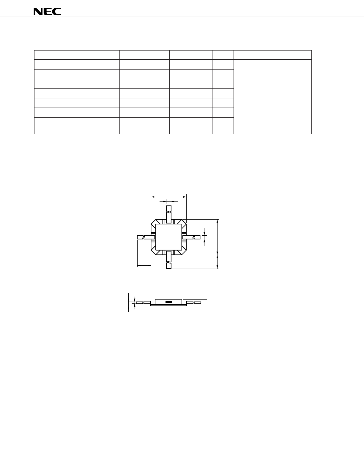
TYPICAL CHARACTERISTICS (TA = 25 °C)
POWER GAIN vs. FREQUENCY
30
20
10
- Power Gain - dB
P
G
0
012345678910
INPUT RETURN LOSS vs. FREQUENCY
0
*4
VDD = +8 V
IDD = 132 mA
f - Frequency - GHz
VDD = +8 V
IDD = 132 mA
RL
–10
in
–20
RL
out
- Output Return Loss - dB
- Input Return Loss - dB
in
out
–30
RL
RL
012345678910
f - Frequency - GHz
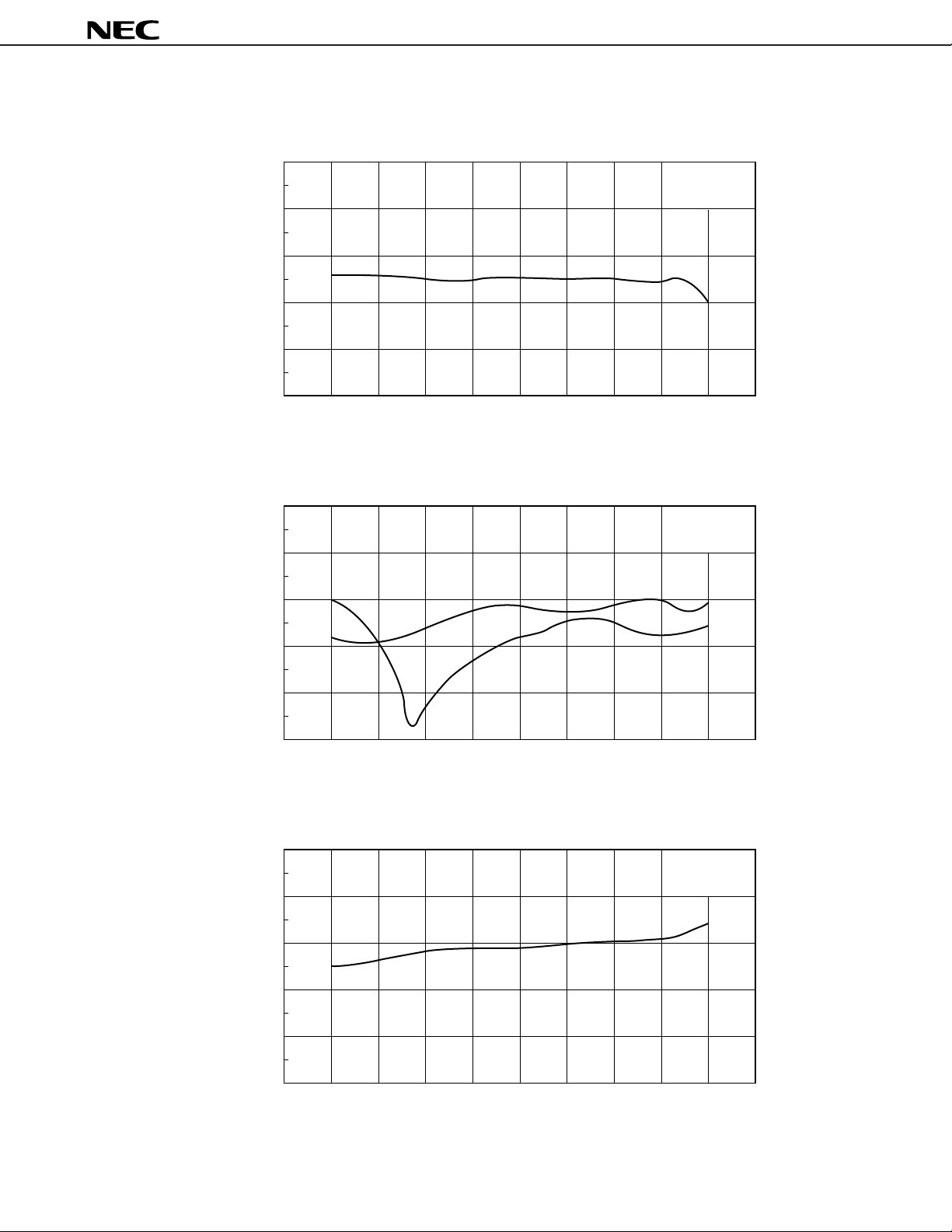
ISOLATION vs. FREQUENCY
0
DD
= +8 V
V
IDD = 132 mA
–20
–40
–60
ISL - Isolation - dB
–80
012345678910
f - Frequency - GHz
3
Page 4

OUTPUT POWER vs. INPUT POWER
20
10
- Output Power - dBm
out
P
0
DD
= +8 V
V
I
DD
= 132 mA
f = 2 GHz
f = 5 GHz
f = 8 GHz
µ
PG110P
–20 –10 0 10
Pin - Input Power - dBm
*4 These characteristics are measured for device mounted in the standard package shown in Fig. 1.
EQUIVALENT CIRCUIT
V
DD
Active
R
R
R
L1
L
L1
R
F1
in
IN
L
L
1
R
G1
R
L
G1
S1
C
1
R
G2
C
S
L2
L
L2
L
2
C
R
C
4
F2
2
G3
Load
L
L3
L
3
3
C
OUT
C
RF
4
Page 5

RECOMMENDED CHIP ASSEMBLY CONDITIONS
µ
Die Attachment
Atmosphere : N2 gas
Temperature : 320 ± 5 °C
t
AuSn Preform: 0.5 × 0.5 × 0.05
* The hard solder such as AuSi or AuGe which has higher melting point than AuSn should not
be used.
Base Material : CuW, Cu, KV
* Other material should not be used.
Epoxy Die Attach is not recommended.
Bonding
Machine : TCB
* USB is not recommended
µ
Wire : 30
m diameter Au wire
Temperature : 260 ± 5 °C
Strength : 31 ± 3 g
Atmosphere : N
2 gas
(mm), 1 pce.
µ
PG110P
Chip Bonding Diagram
V
DD
50 to
µ
100 m
V
500 to
µ
1 000 m
IN
200 to 500 m
DD
less than 300 m
µ
5
GND
OUT
200 to
µ
500 m
µ
GND
1
2
GND
GND
not used less than 200 m
3
GND
4
5
Page 6

Recommended Wire Length
1. 500 to 1 000 µm for Input (the longer the wire, the better the VSWR)
µ
2. 200 to 500
3. It should be bonded via a chip capacitor for VDD.
Wire length is 200 to 500 µm
4. There are five GND pads but GND pad <2> is not used.
Wire length is 200
Less than 300 µm for <5>.
Chip Size: 1.1 × 1.3 mm
Pad Size : 100 × 100 µm
m for Output (the shorter the wire, the better the VSWR)
µ
m for <1>, <3> and <4>.
µ
t = 140
m
µ
PG110P
6
Page 7

µ
PG110P
QUALITY ASSURANCE (Refer to GET-30116)
1. 100 % Tests
1-1 100 % DC Probe
1-2 Visual Inspection
MIL-STD-883 Method 2010 Condition B
2. Tests on Sampling Basis
2-1 Bond Pull Tests (In case of recommended chip handling)
MIL-STD-883 Method 2011
5 samples/wafer and 20 points tested
Accept 0/Reject 1
2-2 Tests in Standard Package
µ
Test the electrical characteristics of chips assembled into the standard package used for
5 samples/wafer tested
DC and RF measurement Accept 1/Reject 2
3. Warrantee
NEC has a responsibility of quality assurance for the products within 180 days after delivered to customers where these
are handled properly and stored in a desiccater with the flow of dry N
2 gas.
PG110B
4. Caution
4-1 Take great care to prevent static electricity.
4-2 Be sure that Die Attach is performed in N
2 atmosphere.
7
Page 8

µ
PG110P
Caution
The Great Care must be taken in dealing with the devices in this guide.
The reason is that the material of the devices is GaAs (Galium Arsenide), which is
designated as harmful substance according to the law concerned.
Keep the law concerned and so on, especially in case of removal.
No part of this document may be copied or reproduced in any form or by any means without the prior written
consent of NEC Corporation. NEC Corporation assumes no responsibility for any errors which may appear in
this document.
NEC Corporation does not assume any liability for infringement of patents, copyrights or other intellectual property
rights of third parties by or arising from use of a device described herein or any other liability arising from use
of such device. No license, either express, implied or otherwise, is granted under any patents, copyrights or other
intellectual property rights of NEC Corporation or others.
While NEC Corporation has been making continuous effort to enhance the reliability of its semiconductor devices,
the possibility of defects cannot be eliminated entirely. To minimize risks of damage or injury to persons or
property arising from a defect in an NEC semiconductor device, customers must incorporate sufficient safety
measures in its design, such as redundancy, fire-containment, and anti-failure features.
NEC devices are classified into the following three quality grades:
"Standard", "Special", and "Specific". The Specific quality grade applies only to devices developed based on a
customer designated "quality assurance program" for a specific application. The recommended applications of
a device depend on its quality grade, as indicated below. Customers must check the quality grade of each device
before using it in a particular application.
Standard: Computers, office equipment, communications equipment, test and measurement equipment,
audio and visual equipment, home electronic appliances, machine tools, personal electronic
equipment and industrial robots
Special: Transportation equipment (automobiles, trains, ships, etc.), traffic control systems, anti-disaster
systems, anti-crime systems, safety equipment and medical equipment (not specifically designed
for life support)
Specific: Aircrafts, aerospace equipment, submersible repeaters, nuclear reactor control systems, life
support systems or medical equipment for life support, etc.
The quality grade of NEC devices is "Standard" unless otherwise specified in NEC's Data Sheets or Data Books.
If customers intend to use NEC devices for applications other than those specified for Standard quality grade,
they should contact an NEC sales representative in advance.
Anti-radioactive design is not implemented in this product.
M4 96.5
 Loading...