

Page 1
# 580 Pleasant Street
Watertown, MA 02472
Phone:(617) 926-0404
F A X : (617) 924-1235
Features
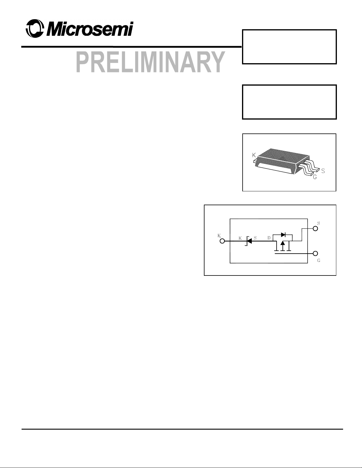
POWERMITE 3 Surface Mount Package
•
MOSFET with Schottky Rectifier for reverse voltage blocking
•
Single 3 leaded device replaces 2 individual components
•
Integral Heat Sink / Locking Tabs
•
Supplied in 16mm Tape and Reel – 6000 units/reel
•
Superior Low Thermal and Electrical capability
•
UPFS320P
SURFACE MOUNT
P – CHANNEL
MOSKEY
Mechanical Characteristics
Footprint Area of 16.51 mm
•
Case: Molded Epoxy
•
Meets UL94VO at 1/8 inch
•
Weight: 72 milligrams
•
Lead and Mounting Temperatures: 260
•
2
C max for 10 seconds
°°°°
Description
The MOSK EY
fier to provide reverse blocking capability in a single three
leaded package. This device is well suited for applications
such as battery chargers and switching where the intrinsic
source-drain diode is an undesirable feature.
Note: Vks = Vds (Mosfet) + Vf (Rectifier)
Absolute Maximum Ratings at 25°C
RATING SYMBOL VALUE
Cathode-to-Source Voltage VKSS +/- 20
Gate-to-Source Voltage VGS +/- 8 Vdc
Cathode Current:
Continuous @ TA=25
Single Pulsed IKM 11.0
Total Power Dissipation PD (1)
Storage Temperature T stg
Operating Temperature
combines a MOSFET with a Schottky Recti-
C
°°°°
IK 3.0 Adc
2.0 Watts
-55 to 150
T op -55 to 150
UNIT
Apk
C C
°°°°
C C
°°°°
Vdc
Thermal Characteristics
Thermal Resistance:
Junction to Tab Rjtab 5
(1)Junction-to-tab Rja (1) 60
(2)Junction-to-ambient Rja (2) 120
(1) Mounted on 2” square by 0.06’ thick FR4 board with a 1” x1” square 2 ounce copper pattern.
(2) Mounted on 0.06 thick FR4 board, using recommended footprint, with 2 ounce copper
MSC 02-17-00
PRELIMINARY
C/Watt
°°°°
C/Watt
°°°°
C/Watt
°°°°
Page 2
UPFS320P
Electrical Characteristics at 25°C
ELECTRICAL CHARACTERISTICS (TA = 25 C unless otherwise noted)
Symbol Parameter Conditions Min Typ Max Units
OFF CHARACTERISTICS
BVKSS Cathode-Source Breakdown Voltage VGS= 0V; IK = 250uA 20 V
IKSSF Zero Gate Voltage Cathode Current:
Forward
IKSSR Zero Gate Voltage Cathode
Current:Reverse
IGSS Gate-Body Leakage Current VGS= +/- 8V, VDS = 0V 100 nA
ON CHARACTERISTICS (pulsed 500us max, duty cycle < 2%)
VGS(TH) Gate Threshold Voltage VDS > VGS; IK = 250uA 0.4 0.6 1 V
DELTA
VGS(TH)/
Gate Threshold Voltage Temp
Coefficient
TJ
VKS (ON) Static Cathode-Source On Voltage VGS = 4.5 V; IK = 3A 700 mV
VKS (ON) Static Cathode-Source On Voltage VGS = 4.5 ; IK = 1A 400 mV
IK(ON) On State Cathode Current VGS = 4.5 V; VKS = 5V 10 A
Gfs Forward Transconductance VDS = 10 V; IK = 3 A 6.5 S
DYNAMIC CHARACTERISTICS
Ciss Input Capacitance VKS = 10 V; VGS = 0V, F = 1 MHz 700 pF
Coss Output Capacitance VKS = 10 V; VGS = 0V, F = 1MHz 270 pF
Crss Reverse Transfer Capacitance VKS = 10 V; VGS = 0V, F = 1MHz 100 pF
SWITCHING CHARACTERISTICS
Td
(ON)
Turn On Delay Time
Tr Turn On Rise Time
Td
(OFF)
Turn Off Delay time
Tf Turn Off Fall time
Qg Total Gate Charge VDS = 5V, IK = 3A, VGS = 4.5V 9.5 13 nC
Qgs Gate-Source Charge VDS = 5V, IK = 3A, VGS = 4.5V 1.3 nC
Qgd Gate-Cathode Charge VDS = 5V, IK = 3A, VGS = 4.5V 2.2 nC
VKS= -16V, VGS = 0V 1 uA
VKS= +16V, VGS = 0V 1.5 mA
IK = 250uA, Reference to 25C 2.1 mV/C
VDD = 5V, IK = 1A, VGS = 4.5V, Rg = 6
VDD = 5V, IK = 1A, VGS = 4.5V, Rg = 6
VDD = 5V, IK = 1A, VGS = 4.5V, Rg = 6
VDD = 5V, IK = 1A, VGS = 4.5V, Rg = 6
ΩΩΩΩ
ΩΩΩΩ
ΩΩΩΩ
ΩΩΩΩ
816 ns
24 38 ns
50 80 ns
29 45 ns
MSC 02-17-00
PRELIMINARY
Page 3

UPFS320P
MSC 02-17-00
PRELIMINARY
Page 4

UPFS320P
MSC 02-17-00
PRELIMINARY
Page 5

UPFS320P
MECHANICAL SPECIFICATIONS
MSC 02-17-00
PRELIMINARY
 Loading...