

Page 1
DATA SHEET
MOS INTEGRATED CIRCUIT
µ
PD9930
LINEAR CODEC FOR DIGITAL CELLULAR TELEPHONE
The µPD9930 is a +3 V single power operation, low power consumption linear CODEC LSI developed for digital
cellular telephone use.
CODEC has a wide dynamic use.
This IC also features a microphone/receiver amplifier, a tone generator, DAI (Digital Audio Interface: conforming
to GSM11.10), and a power-saving function. These functions can be controlled by microcontroller.
In addition, 21 mW (TYP.) low power consumption is enabled during 3 V operation.
FEATURES
• +3 V single power supply
• Low power consumption
In operation: 7 mA (TYP.) (VDD = 3 V)
In stand-by mode: 50 µA (TYP.) (VDD = 3 V)
• CODEC
• 13-bit precision linear coding
• Transmission level can be controlled by microcontroller.
• Analog input/output funciton
• Low noise microphone amplifier
• High output receiver amplifier
Piezo-electric receiver can be directly driven.
Gain canbe controlled by microcontroller.
• On-chip amplifier for accessory input/output
• Tone generator
• Frequency, generating pattern and gain can be controlled
by microcontroller.
• DTMF generation function
• Various service tone generation function
• GSM triple tone generation function
• Desired tone frequency can be registered (0.3 to 3.4 kHz)
ORDERING INFORMATION
Part Number Package
µ
PD9930G-22 44-pin plastic QFP (10 × 10 mm)
• DAI
• Conforming to GSM11.10
• Test mode can be set by terminal or microcontroller
command.
• Stand-by mode
• Rise time at time of stand-by clearing: 30.5 ms (TYP.)
• Master clock generation PLL (external clock input: 8 kHz)
• Tone interrupt pattern output function
• Ringer output function
The information in this document is subject to change without notice.
Document No. S11616EJ2V0DS00 (2nd edition)
(Previous No. IC-3342)
Date Published November 1996 N
Printed in Japan
The mark shows major revised points.
©
1994,1996
Page 2
2
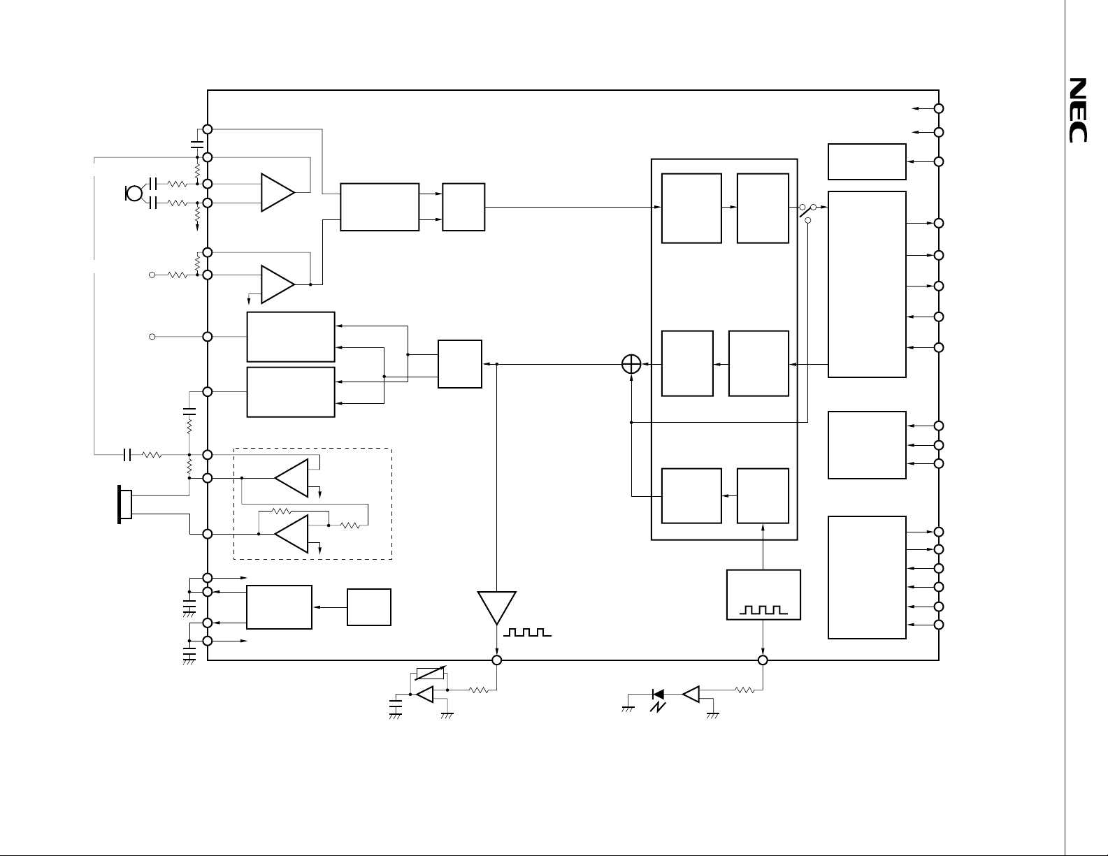
BLOCK DIAGRAM
RESETB
(15 to 33 dB)
(to XACOMO)
(0 to 10 dB)
REC2O–
REC2O+
XACOMI
XACOMO
RACOMO
MIXI
MICO
MICI–
MICI+
XAUXO
XAUXI–
RAUXO
REC1O
REC2I–
Microphone
amplifier
–
+
Accessory input
amplifier
to V
–
+
ref
Post Filter 1
(Accessory output
amplifier)
0 dB fix
Post Filter 2
(Receiver amplifier 1)
0 to -31 dB
(1 dB steps)
Receiver drive amplifier
(Receiver amplifier 2)
V
combuff
Digital signal processor
PLL
Voice send
Pre-Filter
+ Mixer
0 or –3 dB
A/D
Digital
Gain Cont.
0 to –2.8 dB
(0.4 dB steps)
Transmit
BPF
DSP
INTERFACE
Voice receive
D/A
Receive
LPF
Digital
Gain Cont.
0 to –2.4 dB
(0.8 dB steps)
MICRO-
CONTROLLER
INTERFACE
–
+
to V
ref
Sign code
output
Tone
Gain Cont.
0 to –30 dB
(1 dB steps)
–38.5 dB
Tone
Generator
–
+
to V
ref
DAI
Tone Interval
(GSM11. 10)
Generation
V
ref
REQB
FSYNC
(8 kHz)
SCLK
(256 kHz)
SEN
SO
SI
DSPSEL
MCLK
MSTR
MDAT
DCLK
DO
DI
TC1
TC2
DRSTB
RACOMI
RINGER
Low-current drive LED
TIMER
µ
PD9930
Page 3
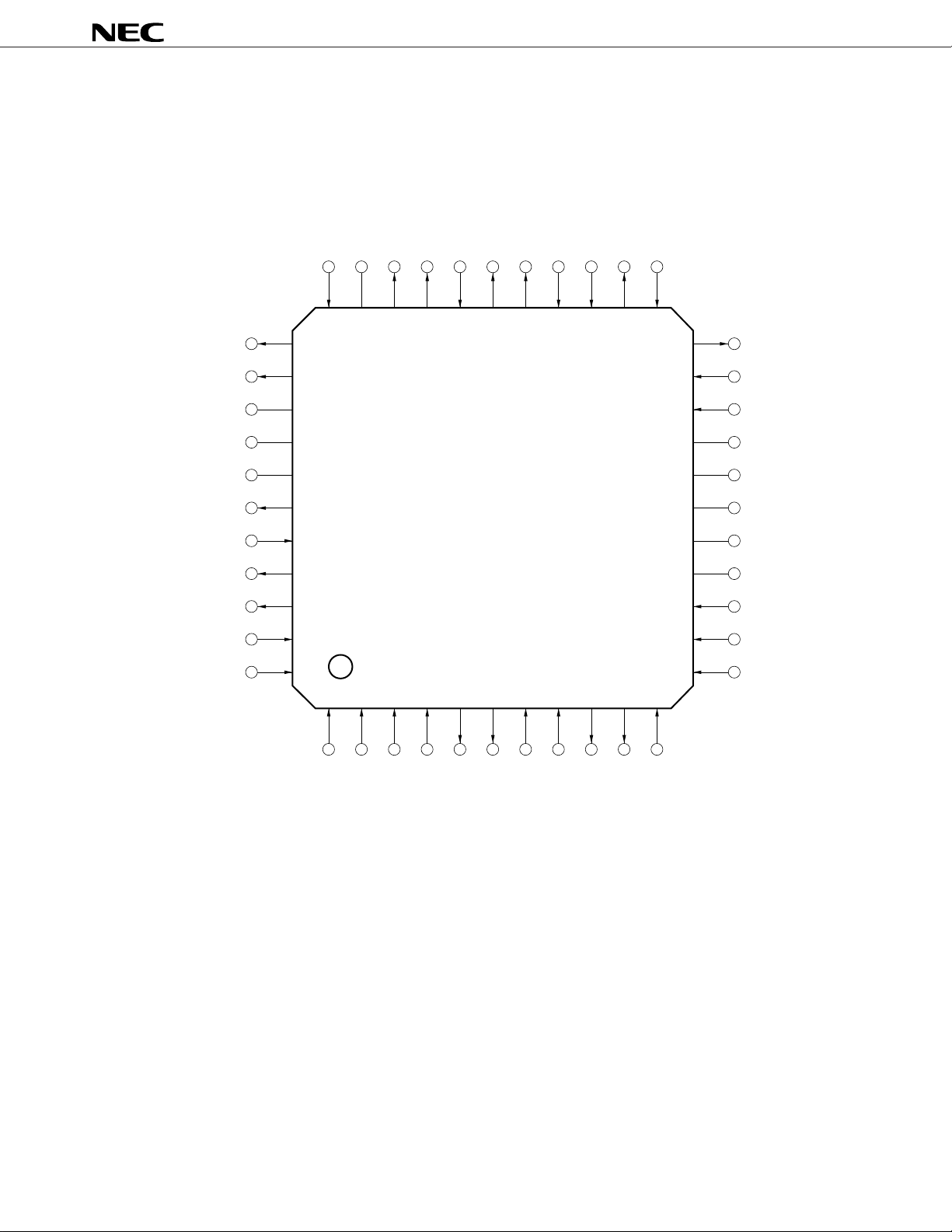
PIN CONFIGURATION (Top View)
44-pin plastic QFP (10 x 10 mm)
Note
REC2I–
IC
33 32 31 30 29 28 27 26 25 24 23
REC1O
34
REC2O–
REC2O+
RACOMI
RACOMO
XACOMO
XACOMI
XAUXI–
XAUXO
MIXI
22
µ
PD9930
MICO
RAUXO
DD1
AV
AV
DD2
DV
SEN
SO
SCLK
TEST
MSTR
35
36
37
DD
SI
38
39
40
41
42
43
44
1234567891011
DI
MDAT
MCLK
DO
DRSTB
DCLK
TC1
TC2
TIMER
RINGER
DSPSEL
21
20
19
18
17
16
15
14
13
12
MICI–
MICI+
AGND4
AGND3
AGND2
AGND1
DGND
FSYNC
RESETB
REQB
Note Internal connection; leave unconnected
3
Page 4

Pin Name
AGND1-AGND4 : Analog Ground
AVDD1, AVDD2 : Analog Power Supply
DCLK : DAI (Digital Audio Interface) Clock Output
DGND : Digital Ground
DI : DAI Serial Input
DO : DAI Serial Output
DRSTB : DAI Reset
DSPSEL : Digital Signal Processor Select
DD : Digital Power Supply
DV
FSYNC : Frame Synchronization Signal Input
IC : Internally Connected
MCLK : Microcontroller Synchronous Clock
MDAT : Microcontroller Serial Data
MICI+ : Microphone Amplifier Input Non-Inverted
MICI– : Microphone Amplifier Input Inverted
MICO : Microphone Amplifier Output
MIXI : Mixer Input
MSTR : Microcontroller Strobe
RACOMI : Receive Common Reference Voltage Input
RACOMO : Receive Common Reference Voltage Output
RAUXO : Receive Auxiliary Amplifier Output
REC1O : Receive Amplifier 1 Output
REC2I– : Receive Amplifier 2 Input Inverted
REC2O+ : Receive Amplifier 2 Output Non-Inverted
REC2O– : Receive Amplifier 2 Output Inverted
REQB : Request
RESETB : Reset
RINGER : Ringer
SCLK : Serial Data Synchronous Clock Output
SEN : Serial Data Output Enable
SI : Serial Data Input
SO : Serial Data Output
TC1, TC2 : DAI Mode Control
TEST : Test
TIMER : Timer
XACOMI : Transmit Common Reference Voltage Input
XACOMO : Transmit Common Reference Voltage Output
XAUXI– : Transmit Auxiliary Amplifier Input Inverted
XAUXO : Transmit Auxiliary Amplifier Output
µ
PD9930
4
Page 5

µ
PD9930
CONTENTS
1. PIN FUNCTIONS ...........................................................................................................................6
1.1 LIST OF PIN FUNCTIONS ..................................................................................................................... 6
1.2 PIN EQUIVALENT CIRCUIT .................................................................................................................. 8
2. BLOCK FUNCTIONS .....................................................................................................................9
2.1 CODEC .................................................................................................................................................... 9
2.1.1 Audio Codec..............................................................................................................................9
2.1.2 Audio Analog Input .................................................................................................................. 9
2.1.3 Audio Analog Output ............................................................................................................. 10
2.1.4 Audio Digital Accessory Output ........................................................................................... 11
2.1.5 Audio Digital Signal Processor ............................................................................................ 11
2.1.6 Power Up/Down Control ........................................................................................................ 12
2.1.7 Microcontroller Interface ....................................................................................................... 18
2.1.8 DSP Interface .......................................................................................................................... 19
2.1.9 DAI (Digital Audio Interface) ................................................................................................. 22
3. TONE INTERVAL OUTPUT FUNCTION (TIMER TERMINAL)................................................. 29
4. INTERNAL CONTROL FUNCTIONS ...........................................................................................30
4.1 SEND/RECEIVE GAIN CONTROL ...................................................................................................... 30
4.1.1 Voice Send Analog Gain/Receiver Amplifier 2 Control Register (TXGCR) .................... 32
4.1.2 Voice Receive Analog Gain Control Register (RXGCR) ................................................... 3 3
4.1.3 Voice Send/Receive Digital Gain Control Register (DGGSR) .......................................... 35
4.2 DIGITAL INPUT/OUTPUT CONTROL ................................................................................................. 37
4.2.1 Digital Signal Processing Control Register (DSPCR) ....................................................... 38
4.3 TONE CONTROL..................................................................................................................................40
4.3.1 Tone Frequency Selection Register (FRQSR)....................................................................43
4.3.2 Expanded Tone Registers (EXPR1, EXPR2) ....................................................................... 45
4.3.3 Tone Control Register (TONCR)...........................................................................................47
4.3.4 Tone Gain Control Register (TNGCR) ................................................................................. 48
4.4 TEST MODE CONTROL ...................................................................................................................... 50
4.4.1 Test Control Register (TSTCR).............................................................................................52
5. ELECTRICAL CHARACTERISTICS ............................................................................................53
6. APPLIED CIRCUIT EXAMPLE ....................................................................................................73
7. PACKAGE DRAWINGS ...............................................................................................................74
8. RECOMMENDED SOLDERING CONDITIONS ......................................................................... 7 5
5
Page 6
1. PIN FUNCTIONS
1.1 LIST OF PIN FUNCTIONS
Table 1-1 List of Pin Functions (1/2)
Pin No. Pin Name Input/Output Function
1 MDAT Input Microcontroller interface serial input
2 MCLK Input Microcontroller interface clock input
3 DRSTB Input DAI (Digital Audio Interface) reset input
This is reset at low level. Internally pulled high.
4 DI Input DAI serial input
Internally pulled high.
5 DO Output DAI serial output
Hi-Z in normal operation (TC1 = TC2 = low level)
6 DCLK Output DAI clock output (104 kHz)
Hi-Z in normal operation
7 TC1 Input
8 TC2 Input
DAI mode control
Selection of test mode specified by
GSM11.10 in combination with TC1
and TC2
L: Low level
H: High level
TC2 TC1 Test mode specification
L L Normal operation
L H Speech encoder test mode
H L Speech decoder test mode
H H Acoustic device test mode
µ
PD9930
TC1 and TC2 pins are internally pulled down.
9 TIMER Output Timer output. Output of rectangular wave synchronized with tone intermittent
pattern.
10 RINGER Output Ringer tone output. Output of rectangular wave synchronized with tone fre-
quency.
11 DSPSEL Input Selection of DSP interface input/output timing mode.
Connect to VDD or GND. (VDD = mode 1, GND = mode 2)
12 REQB Input Input of DSP interface data transmit request signal.
Serial data can be input/output at low level.
13 RESETB Input System reset input. This is reset at low level. Initializes all control registers.
Reset when turning power on.
14 FSYNC Input Send/receive frame synchronization signal (8 kHz) input
15 DGND — Digital ground. Connect to a digital ground line near µPD9930 pins.
16 AGND1 — Analog ground. Connect to an analog ground line near µPD9930 pins.
17 AGND2 —
18 AGND3 —
19 AGND4 —
20 MICI+ Input Microphone amplifier non-inverted input
21 MICI– Input Microphone amplifier inverted input
22 MICO Output Microphone amplifier output. Connect microphone amplifier gain adjust resistor.
Outputs sidetone signal to REC2I- pin.
23 MIXI Input Pre-filter + mixer input
24 XAUXO Output Accessory input amplifier output. Connect accessory input amplifier gain adjust
resistor.
6
Page 7
µ
Table 1-1 List of Pin Functions (2/2)
Pin No. Pin Name Input/Output Function
25 XAUXI– Input Accessory input amplifier inverted input
26 XACOMI Input Voice send internal reference voltage input
27 XACOMO Output Voice send internal reference voltage (1.2 V) output
28 RACOMO Output Voice receive internal reference voltage (1.2 V) output
29 RACOMI Input Voice receive internal reference voltage input
30 REC2O+ Output Receiver amplifier 2 non-inverted output
31 REC2O– Output Receiver amplifier 2 inverted output
32 IC — Internal connection; leave unconnected
33 REC2I– Input Receiver amplifier 2 inverted input
Connect sidetone gain adjust resistor.
34 REC1O Output Receiver amplifier 1 output
35 RAUXO Output Accessory output amplifier output
36 AVDD1 — Analog power. Connect to an analog power supply line near µPD9930 pins.
37 AVDD2 —
38 DVDD — Digital power. Connect to a digital power supply line near µPD9930 pins.
39 SEN Output DSP interface enable signal output
40 SI Input DSP interface serial input
41 SO Output DSP interface serial output
42 SCLK Output DSP interface clock output (256 kHz)
43 TEST Input Set at high level
44 MSTR Input Microcontroller interface strobe signal input
PD9930
Caution Short-circuit the XACOMI and XACOMO pins at a location as close to the pins of the µPD9930 as
possible. Connect a capacitor (chip capacitor or electrolytic capacitor) between this short-circuited
portion and analog ground.
The same applies to the RACOMI and RACOMO pins.
The transmission/reception level is determined by these reference pins. Therefore, make sure that
these pins are not affected by noise or fluctuation of ground potential due to current.
7
Page 8
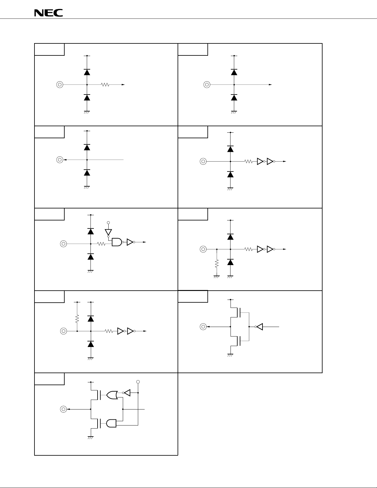
1.2 PIN EQUIVALENT CIRCUIT
AV
DD
µ
PD9930
Type 2Type 1
AV
DD
Analog input
To internal circuit
AGND
Pin Name MICI+, MICI–, XAUXI–, REC2I–
AV
Type 3
DD
Analog output
From internal circuit
AGND
Pin Name MICO, XAUXO, XACOMO, RACOMO,
REC2O+, REC2O–, REC1O, RAUXO
DV
Type 5
DD
Mask input
CMOS input
To internal
circuit
Analog input
AGND
Pin Name MIXI, XACOMI, RACOMI
DV
Type 4
DD
CMOS input
DGND
Pin Name MDAT, MCLK, DSPSEL, REQB,
RESETB, FSYNC, TEST, MSTR
Note
Type 6
DV
DD
CMOS input
To internal circuit
To internal
circuit
To internal
circuit
Pin Name SI
Note
Type 7
DV
DD
CMOS input
Pin Name DRSTB, DI
Type 9
CMOS output
Pin Name DO, DCLK
DV
DD
P
N
DGND
DGND
DD
DV
DGND
To internal
circuit
Enable signal
From internal
circuit
DGND
Pin Name TC1, TC2
Type 8
DV
DD
P
CMOS output
N
DGND
Pin Name TIMER, RINGER, SEN, SO, SCLK
From internal
circuit
Note In normal mode, set the output of drive IC side to high impedance for reducing power consumption.
8
Page 9
2. BLOCK FUNCTIONS
2.1 CODEC
2.1.1 Audio Codec
Audio analog signal and linear code conversion.
• Input/output format: 16 bits (2's complement)
• Accuracy: 13 bits
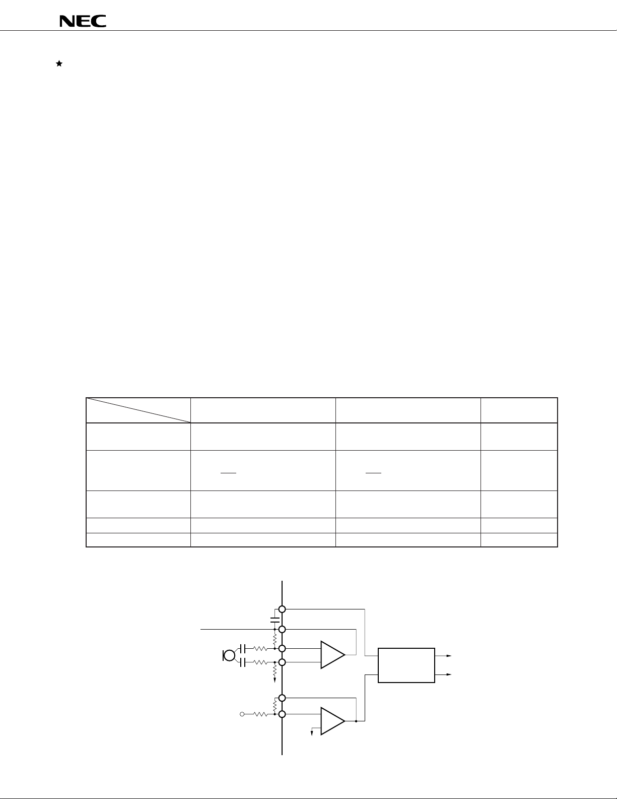
2.1.2 Audio Analog Input
Includes microphone input and accessory input.
(1) Microphone amplifier
Amplifiers differential input signals from the microphone to the required gain.
(2) Accessory input amplifier
Amplifiers the accessory input signal to the required gain.
µ
PD9930
(3) Pre-filter + mixer
Selects the output signal of microphone amplifier and accessory input amplifier, and inputs these to A/D converter
after controlled gain.
Table 2-1 Analog Input Function
Amplifier
Function
Gain setting method External resistor External resistor Microcontroller
Gain setting range 15 to 33 dB 0 to 10 dB 0 or –3 dB
20 log (dB) 20 log (dB)
Minimum resistive load 50 kΩ 300 kΩ —
(Including gain setting resistance) (Including gain setting resistance)
Maximum capacitive load 20 pF 20 pF —
Maximum output level 0.6 V0-p 0.6 V0-p —
Microphone Amplifier Accessory Input Amplifier Pre-filter + Mixer
command
R2 R3
R1 R4
Figure 2-1 Analog Input Block
MIXI
(15 to 33 dB)
(to XACOMO)
(0 to 10 dB)
R1
R1
R4
R2
R3
MICO
MICI–
MICI+
XAUXO
XAUXI–
to V
Microphone
amplifier
–
+
–
+
Accessory input amplifier
ref
Pre-filter +
mixer
0 or –3 dB
9
Page 10
µ
PD9930
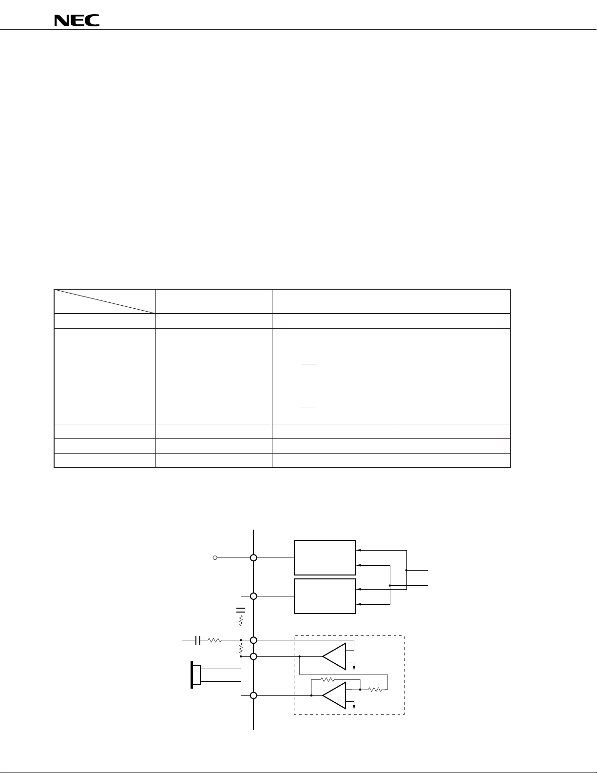
2.1.3 Audio Analog Output
Includes receiver output and accessory output. Sidetone addition is also possible.
(1) Post filter 2 (receiver amplifier 1)
This circuit adjusts the gain of D/A differential output signal (volume control), and then converts it to single output
signal.
(2) Receiver drive amplifier (receiver amplifier 2)
This is differential output amplifier that can directly drive a piezo-electric receiver (when using a dynamic receiver,
an additional external amplifier is necessary). The sidetone is added in this circuit.
(3) Post filter 1 (accessory output amplifier)
This circuit converts D/A differential output signal to single output signal. Connected to the earphone of the head
set (capacitance load), etc.
Table 2-2 Analog Output Functions
Amplifier
Function
Gain setting method Microcontroller command External resistor —
Gain setting range 0 to –31 dB (1 dB steps) Voice receive signal gain: —
Minimum resistive load 100 kΩ 2 kΩ 100 kΩ
Maximum capacitive load 20 pF 60 nF 100 pF
Maximum output level 0.6 V0-p 4 Vp-p (Differential output) 0.6 V0-p
Receiver Amplifier 1 Receiver Amplifier 2 Accessory Output Amplifier
– ∞ to + 10 dB
R3
20 log (dB) + 6 dB
R2
Sidetone signal gain:
– ∞ to + 3 dB
R3
20 log (dB) + 6 dB
R1
Note
Note
Note Conversion result (single output → differential output)
Figure 2-2 Analog Output Block
Post filter 1
(accessory output
amplifier)
0 dB fix
Post filter 2
(receive amplifier 1)
0 to –31 dB
(1 dB steps)
Receiver drive amplifier
(receiver amplifier 2)
–
+
to V
ref
Sidetone signal
R1
R2
R3
RAUXO
REC1O
REC2I–
REC2O–
10
REC2O+
–
+
to V
ref
Page 11
µ
PD9930
2.1.4 Audio Digital Accessory Output
(1) Ringer output (RINGER pin)
• Outputs rectangular waves of the same signal frequency as tone signal frequency.
• The output is controlled by turning off power to the output buffer with a control register.
Figure 2-3 RINGER Output
RAUXO
(Tone output)
RINGER
The RINGER signal tends to bounce when the tone output (RAUXO) signal crosses its zero level, and this
tendency increases as the tone output gain decreases (lower than 0 dB).
When using RINGER pin, tune the tone output gain by TNGCR (Tone gain control register) to 0 dB.
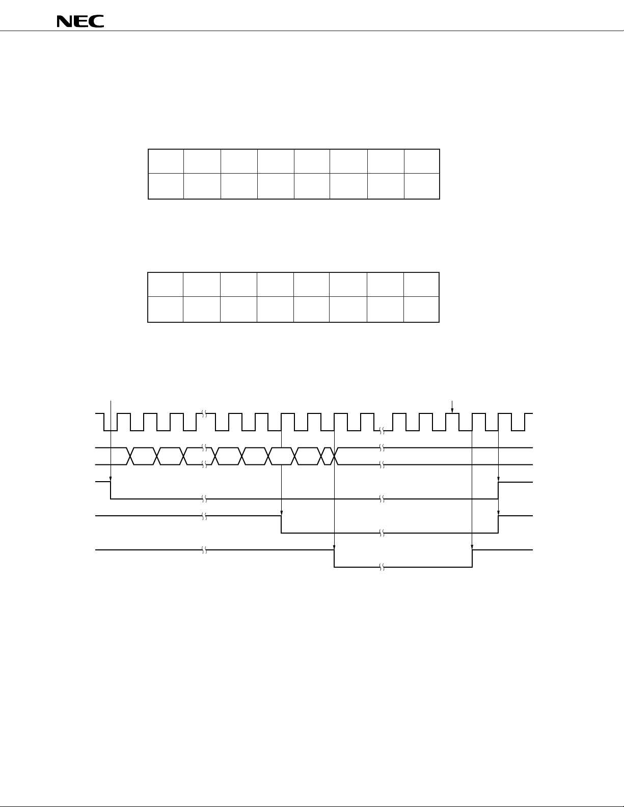
(2) Timer (tone interval) output (TIMER pin)
Outputs rectangular waves of the same pattern as the tone signal interrupt pattern. This is used to make the
LED blink in synchronization with the ringer tone.
Figure 2-4 Digital Accessory Output Waveform
REC10
RAUXO
(Tone output)
RINGER
TIMER
2.1.5 Audio Digital Signal Processor
Send signal digital BPF processing, receive signal digital LPF processing, transmission level (digital gain)
control, and tone generation processing.
(1) Voice send signal digital gain fine adjustment function
Performs gain fine adjustment for voice send signal by digital coefficient multiplication. Together with prefilter
gain adjustment, fine adjustment is possible at a width of 5.8 dB.
(2) Voice receive signal digital gain fine adjustment function
Performs fine adjustment of gain for voice receive signal by digital coefficient multiplication.
(3) Tone generation function
Generates single-tone and dual-tone audible signals. Tone frequency, interrupt pattern, gain, generation/stop
can be controlled by microcontroller command. GSM triple tone can be generated by special command.
11
Page 12
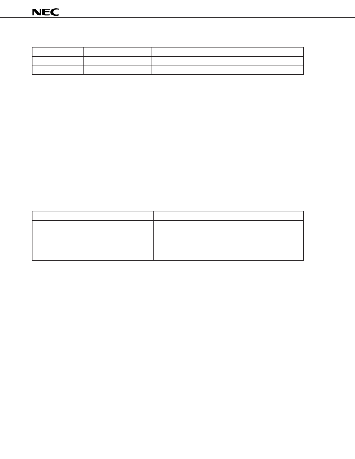
Table 2-3 Digital Gain Control Functions
µ
PD9930
Voice Send Signal Gain Control
Gain setting method Microcontroller command Microcontroller command Microcontroller command
Gain setting range 0 to –2.8 dB (0.4 dB steps) 0 to –2.4 dB (0.8 dB steps) 0 to –30 dB (1 dB steps), –38.5 dB
2.1.6 Power Up/Down Control
The µPD9930 includes a power down function for reducing power consumption. Power down control is by
the two methods described below.
(1) Input/output amplifier power up/down control
Power up/down for both the input and output amplifiers can be controlled.
When the power down function is used for all input amplifiers, both pre-filter and A/D enter the power down state.
When the power down function is used for the accessory output amplifier and the receiver 1 amplifier, the D/A
also enters power down state.
(2) Stand-by mode
Low power consumption can be realized in the mode in which all chip operation is stopped. The stand-by mode
is set by power down command. Operation restarts by power up command.
The following control registers are used to enable the control described above.
Control Method Registers Used
Power up/down control of input/output amplifier Input/output amplifier control register (AMPCR)
(not including receiver amplifier 2)
Power up/down control of receiver amplifier 2 Send analog gain/receiver amplifier 2 control register (TXGCR)
Set/clear of standby mode Power up control command (PUPCMD)
Voice Receive Signal Gain Control
Power down control command (PDWCMD)
Tone Gain Control
An outline diagram of power down control is shown in Figure 2-5.
12
Page 13
Figure 2-5 Power Down Control
µ
PD9930
Register address
0 0 0 MICPDB
XAUXPDB REC1PDB RAUXPDB RINGPDB
Register address
000110
AMPCR
TXGCR
REC2PDB
TXAG
Power up command
011110——
Power down command
011100——
Note M: HEX value with MSB first L: HEX value with LSB first
Stand-by
Pre-filter
+ mixer
When all input amplifiers are
in the power down state,
these also enter power
down state.
A/D
to XACOMI
Microphone input
–
+
"1" = Power ON
Accessory input
–
+
"1" = Power ON
ref
to V
MICPDB
XAUXPDB
ML
78H 1EH
ML
70H 0EH
PLL
Stand-by
Digital signal
processor
HEX
HEX
Note
Note
Accessory output
–
+
"1" = Power ON
Receiver 1
–
+
"1" = Power ON
Receiver 2
Ringer output
–
+
–
+
"1" = Ringer output
to V
to V
RAUXPDB
REC1PDB
ref
ref
RINGPDB
Stand-by
D/A
Stand-by
When both accessory output
and receiver 1 amplifiers are
in the power down state, these
also enter power down state.
Stand-by
"1" = Power ON
REC2PDB
Stand-by
Caution MICPDB and XAUXPDB cannot enter the power up state at the same time (MICPDB = XAUXPDB =
"1").
13
Page 14
µ
PD9930
(3) Input/output amplifier control register (AMPCR)
This is a 5-bit register for power up/down control of each input/output amplifier (not including receiver amplifier
2), and for ringer output ON/OFF control.
Remark For information on power up/down control of receiver amplifier 2, refer to 4.1.1 Voice Send Analog Gain/
Receiver Amplifier 2 Control Register (TXGCR).
Figure 2-6 Input/Output Amplifier Control Register
Register address AMPCR
D7 D6 D5 D4 D3 D2 D1 D0
0 0 0 MICPDB
XAUXPDB REC1PDB RAUXPDB RINGPDB
MICPDB
0
1 Power up
XAUXPDB
0
1 Power up
REC1PDB
0
1 Power up
RAUXPDB
0
1 Power up
Microphone amplifier power control
Power down
Accessory input amplifier power control
Power down
Receiver amplifier 1 power control
Power down
Accessory output amplifier power control
Power down
RINGPDB
Ringer output control
Sets output at low level.
0
1 Output enable
Remarks 1. In the stand-by mode, all amplifiers enter the power down state regardless of input/output control register
settings. However, register contents are held unless reset or written, so when the stand-by mode is
cleared by power up command, the command prior to the stand-by mode is resumed.
2. The microphone and accessory amplifiers cannot enter the power up (D4 = D3 = "1") state at the same
time.
14
Page 15
Table 2-4 Function Specification by Input/Output Amplifier Control Register
µ
PD9930
Register address
D7 D6 D5 D4 D3 D2 D1 D0 M L
00000000 X X X X Stop 00H 00H At reset
AMPCR HEX
00001 X X X X Output 01H 80H
00010 X X X O Stop 02H 40H
00011 X X X O Output 03H C0H
00100 X X O X Stop 04H 20H
00101 X X O X Output 05H A0H
00110 X X O O Stop 06H 60H
00111 X X O O Output 07H E0H
01000 X O X X Stop 08H 10H
01001 X O X X Output 09H 90H
01010 X O X O Stop 0AH 50H
01011 X O X O Output 0BH D0H
01100 X O O X Stop 0CH 30H
01101 X O O X Output 0DH B0H
01110 X O O O Stop 0EH 70H
01111 X O O O Output 0FH F0H
10000 O X X X Stop 10H 08H
10001 O X X X Output 11H 88H
10010 O X X O Stop 12H 48H
10011 O X X O Output 13H C8H
10100 O X O X Stop 14H 28H
10101 O X O X Output 15H A8H
10110 O X O O Stop 16H 68H
10111 O X O O Output 17H E8H
Microphone
amplifier
Accessory
input amplifier
Receiver
amplifier 1
Accessory
output amplifier
Ringer output
Note
Remarks
Note M: HEX value with MSB first
L: HEX value with LSB first
Remark O: Power up X: Power down
15
Page 16
µ
PD9930
(4) Power up/down command (PUPCMD/PDWCMD)
The stand-by mode is set and cleared by the following two special commands. When resetting, the stand-by
mode is set.
Figure 2-7 Power Down Command (Sets to stand-by mode)
D7 D6 D5 D4 D3 D2 D1 D0
PDWCMD
011100XX
Remark X: Don't Care
Figure 2-8 Power Up Command (Clears stand-by mode)
D7 D6 D5 D4 D3 D2 D1 D0
PUPCMD
011110XX
Remark X: Don't Care
Power up/down timing
Power down commandPower up command
FSYNC
COUNT 238 23910 2 3 240 241 0 0
ANAPWD
CLKPWD
DSPPWD
Remarks COUNT: Internal counter (counts with an 8-kHz internal clock)
ANAPWD: Analog power down (power down when high)
CLKPWD: Clock power down (power down when high)
DSPPWD: Signal processing power down (power down when high)
16
Page 17
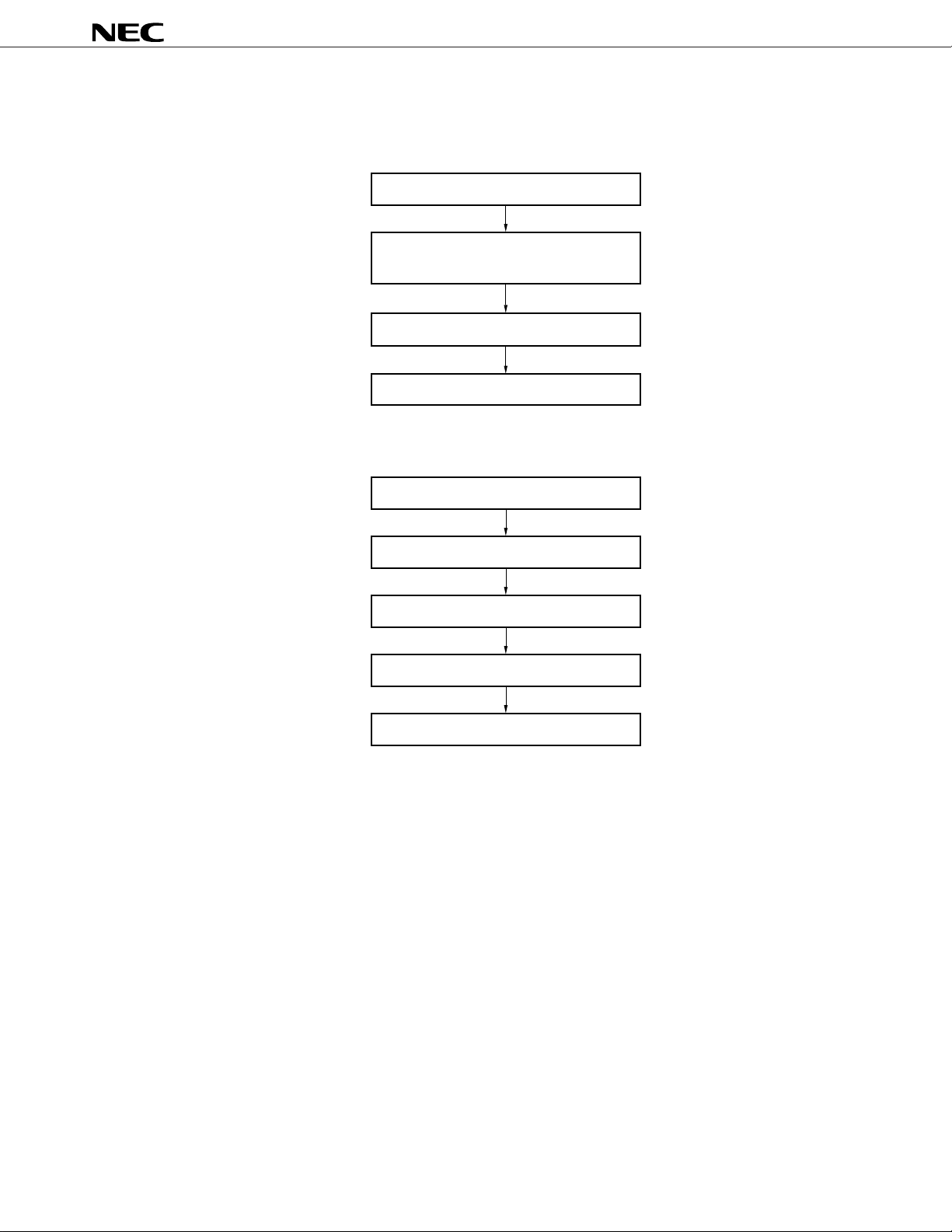
(5) Power up/down sequence
(a) Power down sequence
(b) Power up sequence
Power down command execution
Digital signal processing (filter operation,
tone generation operation) operation stop
Clock (internal clock, serial clock) power down
Analog (PLL, all amplifiers) power down
µ
PD9930
Power up command execution
Analog and PLL operation start
PLL clock stabilization
Clock operation start
Digital signal operation start
Remarks 1. The DSP interface serial input/output operation does not stop or start when switching to power up/down.
2. Rising time from standby mode to normal operation mode is about 30.5 ms after execution of the power
up command.
3. FSYNC can be stopped at power down. However, input of the FSYNC clock is necessary during
operation and in the above sequence.
17
Page 18
µ
PD9930
2.1.7 Microcontroller Interface
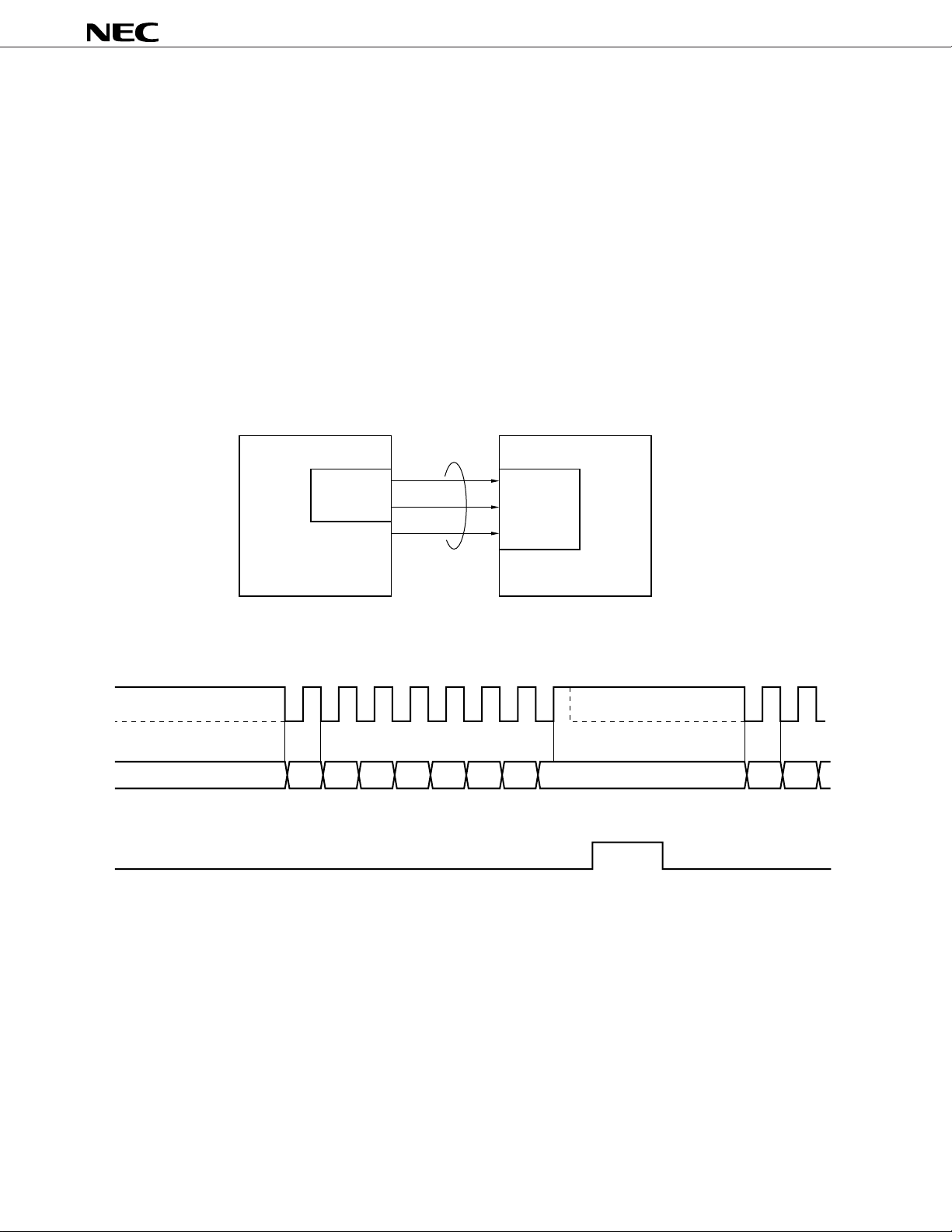
The µPD9930 can control internal functions by microcontroller command. A clock synchronous serial I/O is
incorporated to receive command.
A clocked serial interface is provided to receive microcontroller commands. A microcontroller connection
example is shown in Figure 2-9. 8-bit length data is received by the serial clock (MCLK), serial input (MDAT),
Note
and strobe input (MSTR) lines
.
The timing chart is shown in Figure 2-10. By reading data to the internal shift register and setting MSTR
to high level at the MCLK rising point, it is latched to the internal control register. Data transfer must be made
with LSB first.
Note When 8 bits or more (9 MCLK clocks or more) data is input, the last 8-bit which is input immediately before
the active edge of MSTR is recognized as a control command.
Figure 2-9 Example of Connection with Microcontroller
PD9930
Microcontroller
µ
MCLK
MDAT
MSTR
Serial I/O
SO
SCK
PORT
Microcontroller I/F
MDAT
MCLK
MSTR
Figure 2-10 Microcontroller Interface Timing Chart
D0 D1 D2 D3 D4 D5 D6 D7 D0 D1
18
Page 19

µ
g
PD9930
2.1.8 DSP Interface
A clock synchronous serial I/O is built-in to exchange voice send/receive coding data with an external DSP.
16-bit data is transferred at 8 kHz by the serial clock (SCLK = 256 kHz), serial input (SI), serial output (SO),
and enable output (SEN) lines. The REQB is a terminal for allowing/inhibiting data transmission. There are
two modes for data input and output timing, and either can be selected by the DSPSEL terminal. Select the
mode matching the DSP serial interface input/output timing. Data format is as follows: Both SO output and SI
input are in 2's complement format with MSB first.
Figure 2-11 Data Format in DSP Interface
D15 D14 D13 D12 D11 D10 D9 D8 D7 D6 D5 D4 D3 D2 D1 D0SO output
Coding data (13 bits)
Sign bit Invalid data
Remark A full code is output when the SO pin is +3.17 dBm0 (A/D 1.2 V
D15 D14 D13 D12 D11 D10 D9 D8 D7 D6 D5 D4 D3 D2 D1 D0SI input
Coding data (15 bits)
Si
n bit
p-p).
Remark When a full code is input to the SI pin, the accessory output is 1.2 V
Table 2-5 DSP Input/Output Timing Mode Selection
Pin input
DSPSEL
H MODE1
L MODE2
Mode
Table 2-6 Allowing Data Transmission
REQB pin Input Data Transmission
L Data transmission is allowed. Enable signal (SEN) is output at rising edge of FSYNC (8 kHz), and
data input/output is started.
H Enable signal is not output and data are not input or output.
p-p.
19
Page 20
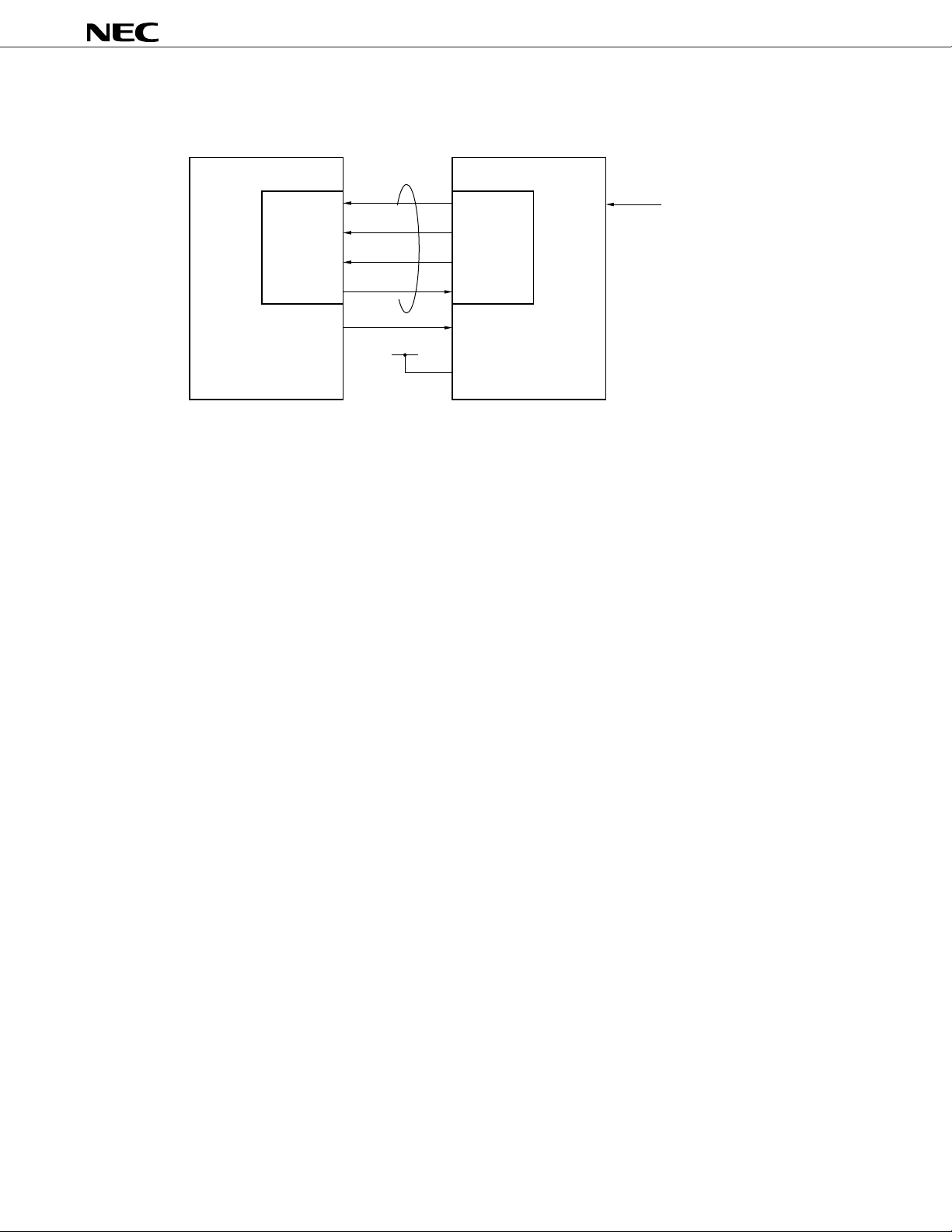
Figure 2-12 Example of Connection with DSP (Mode 1)
µ
DSP
PD9930
µ
PD9930
Serial I/O
SCK
enable
SI
SO
PORT
V
DD
Note When using with mode 2, connect DSPSEL to GND.
DSP I/F
SCLK
SEN
SO
SI
REQB
DSPSEL
Note
FSYNC
8 kHz
20
Page 21
REQB
FSYNC
(8 kHz)
SEN
SCLK
(256 kHz)
SO
SI
125 s
D15 D14 D2 D1 D0 D15 D14
D15 D14 D2 D1 D0 D15 D14D13
D13
µ
D13
D12
don't care don't care
Figure 2-13 DSP Interface Timing Chart
µ
PD9930
REQB
FSYNC
(8 kHz)
SEN
SCLK
(256 kHz)
SO
SI
don't care
(a) Mode 1 (DSPSEL = V
125 s
µ
D15 D14 D2 D1 D0 D15 D14
D15 D14 D2 D1 D0 D15 D14
DD)
don't care
D13
D13
(b) Mode 2 (DSPSEL = GND)
21
Page 22
µ
PD9930
2.1.9 DAI (Digital Audio Interface)
Has a on-chip circuit enabling DAI functions specified in GSM11.10. The receive system has a on-chip LPF
only. If a BPF is necessary, it should be mounted externally. System configuration at the time of DAI test mode
is shown in Figure 2-15. The DAI terminal is connected to the system simulator via the pin 25 DSUB socket.
The test mode can be selected by terminals TC1 or TC2, or by microcontroller command. DAI mode should be
set after completing power-up operation (30.5 ms after executing power-up command).
When changing the modes from DAI to normal, either of the following operations should be executed.
• After specifying normal mode, input the DAI reset signal (DRSTB = low).
• Input reset signal (RESETB = low).
When specifying by command, test control register mode specification bits (ITC1, ITC2) are used (Refer to
4.4.1 Test Control Register (TSTCR).).
Timing for each mode is shown in Figures 2-16 through 2-20.
For operation at the time of each mode, refer to Figure 4-13 Test Mode Operation.
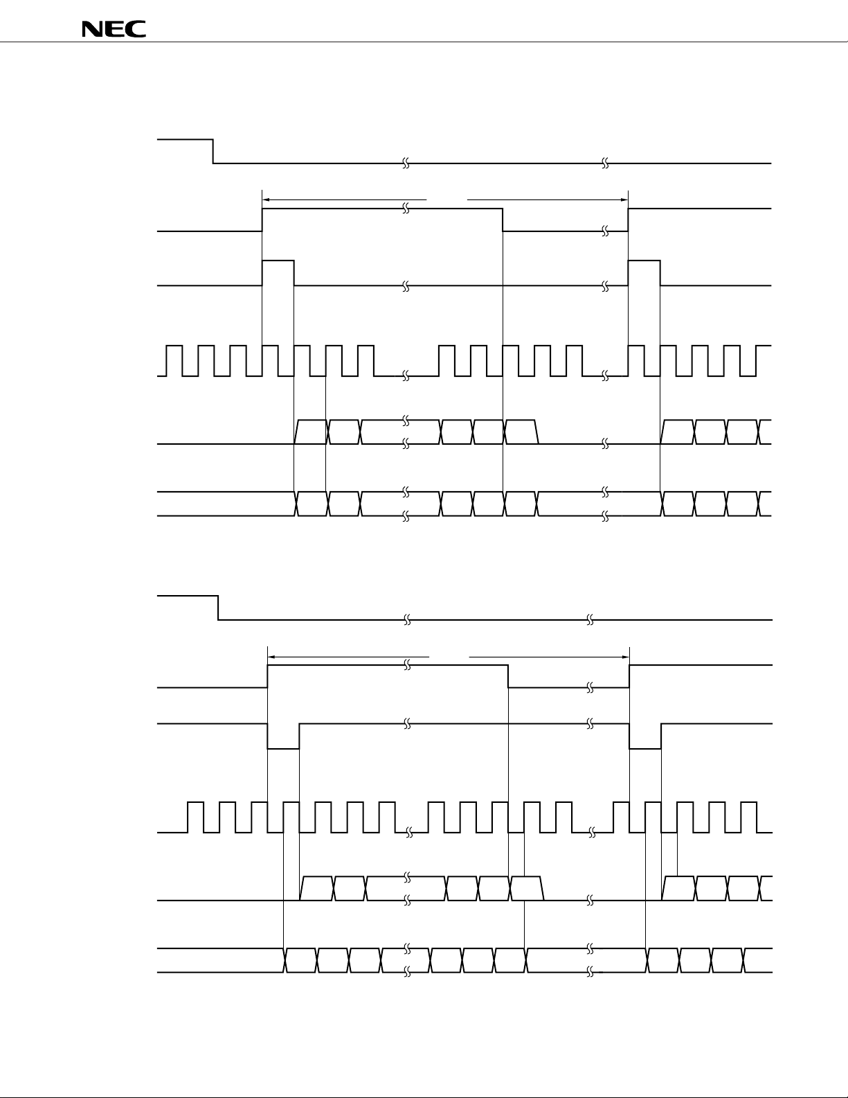
Table 2-7 DAI Test Mode Specification
TC2 TC1 Test mode Function
(ITC2) (ITC1) specification
0 0 Normal operation
0 1 Speech encoder Outputs data input from DI pin to DSP (speech encoder) from SO pin.
test mode Input is started at rising edge of first FSYNC (8-kHz external clock input) after
1 0 Speech decoder Outputs speech decoder output data input from SI pin from DO pin.
test mode Inputting data from DSP is started at rising edge of first FSYNC (8-kHz external
1 1 Acoustic device, A/D, Outputs audio data converted into digital signal from DO pin.
D/A test mode Also inputs audio data input from DI pin to D/A converter. Inputting/outputting data
Note
Normal operation.
This mode is set at system reset (when RESETB = low) regardless of status of TC1
and TC2.
execution of mode specification, and outputting data to DSP is started at next rising
edge of FSYNC.
clock input) after execution of mode specification, and data is output from DO pin at
next rising edge of FSYNC.
is started at rising edge of first FSYNC (8-kHz external clock input) after execution
of mode specification. At this time, clock output to DSP (SCLK) is stopped.
Note In the normal mode, do not set DRSTB to low level (during low period, serial interface with DSP is disabled).
As well, set the output pins of driver IC to high-impedance state, because DRSTB input pin is connected with
a pull-up resistor.
Remark Analog loop back mode and DAI test mode cannot be specified at the same time.
DAI test mode is set with TC1, TC2 (or ITC1, ITC2) and DRSTB pins. DAI test mode is entered at the rising
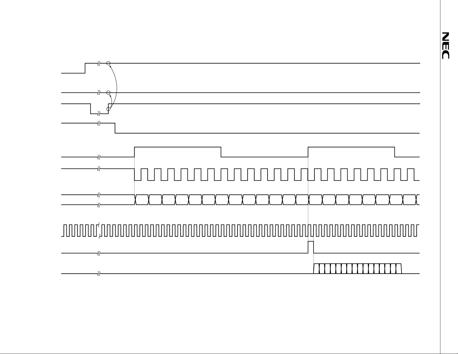
edge of the DRSTB signal when both TC1 and TC2 pins (or ITC1 and ITC2 pins) are set as shown in Figure
2-14.
22
Page 23
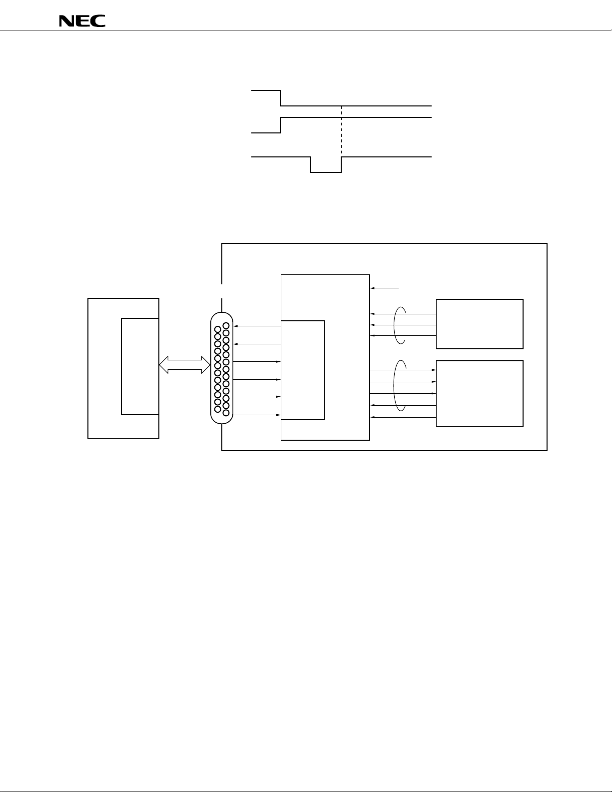
Figure 2-14 Latch Timing of TC1, TC2 (or ITC1, ITC2)
TC1 (ITC1)
TC2 (ITC2)
DRSTB
Figure 2-15 Example of System Configuration at Time of DAI Test Mode
Mobile equipment
PD9930
µ
µ
PD9930
8 kHz
Test command
Microcontroller
DSP
(SP-CODEC)
DAI
25-Pin DSUB socketSystem simulator
DAI
DCLK
DO
DI
TC1
TC2
DRSTB
FSYNC
MCLK
MSTR
MDAT
SCLK
SEN
SO
SI
REQB
Remark In the acoustic device test mode, REQB is ignored (both high and low levels). When DSPSEL = VDD (mode
1), SCLK and SEN are fixed to low, and when DSPSEL = GND (mode 2), fixed to high.
23
Page 24
24
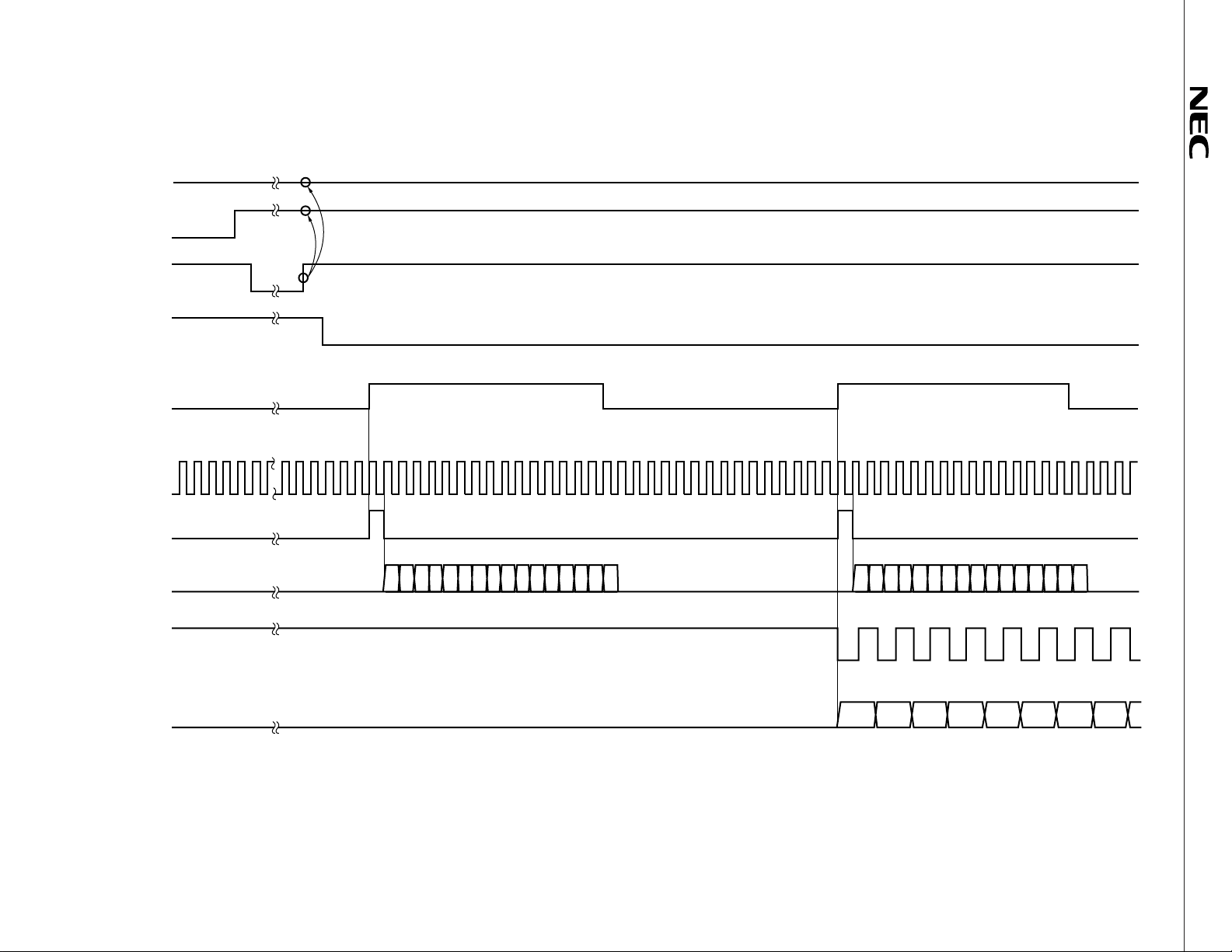
Figure 2-16 Speech Encoder Test Mode (DSP Interface = MODE 1) (TC1 = 1, TC2 = 0)
TC1 (ITC1)
TC2 (ITC2)
DRSTB
REQB
FSYNC
(8 kHz)
DCLK
(104 kHz)
DI
SCLK
(256 kHz)
SEN
don't care
"L"
D12 D11 D10 D9 D8 D7 D6 D5 D4 D3 D2 D1 D0 D12 D11 D10 D9 D8 D7 D6 D5
SO
D14 D13 D12 D11 D10 D9 D8 D7 D6 D5 D4 D3 D2 D1 D0
D15
µ
PD9930
Page 25

TC1 (ITC1)
Figure 2-17 Speech Encoder Test Mode (DSP Interface = Mode 2) (TC1 = 1, TC2 = 0)
TC2 (ITC2)
DRSTB
REQB
FSYNC
(8 kHz)
DCLK
(104 kHz)
DI
SCLK
(256 kHz)
don't care
"L"
D12 D11 D10 D9 D8 D7 D6 D5 D4 D3 D2 D1 D0 D12 D11 D10 D9 D8 D7 D6 D5
25
SEN
SO
D14 D13 D12 D11 D10 D9 D8 D7 D6 D5 D4 D3 D2 D1 D0
D15
µ
PD9930
Page 26
26
Figure 2-18 Speech Decoder Test Mode (DSP Interface = Mode 1) (TC1 = 0, TC2 = 1)
TC1 (ITC1)
TC2 (ITC2)
DRSTB
REQB
FSYNC
(8 kHz)
SCLK
(256 kHz)
SEN
SI
D15
"L"
D0D1D2
D10D11D12D13D14
D3D4D5D6D7D8D9
D15
D10D11D12D13D14
D0D1D2
D3D4D5D6D7D8D9
DCLK
(104 kHz)
DO
D12 D11 D10 D9 D8 D7 D6 D5
µ
PD9930
Page 27

Figure 2-19 Speech Decoder Test Mode (DSP Interface = Mode 2) (TC1 = 0, TC2 = 1)
TC1 (ITC1)
TC2 (ITC2)
DRSTB
REQB
FSYNC
(8 kHz)
SCLK
(256 kHz)
SEN
"L"
SI
D15
D10D11D12D13D14
D0D1D2
D3D4D5D6D7D8D9
D15
D10D11D12D13D14
D0D1D2
D3D4D5D6D7D8D9
27
DCLK
(104 kHz)
DO
D12 D11 D10 D9 D8 D7 D6 D5
µ
PD9930
Page 28

28
Figure 2-20 Acoustic Device Test Mode (DSP Interface = Mode 1) (TC1 = 1, TC2 = 1)
TC1 (ITC1)
TC2 (ITC2)
DRSTB
REQB
FSYNC
(8 kHz)
SCLK
(256 kHz)
DCLK
(104 kHz)
DI
DO
D12 D11 D10 D9 D8 D7 D6 D5 D4 D3 D2 D1 D0 D12 D11 D10 D9 D8 D7 D6 D5
D12 D11 D10 D9 D8 D7 D6 D5 D4 D3 D2 D1 D0 D12 D11 D10 D9 D8 D7 D6 D5
Note In DSP Interface = Mode 2, SCLK is fixed to high.
Note
µ
PD9930
Page 29

µ
PD9930
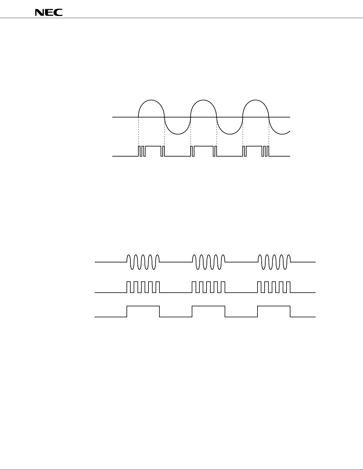
3. TONE INTERVAL OUTPUT FUNCTION (TIMER TERMINAL)
When a tone is generated, an interval signal that indicates the tone intermittent state is output. The function
is used, for example, to make the LED blink in synchronization with the ringer tone.
Figure 3-1 Tone Interval Output Waveform
Tone generation
(1) Continuous tone
(2) Intermittent tone
(when 31.25 ms on/off)
(3) One-shot tone
(200 ms one-shot)
(4) GSM triple tone
Tone generation
(31.25 ms)
Tone generation
Tone generation
Tone stop
(31.25 ms)
(200 ms)
Tone stop
(1 s)
(1 s)
29
Page 30

µ
PD9930
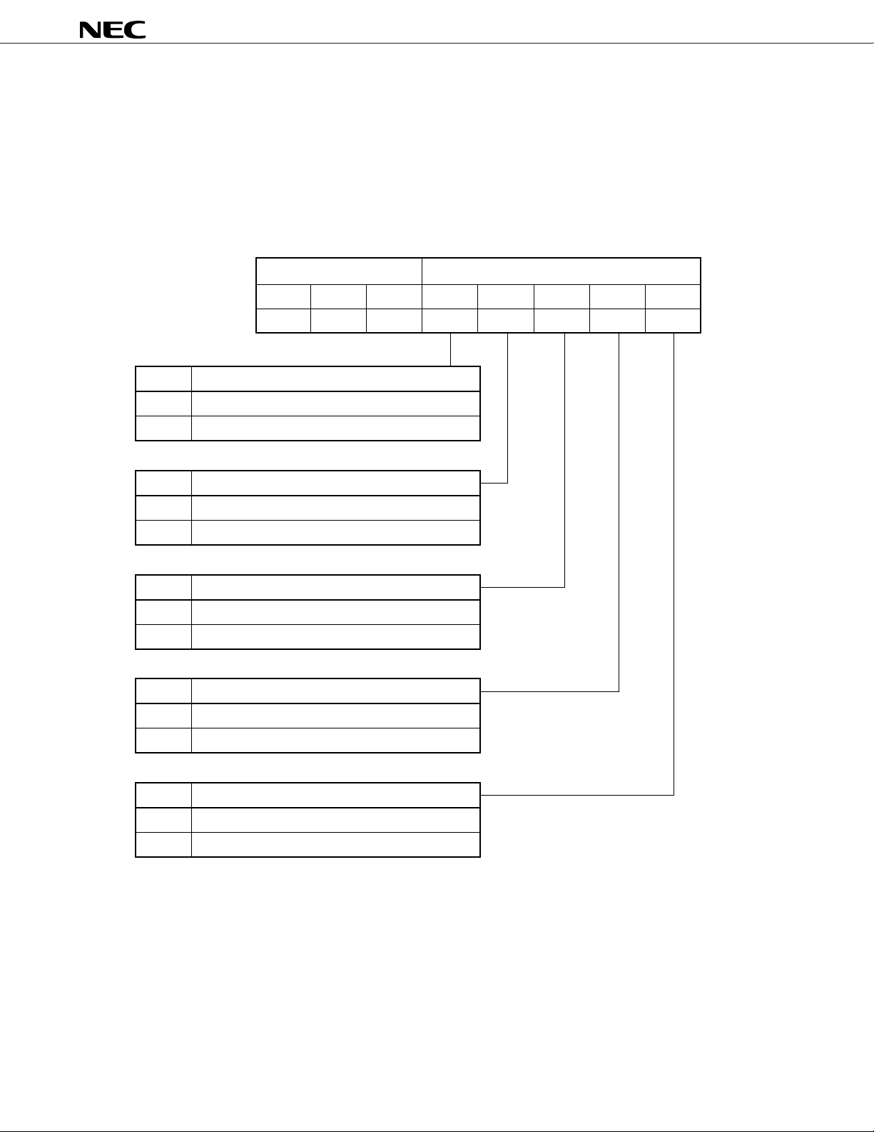
4. INTERNAL CONTROL FUNCTIONS
The µPD9930 can control internal functions by commands from a microcontroller. Commands consist of 8bit data (D7 to D0) consisting of register address and setting data, and are written in the following internal
registers.
Register name Control
(1) Voice send analog gain/receiver amplifier 2 control register (TXGCR) Voice send/receive gain control
(2) Voice receive analog gain control register (RXGCR)
(3) Voice send/receive digital gain control register (DGGSR)
(4) Digital signal processing control register (DSPCR) Digital input/output control
(5) Tone frequency selection register (FRQSR) Tone control
(6) Expanded tone register (EXPR1/EXPR2)
(7) Tone control register (TONCR)
(8) Tone gain control register (TNGCR)
(9) Input/output amplifier control register (AMPCR) Power up/down control
(10) Power up control command (PUPCMD)
(11) Power down control command (PDWCMD)
(12) Test control register (TSTCR) Test mode control
Remarks 1. In the case of registers (1), (2), and (9) to (11), written contents are executed instantly.
µ
2. For registers (3) to (8) and (12), since fetch execution is made by the internal clock (125
s interval),
keep 125 µs or more interval for write-in to the same register.
If the write-in to the same register is executed continuously, the previous command may be ignored.
3. Even when in the stand-by mode, write-in to each internal register is possible (can be held), but the
command written in the register is executed only after clearing the stand-by mode.
4.1 SEND/RECEIVE GAIN CONTROL
An outline of send/receive gain control is shown in Figure 4-1.
µ
With the
Voice send gain Pre-filter analog gain adjustment Voice send analog gain/receiver amplifier 2
control (0, –3 dB) control register (TXGCR)
Voice receive gain Receiver amplifier 1 analog gain adjustment Voice receive analog gain control register
control (volume control) (0 to –31 dB, 1 dB steps) (RXGCR)
PD9930, the following send and receive gain control is possible.
Send/receive gain control Register used
Digital gain fine adjustment Voice send/receive digital gain control register
(0 to –2.8 dB, 0.4 dB steps) (DGGSR)
Digital gain fine adjustment Voice send/receive digital gain control register
(0 to –2.4 dB, 0.8 dB steps) (DGGSR)
30
Page 31

Figure 4-1 Send/Receive Gain Control
µ
PD9930
Register address
000110
Pre-filter/mixer
Microphone input
or
Accessory input
Receiver output
Voice send analog
gain control
0, –3 dB
010
Receiver amplifier 1
Voice receive analog
gain control
TXGCR
REC2PDB
A/D
Register address
D/A
TXAG
Digital signal-processor
0 to –2.8 dB
(0.4 dB steps)
Voice send digital
gain control
DGGSR
RXDG1 RXDG0 TXDG2 TXDG1 TXDG0
LPF
Voice receive digital
BPF
gain control
SO
SI
0 to –31 dB
(1 dB steps)
Register address
001
RXAG4 RXAG3 RXAG2 RXAG1 RXAG0
0 to –2.4 dB
(0.8 dB steps)
RXGCR
31
Page 32

µ
PD9930
4.1.1 Voice Send Analog Gain/Receiver Amplifier 2 Control Register (TXGCR)
This register controls pre-filter gain. It also controls receiver amplifier 2 power up/down as shown in Table
4-1 (Refer to 2.1.6 Power Up/Down Control).
When power is down, the contents of the register area retained. After power is up, control continues as before
power was down.
Figure 4-2 Voice Send Analog Gain/Receiver Amplifier 2 Control Register
REC2PDB
0
1
TXAG
0
1
Register address
D7 D6 D5 D4 D3 D2 D1 D0
0 0 0 1 1 0 REC2PDB TXAG
Receiver amplifier 2 power up/down specification
Power down
Power up
Pre-filter analog gain specification
Sets to 0 dB
Sets to –3 dB
TXGCR
Table 4-1 Function Specification by Send Analog Gain/Receiver Amplifier 2 Control Register
Register address TXGCR HEX
D7 D6 D5 D4 D3 D2 D1 D0 M L
00011000 Power down 0 dB 18H 18H At reset
0 0 1 Power down –3 dB 19H 98H
0 1 0 Power up 0 dB 1AH 58H
0 1 1 Power up –3 dB 1BH D8H
Receiver amplifier 2 Voice send analog gain Remarks
Note
Note M: HEX value with MSB first
L: HEX value with LSB first
32
Page 33

4.1.2 Voice Receive Analog Gain Control Register (RXGCR)
This is a 5-bit register for controlling the analog gain (volume) of receiver amplifier 1.
Figure 4-3 Voice Receive Analog Gain Control Register
Register address RXGCR
D7 D6 D5 D4 D3 D2 D1 D0
0 0 1 RXAG4 RXAG3 RXAG2 RXAG1 RXAG0
µ
PD9930
RXAG4 to RXAG0
00000 to 11111
Receiver amplifier 1 gain specification
0 to –31 dB (1 dB steps)
33
Page 34

µ
Table 4-2 Function Specifications by Voice Receive Analog Gain Control Register
PD9930
Register address
D7 D6 D5 D4 D3 D2 D1 D0 M L
00100000 0 dB 20H04H
RXGCR HEX
Voice receive analog gain Remarks
00001 –1 dB 21H84H
00010 –2 dB 22H44H
00011 –3 dB 23HC4H
00100 –4 dB 24H24H
00101 –5 dB 25HA4H
00110 –6 dB 26H64H
00111 –7 dB 27HE4H
01000 –8 dB 28H14H
01001 –9 dB 29H94H
01010 –10 dB 2AH 54H
01011 –11 dB 2BH D4H
01100 –12 dB 2CH 34H
01101 –13 dB 2DH B4H
01110 –14 dB 2EH 74H
01111 –15 dB 2FH F4H
10000 –16 dB 30H 0CH
10001 –17 dB 31H 8CH
10010 –18 dB 32H 4CH
10011 –19 dB 33H CCH
10100 –20 dB 34H 2CH
10101 –21 dB 35H ACH
10110 –22 dB 36H 6CH
10111 –23 dB 37H ECH
11000 –24 dB 38H 1CH
11001 –25 dB 39H 9CH
11010 –26 dB 3AH 5CH
11011 –27 dB 3BH DCH
11100 –28 dB 3CH 3CH
11101 –29 dB 3DH BCH
11110 –30 dB 3EH 7CH
11111 –31 dB 3FH FCH At reset
Note
Note M: HEX value with MSB first
L: HEX value with LSB first
34
Page 35

µ
PD9930
4.1.3 Voice Send/Receive Digital Gain Control Register (DGGSR)
This is a 5-bit register for adjusting the gain of the digital signal processor. The gain of the send system and
receive system can be fine-adjusted independently.
Figure 4-4 Send/Receive Digital Gain Control Register
RXDG1 to RXDG0
00 to 11
TXDG2 to TXDG0
000 to 111
Register address
D7 D6 D5
010
Receive digital gain specification
0 to –2.4 dB (0.8 dB steps)
Send digital gain specification
0 to –2.8 dB (0.4 dB steps)
D4 D3
RXDG1
DGGSR
D2 D1 D0
RXDG0 TXDG2 TXDG1 TXDG0
35
Page 36

µ
PD9930
Table 4-3 Function Specifications by Voice Send/Receive Digital Gain Control Register
Register address
D7 D6 D5 D4 D3 D2 D1 D0 M L
01000000 0 dB 0 dB 40H02HAt reset
DGGSR HEX
00001 0 dB –0.4 dB 41H 82H
00010 0 dB –0.8 dB 42H 42H
00011 0 dB –1.2 dB 43H C2H
00100 0 dB –1.6 dB 44H 22H
00101 0 dB –2.0 dB 45H A2H
00110 0 dB –2.4 dB 46H 62H
00111 0 dB –2.8 dB 47H E2H
01000 –0.8 dB 0 dB 48H 12H
01001 –0.8 dB –0.4 dB 49H 92H
01010 –0.8 dB –0.8 dB 4AH 52H
01011 –0.8 dB –1.2 dB 4BH D2H
01100 –0.8 dB –1.6 dB 4CH 32H
01101 –0.8 dB –2.0 dB 4DH B2H
01110 –0.8 dB –2.4 dB 4EH 72H
01111 –0.8 dB –2.8 dB 4FH F2H
10000 –1.6 dB 0 dB 50H 0AH
10001 –1.6 dB –0.4 dB 51H 8AH
10010 –1.6 dB –0.8 dB 52H 4AH
10011 –1.6 dB –1.2 dB 53H CAH
10100 –1.6 dB –1.6 dB 54H 2AH
10101 –1.6 dB –2.0 dB 55H AAH
10110 –1.6 dB –2.4 dB 56H 6AH
10111 –1.6 dB –2.8 dB 57H EAH
11000 –2.4 dB 0 dB 58H 1AH
11001 –2.4 dB –0.4 dB 59H 9AH
11010 –2.4 dB –0.8 dB 5AH 5AH
11011 –2.4 dB –1.2 dB 5BH DAH
11100 –2.4 dB –1.6 dB 5CH 3AH
11101 –2.4 dB –2.0 dB 5DH BAH
11110 –2.4 dB –2.4 dB 5EH 7AH
11111 –2.4 dB –2.8 dB 5FH FAH
Voice receive Voice send
digital gain digital gain
Note
Remarks
Note M: HEX value with MSB first
L: HEX value with LSB first
36
Page 37

µ
PD9930
4.2 DIGITAL INPUT/OUTPUT CONTROL
An outline of digital input/output control is shown in Figure 4-5.
µ
PD9930 can control input and output of the digital signal processor as follows.
The
Digital input/output control Registers used
Voice send data BPF operation processing execution/stop
Connection and disconnection to tone output Voice send/ Digital signal processing control register
receive system (DSPCR)
Serial output terminal (SO) control
Serial input terminal (SI) control
Caution You must not connect nor disconnect tone output voice send/receive system in the tone operation.
It causes malfunction.
Figure 4-5 Digital Input/Output Control
A/D
D/A
Register address
0110
TXACT
1 = ON
Note
TNACT
1 = ON
TXACT TNACT SOACT SIACT
Digital signal processor
BPF
LPF
Tone
generator
DSPCR
DSP I/F
DGND
DGND
SOACT
1
0
SIACT
SO
1
0
SI
Note Connected when TXACT = 0 and TNACT = 1.
37
Page 38

4.2.1 Digital Signal Processing Control Register (DSPCR)
This is a 4-bit register for controlling digital signal processor input/output.
Figure 4-6 Digital Signal Processing Control Register
Register address DSPCR
D7 D6 D5 D4 D3 D2 D1
0 1 1 0 TXACT TNACT SOACT SIACT
µ
PD9930
D0
TXACT
TNACT
SOACT
SIACT
Voice send data processing control
0
Stops voice send data digital BPF processing.
Executes voice send data digital BPF processing.
1
Tone output control
0
Disconnects tone output from voice send/receive systems.
Connects tone output to voice send/receive systems.
1
DSP interface output control
Note
Note
.
.
0
Sets serial output (SO) at low level
Outputs send data (or tone data) to the serial output (SO).
1
DSP interface input control
0
Sets serial input (SI) at low level
Inputs receive data to serial input (SI).
1
Note Test Control Register can set serial input/output terminal at low level, too (refer to 4.4.1 Test Control Register
(TSTCR)).
Caution Before specification of SOACT bit, be sure to write "0" for SIOOFF bit of Test Control Register.
If "0" isn't written for SIOOFF bit, serial output terminal is set at low level, regardless of SOACT bit.
38
Page 39

Table 4-4 Function Specification by Digital Signal Processing Control Register
µ
PD9930
Register address DSPCR HEX
D7 D6 D5 D4 D3 D2 D1 D0 M L
01100000 Note 2 Note 3 60H 06H At reset
0001 Note 2 Voice receive signal output 61H 86H
0010 Inhibiting command — —
0011 Inhibiting command — —
0100 Note 2 Tone output 64H 26H
0101 Note 2
0110 Tone output Tone output 66H 66H
0111 Tone output
1000 Inhibiting command — —
1001 Inhibiting command — —
1010 Voice send signal output Note 3 6AH 56H
1011 Voice send signal output Voice receive signal output 6BH D6H
1100 Inhibiting command — —
1101 Inhibiting command — —
1110 Voice send signal output Tone output 6EH 76H
1111 Voice send signal output
Serial output control Control of output to D/A Remarks
Voice receive signal + tone outpu
Voice receive signal + tone output
Voice receive signal + tone output
Note
t 65H A6H
67H E6H
6FH F6H
Notes 1. M: HEX value with MSB first
L: HEX value with LSB first
2. Stops voice send data processing and serial output.
3. Stops voice receive data serial input and tone output.
39
Page 40

µ
PD9930
4.3 TONE CONTROL
An outline diagram of the tone generator is shown in Figure 4-7. Tone generation is by the tone 1 oscillation
circuit and the tone 2 oscillation circuit.
The tone 1 oscillation circuit generates high group frequency for DTMF and four types of single tones (tone
1 frequency).
The tone 2 oscillation circuit generates low group frequency (tone 2 frequency) for DTMF. Dual tone is output
by adding tone 1 frequency.
In addition to registered tones, other frequencies can be registered. Also, GSM triple tone can be generated
by special command. Examples of tone generation are shown in Figure 4-8.
Tone control items are shown below.
Tone control Registers used
Tone frequency Registered tone Specification of DTMF Tone frequency selection register
Single tone: 400 Hz, 425 Hz, 2 kHz, 2.6 kHz (FRQSR)
Selection of GSM triple tone Tone control register (TONCR)
User registration Registration of desired tone in 0.3 to 3.4 kHz Tone frequency selection register
tone range. (FRQSR)
(Single tone, dual tone) Expanded tone register 1
(EXPR1)
Expanded tone register 2
(EXPR2)
Generation pattern Registered 31.25 ms intermittence, 200 ms intermittence, Tone control register
pattern 250 ms intermittence, 500 ms intermittence, (TONCR)
1s intermittence, 200 ms one-shot tone
Desired pattern Interrupted at desired interval by START/STOP
command
Gain Control of tone output gain Tone gain control register
0 to –30 dB (1 dB steps), –38.5 dB (TNGCR)
40
Page 41

Figure 4-7 Tone Control
Expanded tone register 1
Expanded tone register 2
Register address
100
Tone 1 oscillation circuit
Tone 1 frequency
1209 Hz 400 Hz
1336 Hz 425 Hz
1477 Hz 2000 Hz
1633 Hz 2600 Hz
Expanded tone 1 frequency
START/
STOP
Tone 2 oscillation circuit
Tone 2 frequency
697 Hz 770 Hz
852 Hz 941 Hz
Expanded tone 2 frequency
FRQSEL4 FRQSEL3 FRQSEL2 FRQSEL1 FRQSEL0
3.1 dBm0
3.1 dBm0
FRQSR
Register address
111
–6 dB
Tone interval
– ∞ dB
0
1
–9 dB
generation
TNGAIN4
0 to –30 dB
(1-dB steps)
–38.5 dB
TNGAIN3
TNACT
TNGCR
TNGAIN2 TNGAIN1 TNGAIN0
LPF output (receive signal)
Note
(Only sign code)
Note Digital signal processing control
register bit 2 (Refer to Figure 4-6).
Ringer output
To D/A
Serial output
Timer output
41
Register address
01 1 TNMODE TNP2 TNP1 TNP0
TONCR
µ
PD9930
START/
STOP
Page 42

µ
PD9930
Figure 4-8 Tone Generation Examples
(a) When generating a busy tone (b) When generating DTMF "7" with continuous tone
(400 Hz single tone, 500 ms intermittence)
Busy tone generation
Tone gain control register
Set tone gain.
Tone frequency selection register
Set frequency to 400 Hz.
Tone control register
Select single tone
Select 500 ms intermittent pattern.
START/STOP = "1" (start)
END
DTMF "7" generation
Tone gain control register
Set tone gain.
Tone frequency selection register
Set frequency to DTMF "7".
Tone control register
Select dual tone.
Select continuous tone.
START/STOP = "1" (start)
END
(c) When generating GSM triple tone (d) When generating 200 ms intermittent user regis-
ter tone (480 Hz single tone; coefficient =
0111011100B)
GSM triple tone generation
Tone gain control register
Set tone gain.
Tone control register
Select single tone
Select GSM triple tone
START/STOP = "1" (start)
END
User register tone generation
Tone gein control register
Set tone gain.
Tone frequency selection register
Specify "user register"
Expanded tone register 1
"100110" (registration command) +
registration data
(lower order 2 bits) setting
Expanded tone register 1
Registration data
(higher-order 8 bits) setting
Tone control register
Select single tone.
Select 200 ms intermittent pattern.
START/STOP = "1" (start)
42
END
Page 43

µ
PD9930
4.3.1 Tone Frequency Selection Register (FRQSR)
This is a 5-bit register for specifying tone 1 (high group frequency for DTMF and four types of single tones)
and tone 2 (low group frequency for DTMF) frequency combinations.
Figure 4-9 Tone Frequency Selection Register
Register address FRQSR
D7 D6 D5
1 0 0 FRQSEL4
D4 D3 D2 D1 D0
FRQSEL3 FRQSEL2 FRQSEL1 FRQSEL0
FRQSEL4 to FRQSEL0
00000 to 10100
Write operation in this register is instantaneously executed and retained when a command is received, but
change of tone generation or generating tone is executed only when "1" is written for START/STOP control bit
of the tone control register (refer to Figure 4-11 Tone Control Register).
When a user registration tone is selected, the tone specified by the expanded tone register (refer to Figure
4-10 Expanded Tone Frequency Registration Procedure) is generated.
Caution Do not input a command that sets a tone oscillation frequency after inputting a tone oscillation
command (writing "1" to the START/STOP control bit of the tone control register).
Tone frequency selection
Refer to Table 4-5 Function Specification by Tone Frequency Selection Register.
43
Page 44
Table 4-5 Function Specification by Tone Frequency Selection Register
µ
PD9930
Register address
D7 D6 D5 D4 D3 D2 D1 D0 M L
10000000 DTMF “1” 1209 Hz 697 Hz 80H 01H
FRQSR HEX
00001 DTMF “2” 1336 Hz 697 Hz 81H 81H
00010 DTMF “3” 1477 Hz 697 Hz 82H 41H
00011 DTMF “A” 1633 Hz 697 Hz 83H C1H
00100 DTMF “4” 1209 Hz 770 Hz 84H 21H
00101 DTMF “5” 1336 Hz 770 Hz 85H A1H
00110 DTMF “6” 1477 Hz 770 Hz 86H 61H
00111 DTMF “B” 1633 Hz 770 Hz 87H E1H
01000 DTMF “7” 1209 Hz 852 Hz 88H 11H
01001 DTMF “8” 1336 Hz 852 Hz 89H 91H
01010 DTMF “9” 1477 Hz 852 Hz 8AH 51H
01011 DTMF “C” 1633 Hz 852 Hz 8BH D1H
01100 DTMF “∗” 1209 Hz 941 Hz 8CH 31H
01101 DTMF “0” 1336 Hz 941 Hz 8DH B1H
01110 DTMF “#” 1477 Hz 941 Hz 8EH 71H
01111 DTMF “D” 1633 Hz 941 Hz 8FH F1H
10000 400 Hz
10001 425 Hz
10010 2 kHz
10011 2.6 kHz
10100 User registration User registration 94H 29H
10101 Inhibiting command — —
10110 Inhibiting command — —
10111 Inhibiting command — —
DTMF function Tone 1 frequency Tone 2 frequency Remarks
Note 2
Note 2
Note 2
Note 2
Indefinite value 90H 09H
Indefinite value 91H 89H
Indefinite value 92H 49H
Indefinite value 93H C9H At reset
Note 1
Notes 1. M: HEX value with MSB first
L: HEX value with LSB first
2. This is single tone. When specifying this tone, be sure to specify the tone control register in the single tone
mode (refer to Figure 4-11 Tone Control Register).
Remark For DTMF tone generation, specify the tone control register in the dual tone mode (refer to Figure 4-11
Tone Control Register). If the register is specified in the single tone mode, only the high group tone (tone
1 frequency) is generated.
44
Page 45

µ
PD9930
4.3.2 Expanded Tone Registers (EXPR1, EXPR2)
(1) Expanded Tone Frequency Registration Procedure
µ
PD9930 can register desired tone frequencies (expanded tone frequencies) in 0.3 to 3.4 kHz range.
The
Expanded tone register 1 (EXPR1) is for registering expanded tone 1 frequency (high group frequency for DTMF
and single tone). Expanded tone register 2 (EXPR2) is for registering expanded tone 2 frequency (low frequency
for DTMF). The frequency must be specified by 10-bit coefficient (2's complement).
Registration of single tone is done with EXPR1 (single-tone generation is impossible by EXPR2) (refer to Figure
4-10 (a)).
When registering dual tone, set high group in EXPR1 and low group in EXPR2.
Write operation in this register can be executed by continuously writing the expanded tone registration command
and expanded tone data command (refer to Figure 4-10).
Once registered, the frequency is valid until reset or updated.
Figure 4-10 Expanded Tone Frequency Registration Procedure
(a) Expanded tone 1 frequency registration procedure
<1> Set expanded tone 1 registration command in EXPR1.
Expanded tone 1 registration command
EXPR1
<2> Set higher-order 8 bits of expanded tone coefficient (expanded tone 1 data command) in EXPR1.
EXPR1
Remark EA9 to EA0: Tone 1 frequency 10-bit coefficient
<1> Set expanded tone 2 registration command in EXPR2.
EXPR2
<2> Set higher-order 8 bits of expanded tone coefficient (expanded tone 2 data command) in EXPR2.
D7 D6 D5 D4 D3 D2 D1 D0
100110EA1EA0
Expanded tone 1 data command
D7 D6 D5 D4 D3 D2 D1 D0
EA9 EA8 EA7 EA6 EA5 EA4 EA3 EA2
(b) Expanded tone 2 frequency registration procedure
Expanded tone 2 registration command
D7 D6 D5 D4 D3 D2 D1 D0
100111EB1EB0
Expanded tone 2 data command
EXPR2
Remark EB9 to EB0: Tone 2 frequency 10-bit coefficient
Caution After executing the expanded tone registration command, the next command is written as expanded
tone data, so continuously execute the expanded tone data command.
D7 D6 D5 D4 D3 D2 D1 D0
EB9 EB8 EB7 EB6 EB5 EB4 EB3 EB2
45
Page 46

µ
PD9930
(2) Expanded Tone Data Determination Method
The coefficient E of the tone frequency fe (0.3 to 3.4 kHz) to be generated is determined by the following formula.
π
E = COS (2
Coefficient E: Sign bit 1 bit + 9 bits below the decimal point (Coefficient: 2's complement)
Example When specifying 400 Hz single tone
COS (2
Next, the least significant bit is determined.
fe/fs) fs = 8 kHz
π
x 400/8000) = COS (π x 0.1)
= COS (0.3141592653......)
= 0.951056516......
= (0.11110011X) b (Higher-order 9 bits are determined.)
When (0.11110011
When (0.111100111) b = 0.951071875
Since fe" is nearest to 400 Hz, the coefficient to be registered is (0.111100111) b = (1E7) H.
0111100111
↓↓↓↓↓↓↓↓↓↓
EA9 EA8 EA7 EA6 EA5 EA4 EA3 EA2 EA1 EA0
The error of oscillation frequency by rounding 10-bit coefficient is below ±5 Hz (MAX. at 300 Hz → ±1.7 %) for
all frequencies.
About ±1.67 % near 300 Hz (±5 Hz)
About ±1.00 % near 500 Hz (±5 Hz)
About ±0.40 % near 1 kHz (±5 Hz)
About ±0.25 % near 2 kHz (±5 Hz)
About ±0.16 % near 3 kHz (±5 Hz)
0) b = 0.94921875
2π fe' x fs = COS–1 (0.94921875) = 0.320052983
π
fe' = 0.320052983 x fs/(2
fe' = 407.504115
π
fe" x fs = COS–1 (0.951071875) = 0.314109559
2
fe" = 0.314109559 x fs/(2π)
fe" = 399.524415
)
Coefficient is negative number in fe > 2.0 kHz.
46
Page 47

µ
PD9930
4.3.3 Tone Control Register (TONCR)
This is a 5-bit register for controlling single tone/dual tone specification, generation pattern selection, and
generation and stopping.
Figure 4-11 Tone Control Register
TNMODE
0
1
TNP2
0
0
0
0
1
1
1
1
D7 D6
1
Single tone/dual tone specification
Single tone mode
Dual tone mode
TNP1
TNP0
Generation pattern selection
0
0
Continuous tone generation
0
1
1
0
0
1
1
31.25 ms tone, 31.25 ms no tone repeated
1
200 ms tone, 200 ms no tone repeated
0
250 ms tone, 250 ms no tone repeated
1
500 ms tone, 500 ms no tone repeated
0
1
1 s tone, 1s no tone repeated
0
GSM triple tone generated
200 ms interval tone generated (one shot tone)
1
Register address
0
Remarks
At reset
Note 1
TONCR
D5 D4 D3 D2 D1 D0
1 TNMODE
TNP2
Remarks
At reset
TNP1
TNP0
START
/STOP
START/STOP
0
1
Tone generation/stop control
Stop ("1" → "0", "0" → "0" both valid)
Validation of tone ferquency selection register setting data, start of
generation ("1"→ "1", "0" → "1" both valid)
Note 2
Remarks
At reset
Notes 1. 950 Hz tone 333 ms, 1400 Hz tone 333 ms, 1800 Hz tone 333 ms, 1 s no tone repeated.
2. Do not input a command that sets a tone oscillation frequency after inputting a tone oscillation command
(writing "1" to the START/STOP control bit of the tone control register).
Remark When the regeneration pattern is specified as "110", it becomes GSM triple tone command, so tone
generation forcibly enters single tone mode.
Tone generation and change of a tone that is being generated is executed only when "1" is written for START/
STOP control bit (D0 bit) (refer to Figure 4-11 and Table 4-6).
47
Page 48

Table 4-6 Function Specification by Tone Control Register
µ
PD9930
Register address
D7 D6 D5 D4 D3 D2 D1 D0 ML
101XXXX0Tone stop A0H 05H
TONCR HEX
Tone control conditions
00001Continuous single tone generation A1H 85H
0001131.25 ms intermittent single tone generation A3H C5H
00101200 ms intermittent single tone generation A5H A5H
00111250 ms intermittent single tone generation A7H E5H
01001500 ms intermittent single tone generation A9H 95H
010111 s intermittent single tone generation ABH D5H
01101GSM triple tone generation ADH B5H
01111200 ms one-shot single tone generation AFH F5H
10001Continuous dual tone generation B1H 8DH
1001131.25 ms intermittent dual tone generation B3H CDH
10101200 ms intermittent dual tone generation B5H ADH
10111250 ms intermittent dual tone generation B7H EDH
11001500 ms intermittent dual tone generation B9H 9DH
110111 s intermittent dual tone generation BDH BDH
11111200 ms one-shot dual tone generation BFH FDH
Note
Note M: HEX value with MSB first L: HEX value with LSB first
Remark X: Don't care
4.3.4 Tone Gain Control Register (TNGCR)
This is a 5-bit register for controlling the tone output gain.
Figure 4-12 Tone Gain Control Register
Register address TNGCR
D7 D6 D5 D4 D3 D2 D1 D0
1 1 1 TNGAIN4 TNGAIN3 TNGAIN2 TNGAIN1 TNGAIN0
TNGAIN4 to TNGAIN0
00000 to 11111
Tone gain selection (Refer to Table 4-7 Function
Specification by Tone Gain Control Register).
0 to –30 dB (1 dB steps), –38.5 dB
48
Page 49

Table 4-7 Function Specification by Tone Gain Control Register
µ
PD9930
Register address
D7 D6 D5 D4 D3 D2 D1 D0 M L
11100000 0 dB E0H07H
TNGCR HEX
Tone gain Remarks
00001 –1 dB E1H87H
00010 –2 dB E2H47H
00011 –3 dB E3HC7H
00100 –4 dB E4H27H
00101 –5 dB E5HA7H
00110 –6 dB E6H67H
00111 –7 dB E7HE7H
01000 –8 dB E8H17H
01001 –9 dB E9H97H
01010 –10 dB EAH 57H
01011 –11 dB EBH D7H
01100 –12 dB ECH 37H
01101 –13 dB EDH B7H
01110 –14 dB EEH 77H
01111 –15 dB EFH F7H
10000 –16 dB F0H 0FH
10001 –17 dB F1H 8FH
10010 –18 dB F2H 4FH
10011 –19 dB F3H CFH
10100 –20 dB F4H 2FH At reset
10101 –21 dB F5H AFH
10110 –22 dB F6H 6FH
10111 –23 dB F7H EFH
11000 –24 dB F8H 1FH
11001 –25 dB F9H 9FH
11010 –26 dB FAH 5FH
11011 –27 dB FBH DFH
11100 –28 dB FCH 3FH
11101 –29 dB FDH BFH
11110 –30 dB FEH 7FH
11111 –38.5 dB FFH FFH
Note
Note M: HEX value with MSB first
L: HEX value with LSB first
49
Page 50
µ
PD9930
4.4 TEST MODE CONTROL
The µPD9930 has the following test functions.
Test function Registers used
DAI test function This test function is stipulated in GSM11.10. Test mode selection can be Test control
controlled by external terminal (TC1 or TC2) or internal register (ITC1, register (TSTCR)
ITC2).
Analog loopback function Send data after BPF processing is input to LPF.
DSP interface input/ SO, SI, SCLK and SEN terminals can be set at low level.
output control function
An outline of test mode control is shown in Figure 4-13.
50
Page 51

Mobile Station
PD9930
µ
DSP I/F
DSP
TX
SO
DAI
speech
encoder
DI
TC1
TC2
1
0
System
simulator
Mobile Station
PD9930
µ
DSP I/F
DSP
RX
SI
DAI
speech
decoder
DO
TC1
TC2
1
0
System
simulator
Mobile Station
PD9930
µ
A/D
D/A
BPF
LPF
DAI
DO
DI
TC1
TC2
1
1
A/D
D/A
BPF
LPF
PD9930
µ
(a) DAI (speech encoder test mode) (b) DAI (speech decoder test mode)
(c) DAI (A/D, D/A test mode) (d) Analog loopback mode
System
simulator
Figure 4-13 Test Mode Operation
µ
PD9930
51
Page 52

µ
PD9930
4.4.1 Test Control Register (TSTCR)
This is a 5-bit control register for selecting the test mode.
ITC1, ITC2 become valid at the rising edge of DRSTB. For the precautions when using DAI, refer to 2.1.9
DAI (Digital Audio Interface).
Figure 4-14 Test Control Register
Register address TSTCR
D7 D6 D5 D4 D3 D2 D1 D0
1 1 0 TCMODE
ITC2 ITC1
LOOPBK SIOOFF
TCMODE
ITC2
0
0 Speech encoder test mode
1
1
LOOPBK
SIOOFF
DAI test mode control method selection
Specification of test mode by external terminals TC1 and TC2
0
1
Specification of test mode by test control registers ITC1 and ITC2
DAI test mode specification
ITC1
0
Normal operation
1
0
Speech decoder test mode
1
Acoustic device, A/D, D/A test mode
Analog loopback specification
Normal operation
0
1 Analog loopback
DSP interface input/output terminal control
Normal operation
0
1
Setting of terminals SO, SI, SCLK, and SEN to low level
Remarks
At reset
Remarks
At reset
Remarks
At reset
Remarks
At reset
Remark The analog loopback mode and the DAI test mode cannot be specified at the same time.
52
Page 53

µ
PD9930
5. ELECTRICAL CHARACTERISTICS
ABSOLUTE MAXIMUM RATINGS (TA = 25˚C, DGND = AGND1 to AGND4 = 0 V)
Item Symbol Conditions Ratings Unit
Supply Voltage VDD AVDD1, AVDD2, DVDD –0.3 to +5.5 V
Analog Input Voltage VAIN All analog input pins –0.3 to VDD +0.3 V
Digital Input Voltage VDIN All digital input pins –0.3 to VDD +0.3 V
Analog Output Pin Applied Voltage VAOUT All analog output pins –0.3 to VDD +0.3 V
Digital Output Pin Applied Voltage VDOUT All digital output pins –0.3 to VDD +0.3 V
Operating Ambient Temperature TA –30 to +85 ˚C
Storage Temperature Tstg –65 to +150 ˚C
Cautions 1. Connect the AGND1 through AGND4 pins and DGND pin to an analog ground line near µPD9930
pins. Connect the DVDD, AVDD1, AVDD2 pins to an analog power supply line near µPD9930 pins.
2. Do not connect output (and bidirectional) pins each other. Do not connect output (or bidirectional) pins directly to the V
pin can be directly connected to VDD, VCC, or GND line. If timing design is made so that no signal
conflict occurs, three-state pins can also be connected directly to three-state pins of external
circuit.
3. Exposure to Absolute Maximum Ratings for extended periods may affect device reliability;
exceeding the ratings could cause permanent damage. The parameters apply independently.
The device should be operated within the limits specified under DC and AC Characteristics.
DD, VCC, or GND line. However, open drain pin and open collector
53
Page 54

µ
PD9930
RECOMMENDED OPERATING RANGE (TA = –30 to +85˚C)
(1) DC Condition
Item Symbol Conditions MIN. TYP. MAX. Unit
Supply Voltage VDD AVDD1, AVDD2, DVDD 2.7 3.0 3.6 V
High Level Input Voltage VIH All digital input pins 0.7 VDD VDD V
Low Level Input Voltage VIL All digital input pins 0 0.3 VDD V
Analog Input Voltage VIA All analog input pins 0.6 1.8 V
Microphone Input
Analog Input Voltage VMIC Differential: MICI+, MICI– 1.2 Vp-p
Gain Setting Range GMIC Set with external resistor 15 33 dB
Load Resistance RLMIC Includes gain setting resistance 50 kΩ
Load Capacitance CLMIC 20 pF
Accessory Input
Analog Input Voltage VAUXI XAUXI– 1.2 Vp-p
Gain Setting Range GAUXI Set with external resistor 0 10 dB
Load Resistance RLAUXI Includes gain setting resistance 300 kΩ
Load Capacitance CLAUXI 20 pF
Pre-filter + Mixer Input
Analog Input Voltage VMIXI MIXI 1.2 Vp-p
Accessory Output
Load Resistance RLAUXO 100 kΩ
Load Capacitance CLAUXO 100 pF
Receiver 1 Output
Load Resistance RLREC1 100 kΩ
Load Capacitance CLREC1 20 pF
Receiver 2 Output
Analog Input Voltage VREC2 REC2I- 1.2 Vp-p
Gain Setting Range GREC2 Set with external resistor – ∞ +10 dB
Load Resistance RLREC2 60 nF series 2 kΩ
Load Capacitance CLREC2 2 kΩ series 60 nF
Reference Voltage Output
Load Capacitance CLACOM XACOMO, RACOMO 0.2 10
µ
F
(2) Frame Signal (FSYNC) and Reset Signal (RESETB)
Item Symbol Conditions MIN. TYP. MAX. Unit
FSYNC Frequency fs 7.995 8.000 8.005 kHz
FSYNC High Level Width tWHS 2.0
FSYNC Low Level Width tWLS 2.0
FSYNC Rise Time tr 20 ns
FSYNC Fall Time tf 20 ns
RESETB Low Level Width tRSL 260 ns
54
µ
s
µ
s
Page 55

µ
PD9930
(3) Microcontroller Interface
Item Symbol Conditions MIN. TYP. MAX. Unit
MCLK Cycle Time tMCY 240 ns
MCLK High Level Width tMCH 100 ns
MCLK Low Level Width tMCL 100 ns
MCLK Rise Time tMR 20 ns
MCLK Fall Time tMF 20 ns
MDAT Setup Time to tSUMDA 50 ns
MSTR ↑
MDAT Hold Time from tHMDA 50 ns
MCLK ↑
MSTR High Level Width tWMST 320 ns
MCLK Setup Time to tSUMCK 0ns
MSTR ↑
MSTR Setup Time to t SUMST 100 ns
MCLK ↑
(4) DSP Interface
Item Symbol Conditions MIN. TYP. MAX. Unit
SI Setup Time to SCLK ↓ tSUSI 200 ns
SI Hold Time from SCLK ↓ tHSI 200 ns
(5) DAI
Item Symbol Conditions MIN. TYP. MAX. Unit
DI Setup Time to DCLK ↑ tSUDI 200 ns
DI Hold Time from DCLK ↑ tHDI 200 ns
TC1, TC2 Rise Time tTR 50 ns
TC1, TC2 Fall Time tTF 50 ns
DRSTB Low Level Width tDRSL 130
DRSTB Rise Time tDRR 20 ns
DRSTB Fall Time tDRF 20 ns
DAI Mode Setting Time 1 tTCF 60 ms
DAI Mode Setting Time 2 tTCR 260
REQB Low Level Width tDRQL 130
REQB High Level Width t DRQH 130
REQB Rise Time tDRQR 20 ns
REQB Fall Time tDRQF 20 ns
µ
s
µ
s
µ
s
µ
s
55
Page 56

µ
PD9930
CAPACITANCE (TA = 25˚C)
Item Symbol Conditions MIN. TYP. MAX. Unit
Digital Output Pin COD f = 1 MHz 20 pF
Capacitance
Digital Input Pin CID f = 1 MHz 20 pF
Capacitance
DC CHARACTERISTICS (TA = 25˚C, V DD = 2.7 to 3.6 V (GND standard))
(1) Current Consumption
Item Symbol Conditions MIN. TYP. MAX. Unit
Circuit Current in Normal IDD1 Microphone input 7.0 9.0 mA
Mode (1020 Hz: –10 dBm0)
Accessory input: Power down
serial input (1020 Hz: –10 dBm0)
Accessory output: Power up
Receiver 1, 2: Power up
Circuit Current in DAI IDD2 Microphone input 7.5 10.0 mA
Operation (1020 Hz: –10 dBm0)
Accessory input: Power down
serial input (1020 Hz: –10 dBm0)
Accessory output: Power up
Receiver 1, 2: Power up
Circuit Current in Standby IDD3 DI, DRSTB, TC1, TC2: Open 50 100
Mode FSYNC: 8 kHz
Other digital input pins: 0 or VDD
(2) Digital Part
Item Symbol Conditions MIN. TYP. MAX. Unit
Digital Input Leak Current ILH VI = VDD 1.0
ILL VI = 0 –1.0
Pull-Up/Down Current IIL VDD = 3.3 V, 0 ≤ VI ≤ VDD 100
Low Level Output Voltage VOL IOL = 2.0 mA 0.4 V
High Level Output Voltage VOH IOH = –2.0 mA 2.4 V
µ
A
µ
A
µ
A
µ
A
56
Page 57

µ
(3) Analog Part
Item Symbol Conditions MIN. TYP. MAX. Unit
Pre-filter + Mixer
Volume Range GPRF –3 0 dB
Volume Accuracy ∆GPRF Volume 0 dB standard –3.2 –3.0 –2.8 dB
Cross-Talk 1 between CTIN1 Microphone input amplifier: Power down –45 dB
Input Channels MICI = 1.2 Vp-p
XAUXI– = 0 Vp-p
Accessory input gain setting: 0 dB
Cross-Talk 2 between CTIN2 Accessory input amplifier: Power down –45 dB
Input Channels MICI = 0 Vp-p
XAUXI– = 1.2 Vp-p
Accessory input gain setting: 0 dB
Accessory Output
Maximum Output VAMAX 1.2 Vp-p
Voltage
Receiver 1 Output
Maximum Output VR1MAX 1.2 Vp-p
Voltage
Volume Range GREC1 –31 0 dB
Volume Accuracy ∆GREC1 Volume: 0 to –16 dB –1.5 –1.0 –0.5 dB
Note
Volume
Receiver 2 Output
Maximum Output VR2MAX Distortion factor 4 % (MAX.) 4 Vp-p
Voltage
Reference Voltage Output
Output Voltage VACOM XACOMO, RACOMO 1.2 V
: –17 to –31 dB –2.0 –1.0 0.0 dB
PD9930
Note Simple decrease in the gain due to drop of volume is guaranteed.
(4) Tone Generator
Item Symbol Conditions MIN. TYP. MAX. Unit
Output Signal Level VTN1 Tone 1 –2.93 –2.73 dBm0
VTN2 Tone 2 –5.93 –5.73
Frequency Deviation ∆FTN 0.3 to 3.4 kHz –5 +5 Hz
Distortion Factor TNSD Accessory output 30 dB
Tone Volume Range GTN –38.5 0 dB
Tone Volume Accuracy ∆GTN Volume: 0 to –30 dB (1 dB steps) –1.4 –1.0 –0.8 dB
57
Page 58

AC CHARACTERISTICS
µ
PD9930
(1) DSP Interface (T
Item Symbol Conditions MIN. TYP. MAX. Unit
SCLK Cycle Time tSCY 3906 ns
SCLK High Level Width tSCH 1953 ns
SCLK Low Level Width tSCL 1953 ns
SCLK Rise Time tSR 20 ns
SCLK Fall Time tSF 20 ns
SCLK Delay Time from tDSCLK 1.0
FSYNC ↑
SEN ↑ Delay Time from tDSENR 80 ns
FSYNC ↑
SEN ↓ Delay Time from tDSENF 80 ns
SCLK ↑: Mode 1
SEN ↓ Delay Time from
SCLK ↓: Mode 2
SO Output Delay Time tDSO 40 ns
from SCLK ↑: Mode 1
SO Output Delay Time
from SCLK ↓: Mode 2
A = –30 to +85˚C, V DD = 2.7 to 3.6 V, CL = 100 pF)
µ
s
(2) DAI (TA = –30 to +85˚C, V DD = 2.7 to 3.6 V, CL = 100 pF)
Item Symbol Conditions MIN. TYP. MAX. Unit
DCLK Cycle Time tDCY 9615 ns
DCLK High Level Width tDCH 4808 ns
DCLK Low Level Width tDCL 4808 ns
DCLK Rise Time tDR 20 ns
DCLK Fall Time tDF 20 ns
DCLK Delay Time from tDDCLK 200 ns
FSYNC ↑
DO Output Delay Time tDDO 200 ns
from DCLK ↓
(3) Others (Digital Output) (TA = –30 to +85˚C, V DD = 2.7 to 3.6 V, CL = 100 pF)
Item Symbol Conditions MIN. TYP. MAX. Unit
TIMER/RINGER Rise Time tDDR TIMER pin and RINGER pin 50 ns
TIMER/RINGER Fall Time tDDF TIMER pin and RINGER pin 50 ns
58
Page 59

Frame signal (FSYNC)
µ
PD9930
1/fs t
WHS
t
r
FSYNC
t
t
f
WLS
Remark During normal operation or the power up/down sequence, be sure to input the frame signal.
Reset signal (RESETB)
RESETB
t
RSL
Remarks 1. The reset signal is input as it is without shaping, so take full precautions against noise.
2. A power on reset circuit is not incorporated, so be sure to set RESET to low after turning the power on.
Microcontroller interface timing
MSTR
t
t
MCY
MCH
MCLK
t
MR
t
SUMDAtHMDA
MDAT
D0 D1 D2 D6 D7 D0
Remark D0 to D7: Microcontroller command (LSB first)
t
MCL
t
SUMCK
WMST
t
t
SUMST
t
MF
59
Page 60

DSP interface timing (mode 1)
SCLK
FSYNC
SEN
t
DSCLK
t
DSENR
t
SCY
t
DSENF
t
DSO
µ
PD9930
t
SCL
t
SFtSCH
t
SR
SO
SI
don't care D15 D14 D13 D0
DSP interface timing (mode 2)
SCLK
FSYNC
SEN
DSCLK
t
t
DSENF
D15 D14 D13 D1 D0
t
SUSItHSI
t
SCY
t
DSENR
t
SCH
t
SRtSCL
don't care
t
SF
60
SO
t
DSO
D15 D14 D13 D1 D0
t
SUSItHSI
SI
don't care
D15 D14 D13
D0
don't care
Page 61

DAI input timing
FSYNC
DCLK
t
DDCLK
t
SUDItHDI
t
DCY
µ
PD9930
t
DCH
t
DCL
t
DF
t
DR
DI
D12 D11 D10 D9 D8 D7
Remark D12 to D0: Input data (MSB first)
DAI output timing
FSYNC
DDCLK
t
DCLK
t
DDO
DO
D12 D11 D10 D9 D8 D7
t
DCY
t
DCL
t
DCH
t
DF
t
DR
Remark D12 to D0: Output data (MSB first)
61
Page 62

TC1, TC2, DRSTB input timing
TC1, TC2
µ
PD9930
t
TR
DRSTB
TIMER, RINGER output timing
TIMER,
RINGER
REQB input timing
t
DDR
TCF
t
t
DRF
t
DRSL
t
DRR
t
TCR
tTR, t
t
TF
DDF
, t
TF
REQB
t
DRQF
t
DRQL
t
DRQR
t
DRQH
62
Page 63

µ
PD9930
TRANSMISSION CHARACTERISTICS
Transmission characteristics are as indicated below unless otherwise specified.
• Analog input
Analog input signal (–10 dBm0, 1020 Hz) → accessory input part
Accessory input: Set gain 0 dB
Microphone input: Power down
Pre-filter + mixer: Set gain 0 dB
• Analog output
Analog output signal → accessory output part
Receiver output: Power down
• Digital gain set
Send and receive: 0 dB
• Digital input signal level: 0 dBm0
A = 25˚C, V DD = 2.7 to 3.6 V (GND standard)
•T
(1) Send/Receive Zero Transmission Level (0 dBm0 level)
Item Symbol Conditions MIN. TYP. MAX. Unit
Send Zero Transmission V0TLPX 600 Ω standard –8.4 dBm
Level
Receive Zero Transmission V0TLPR 600 Ω standard –8.4 dBm
Level
(2) Gain Characteristics
Item Symbol Conditions MIN. TYP. MAX. Unit
Send Gain Deviation GX –0.5 +0.5 dB
Receive Gain Deviation GR –0.5 +0.5 dB
Send Gain Deviation ∆GX –0.4 +0.4 dB
Temperature Power
Fluctuation
Receive Gain Deviation ∆GR –0.4 +0.4 dB
Temperature Power
Fluctuation
(3) Transmission Loss Level
Item Symbol Conditions MIN. TYP. MAX. Unit
Send Transmission Loss GTX +3 to –40 dBm0 –0.4 +0.4 dB
Level
Receive Transmission Loss GTR +3 to –40 dBm0 –0.4 +0.4 dB
Level
–40 to –50 dBm0 –0.6 +0.6 dB
–50 to –55 dBm0 –1.2 +1.2 dB
–40 to –50 dBm0 –0.6 +0.6 dB
–50 to –55 dBm0 –1.2 +1.2 dB
63
Page 64

µ
PD9930
(4) Transmission Gain Frequency Characteristics
Item Symbol Conditions MIN. TYP. MAX. Unit
Send Transmission Gain GRX1 60 Hz –23 dB
Frequency Characteristics
Receive Transmission Gain GRR3 0.3 to 3.0 kHz –0.3 +0.3 dB
Frequency Characteristics
GRX2 200 Hz –2.5 0 dB
GRX3 0.3 to 3.0 kHz –0.3 +0.3 dB
GRX4 3.2 kHz –0.65 +0.3 dB
GRX5 3.4 kHz –0.8 0 dB
GRX6 4.0 kHz –14 dB
GRX7 4.6 kHz or more –28 dB
GRR4 3.2 kHz –0.65 +0.3 dB
GRR5 3.4 kHz –0.8 0 dB
GRR6 4.0 kHz –14 dB
GRR7 4.6 kHz or more –28 dB
(5) Noise Characteristics
Item Symbol Conditions MIN. TYP. MAX. Unit
Send Noise NXC Microphone power down, XAUXI– → 25 dBrnc0
ACOM, gain 0 dB, C message filter
Receive Noise NRC1 C message filter, input +0 code from SI 25 dBrnc0
Single Frequency Noise NSF Send input → Receive output –50 dBm0
Cross-Talk between Send CTTR No sidetone pass, microphone power down –60 dB
and Receive Channels input 0 dBm0 and 1020 Hz from XAUXI–
input +0 code from SI
Cross-Talk between Receive CTRT No sidetone pass, microphone power down –60 dB
and Send Channels XAUXI– → ACOM
input 0 dBm0 and 1020 Hz from SI
Power Supply Voltage PSRR VDD ±100 mV 0-p signal application 30 dB
Variation Rejection f = 0 to 3.4 kHz
–65 dBm0c
–65 dBm0c
64
Page 65

µ
012345678910111213141516
–75
–70
–65
–60
–55
–50
–45
–40
–35
–30
–25
–20
–15
–10
–5
0
5
Frequency (kHz)
Send transmission gain (dB)
PD9930
(6) Distortion Factor Characteristics
Item Symbol Conditions MIN. TYP. MAX. Unit
Send Channel Total Power SDX 0 to –10 dBm0 35 dB
Distortion Factor
Receive Channel Total SDR 0 to –10 dBm0 35 dB
Power Distortion Factor
Absolute Delay DA XAUXI– → RAUXO 550
Delay Distortion Frequency DO XAUXI– → RAUXO 500 Hz 1.40 ms
Characteristics
–40 dBm0 25
–45 dBm0 20
–40 dBm0 25
–45 dBm0 20
600 Hz 0.70
1 kHz 0.20
2.6 kHz 0.20
2.8 kHz 1.40
µ
s
Send Transmission Gain Frequency Characteristics 1 (GRX)
65
Page 66

)
0.1
)
0
–0.1
–0.2
–0.3
–0.4
–0.5
Send transmission gain (dB)
–0.6
Send Transmission Gain Frequency Characteristics 2 (GRX)
µ
PD9930
–0.7
–0.8
–0.9
–5
–10
–15
–20
–25
–30
–35
0
0.2 0.4 0.6 0.8 1.0 1.2 1.4 1.6 1.8 2.0 2.2 2.4 2.6 2.8 3.0 3.2 3.4 3.6 3.8 4.0
Frequency (kHz
Receive Transmission Gain Frequency Characteristics 1 (GRR)
5
0
–40
–45
–50
Receive transmission gain (dB)
–55
–60
–65
–70
–75
012345678910111213141516
66
Frequency (kHz
Page 67

)
Receive Transmission Gain Frequency Characteristics 2 (GRR)
0.1
0
–0.1
–0.2
–0.3
–0.4
–0.5
Receive transmission gain (dB)
–0.6
µ
PD9930
–0.7
–0.8
–0.9
0
0.2 0.4 0.6 0.8 1.0 1.2 1.4 1.6 1.8 2.0 2.2 2.4 2.6 2.8 3.0 3.2 3.4 3.6 3.8 4.0
Frequency (kHz
67
Page 68

µ
Send/receive zero transmission level (0 dBm0 level) is explained below for your reference.
(a) Send zero transmission level
Analog output signal level at which the digital input signal level of the D/A converter becomes 0 dBm0.
(b) Receive zero transmission level
Analog input signal level at which the digital output signal level of the A/D converter becomes 0 dBm0.
(c) Analog signal level (dBm)
The conversion expression of the amplitude voltage of a signal and an analog signal level is as follows:
X = 10 logW
X: analog signal level (dBm)
W: analog signal power (mW)
W = (V
2
/R) x 10
3
V: effective value of analog signal (AC) (Vrms)
R: resistance (Ω)
PD9930
µ
With the
PD9930, the signal voltage (effective value) can be calculated if R = 600 Ω and X = –8.4 dBm are
substituted.
W = 0.1445 (mW)
V = 0.294 (Vrms)
To calculate V
0-p, multiply the signal voltage (effective value) by √2.
0-p = 0.416 (V)
V
(d) Digital signal level (dBm0)
Signal level where the level of the full swing of the digital output value of the A/D converter and the digital input
value of the D/A converter is considered to be 3.17 dBm0 (the amplitude of the analog signal is 1.2 V
the gain of the microphone input or accessory input is 0 dB).
<Level diagram>
This diagram indicates the range in which adjustments can be made by using each amplifier and gain control
function.
Example: Input level at which digital output of linear codec is –10 dBm0 is –33 dBm.
(Conditions)
Microphone amplifier gain during microphone input: 15 dB
Analog gain control: 0 dB
Digital gain control: 0 dB
p-p where
Output level at which digital input of linear codec is –10 dBm0 is –18.4 dBm.
(Conditions)
During receiver output
Analog gain control: 0 dB
Digital gain control: 0 dB
68
Page 69

Voice send level diagram (microphone input)
µ
PD9930
[dBm]
–10
–20
–30
–40
–50
–60
0
+
Vref
–
15 to 33 dB 0 dB or –3 dB 0 to –2.8 dB
–33.4 dBm
–41.4 dBm
Analog
gain control
A/D
Digital
gain control
(0.4 dB steps)
–10 dBm0
–15.8 dBm0
[dBm0]
0
–10
–20
–30
–40
–50
–60
Remarks 1. Thick line: Indicates case where gain of microphone amplifier is set to 15 dB, gain of analog gain control
to 0 dB, and gain of digital gain control to 0 dB.
Thin line: Indicates case where gain of microphone amplifier is set to 33 dB, gain of analog gain control
to –3 dB, and gain of digital gain control to –2.8 dB.
2. Overload level: 3.17 dBm0.
69
Page 70

Voice receive level diagram (receiver output)
µ
PD9930
[dBm]
–10
–20
–30
–40
–50
–60
0
–18.4 dBm
–51.8 dBm
Receiver 1
0 to –31 dB (1 dB steps) 0 to –2.4 dB
Analog
gain control
D/A
Digital
gain control
(0.8 dB steps)
–10 dBm0
[dBm0]
0
–10
–20
–30
–40
–50
–60
Remarks 1. Thick line: Indicates case where gain of analog gain control is set to 0 dB and gain of digital gain control
to 0 dB.
Thin line: Indicates case where gain of analog gain control is set to –31 dB and gain of digital gain
control to –2.4 dB.
2. Overload level: 3.17 dBm0.
70
Page 71

Voice send level diagram (accessory input)
µ
PD9930
[dBm]
–10
–20
–30
–40
–50
–60
0
Vref
0 to 10 dB 0 dB or –3 dB 0 to –2.8 dB
–18.4 dBm
–28.4 dBm
+
–
Analog
gain control
A/D
Digital
gain control
(0.4 dB steps)
–10 dBm0
–15.8 dBm0
[dBm0]
0
–10
–20
–30
–40
–50
–60
Remarks 1. Thick line: Indicates case where gain of microphone amplifier is set to 0 dB, gain of analog gain control
to 0 dB, and gain of digital gain control to 0 dB.
Thin line: Indicates case where gain of microphone amplifier is set to 10 dB, gain of analog gain control
to –3 dB, and gain of digital gain control to –2.8 dB.
2. Overload level: 3.17 dBm0.
71
Page 72

Voice receive level diagram (accessory output)
µ
PD9930
Digital
gain control
(0.8 dB steps)
–10 dBm0
[dBm]
–10
–20
–30
–40
–50
–60
0
–18.4 dBm
–20.8 dBm
Accessory
output
0 dB (fix) 0 to –2.4 dB
D/A
Remarks 1. Thick line: Indicates case where gain of digital gain control is set to 0 dB.
Thin line: Indicates case where gain of digital gain control is set to –2.4 dB.
2. Overload level: 3.17 dBm0.
[dBm0]
0
–10
–20
–30
–40
–50
–60
72
Page 73

1 F 1 F
12 kΩ
100 kΩ to 500 kΩ
0.1 F
300 kΩ
100 kΩ
to 300 kΩ
Accessory
input
2.2 F
+
–
0.1 F
0.1 F
+
–
2.2 F
Note
100 kΩ to 900 kΩ
0.1 F
100 kΩ to
300 kΩ
300 kΩ
0.1 F
Accessory output
+
–
+
–
4.7 F 4.7 F 0.1 F
DSP To REQB
Micro-
controller
DSUB
socket
(25 pin)
V (mode 1)
or GND (mode 2)
DD
From DSP
From
RESET
circuit
8 kHz
1
2
3
4
5
6
7
8
9
10
11
1213141516171819202122
23
24
25
26
27
28
29
30
31
32
33
34 35 36 37 38 39 40 41 42 43 44
MIXI
XAUXO
XAUXI–
XACOMI
XACOMO
RACOMO
RACOMI
REC2O+
REC2O–
IC
REC2I–
DSPSEL
RINGER
TIMER
TC2
TC1
DCLK
DO
DI
DRSTB
MCLK
MDAT
MSTR
TEST
SCLK
SO
SI
SEN
DV
DD
AVDD2
AVDD1
RAUXO
REC1O
AGND1
AGND2
AGND3
AGND4
REQB
RESETB
FSYNC
DGND
MICI+
MICI–
MICO
0.1 F
Note When connecting a dynamic receiver, use a drive amplifier.
PD9930G-22
µ
µ
µ
µ
µ
µ
µ
µ
µ
µ
µµ
Low-current drive LED
µ
µ
6. APPLIED CIRCUIT EXAMPLE
73
µ
PD9930
Page 74

7. PACKAGE DRAWINGS
44 PIN PLASTIC QFP ( 10)
33 23
34 22
µ
PD9930
A
B
detail of lead end
C
D
S
F
P
44 12
111
G
HJI
M
N
NOTE
Each lead centerline is located within 0.15
mm (0.006 inch) of its true position (T.P.) at
maximum material condition.
Q
K
M
L
ITEM MILLIMETERS INCHES
A
B
C
D
F
G
H
I
J
K
L
M
N
P
Q
S
13.6±0.4
10.0±0.2
10.0±0.2
13.6±0.4
1.0
1.0
0.35±0.10
0.15
0.8 (T.P.)
1.8±0.2
1.0±0.2
+0.10
0.15
–0.05
0.15
1.45±0.1
0.05±0.05
1.65 MAX.
5˚±5˚
P44G-80-22-2
+0.017
0.535
–0.016
+0.008
0.394
–0.009
+0.008
0.394
–0.009
+0.017
0.535
–0.016
0.039
0.039
+0.004
0.014
–0.005
0.006
0.031 (T.P.)
+0.008
0.071
–0.009
+0.009
0.039
–0.008
+0.004
0.006
–0.003
0.006
+0.005
0.057
–0.004
0.002±0.002
0.065 MAX.
74
Page 75

µ
PD9930
8. RECOMMENDED SOLDERING CONDITIONS
The following conditions must be met for soldering conditions of the µPD9930.
For more details, refer to our document "Semiconductor Device Mounting Technology Manual" (C10535E).
Please consult with our sales offices in case other soldering process is used, or in case the soldering is done under
different conditions.
Type of Surface Mount Device
µ
PD9930G-22: 44-pin plastic QFP (10 x 10 mm)
Soldering process Soldering conditions Symbol
Infrared ray reflow Peak temperature of package surface: 235˚C or below, IR35-107-2
Reflow time: 30 seconds or below (210˚C or higher),
Number of reflow processes: MAX. 2
Exposure limit
VPS Peak temperature of package surface: 215˚C or below, VP15-107-2
Reflow time: 40 seconds or below (200˚C or higher),
Number of reflow processes: MAX. 2
Exposure limit
Wave soldering Soldering bath temperature: 260˚C or below, WS60-107-1
Reflow time: 10 seconds or below, Number of reflow processes: 1
Preheating temperature: 120˚C MAX. (package surface temperature)
Exposure limit
Partial heating method Terminal temperature: 300˚C or below, —
Time: 3 seconds or below (Per one side of the device).
Note
: 7 days
(10 hours pre-baking is required at 125˚C afterwards)
Note
: 7 days
(10 hours pre-baking is required at 125˚C afterwards)
Note
: 7 days
(10 hours pre-baking is required at 125˚C afterwards)
Note Exposure limit before soldering after dry-pack package is opened.
Storage conditions: 25˚C and relative humidity at 65 % or less.
Caution Do not apply more than one soldering method at any one time, except for "Partial heating method".
75
Page 76

[MEMO]
µ
PD9930
76
Page 77

NOTES FOR CMOS DEVICES
1 PRECAUTION AGAINST ESD FOR SEMICONDUCTORS
Note: Strong electric field, when exposed to a MOS device, can cause destruction
of the gate oxide and ultimately degrade the device operation. Steps must
be taken to stop generation of static electricity as much as possible, and
quickly dissipate it once, when it has occurred. Environmental control must
be adequate. When it is dry, humidifier should be used. It is recommended
to avoid using insulators that easily build static electricity. Semiconductor
devices must be stored and transported in an anti-static container, static
shielding bag or conductive material. All test and measurement tools
including work bench and floor should be grounded. The operator should
be grounded using wrist strap. Semiconductor devices must not be touched
with bare hands. Similar precautions need to be taken for PW boards with
semiconductor devices on it.
µ
PD9930
2 HANDLING OF UNUSED INPUT PINS FOR CMOS
Note: No connection for CMOS device inputs can be cause of malfunction. If no
connection is provided to the input pins, it is possible that an internal input
level may be generated due to noise, etc., hence causing malfunction. CMOS
device behave differently than Bipolar or NMOS devices. Input levels of
CMOS devices must be fixed high or low by using a pull-up or pull-down
circuitry. Each unused pin should be connected to VDD or GND with a
resistor, if it is considered to have a possibility of being an output pin. All
handling related to the unused pins must be judged device by device and
related specifications governing the devices.
3 STATUS BEFORE INITIALIZATION OF MOS DEVICES
Note: Power-on does not necessarily define initial status of MOS device. Produc-
tion process of MOS does not define the initial operation status of the device.
Immediately after the power source is turned ON, the devices with reset
function have not yet been initialized. Hence, power-on does not guarantee
out-pin levels, I/O settings or contents of registers. Device is not initialized
until the reset signal is received. Reset operation must be executed immediately after power-on for devices having reset function.
77
Page 78

µ
PD9930
[MEMO]
The export of this product from Japan is prohibited without governmental license. To export or re-export this product from
a country other than Japan may also be prohibited without a license from that country. Please call an NEC sales
representative.
The application circuits and their parameters are for reference only and are not intended for use in actual design-ins.
No part of this document may be copied or reproduced in any form or by any means without the prior written
consent of NEC Corporation. NEC Corporation assumes no responsibility for any errors which may appear in
this document.
NEC Corporation does not assume any liability for infringement of patents, copyrights or other intellectual property
rights of third parties by or arising from use of a device described herein or any other liability arising from use
of such device. No license, either express, implied or otherwise, is granted under any patents, copyrights or other
intellectual property rights of NEC Corporation or others.
While NEC Corporation has been making continuous effort to enhance the reliability of its semiconductor devices,
the possibility of defects cannot be eliminated entirely. To minimize risks of damage or injury to persons or
property arising from a defect in an NEC semiconductor device, customers must incorporate sufficient safety
measures in its design, such as redundancy, fire-containment, and anti-failure features.
NEC devices are classified into the following three quality grades:
"Standard", "Special", and "Specific". The Specific quality grade applies only to devices developed based on a
customer designated "quality assurance program" for a specific application. The recommended applications of
a device depend on its quality grade, as indicated below. Customers must check the quality grade of each device
before using it in a particular application.
Standard: Computers, office equipment, communications equipment, test and measurement equipment,
audio and visual equipment, home electronic appliances, machine tools, personal electronic
equipment and industrial robots
Special: Transportation equipment (automobiles, trains, ships, etc.), traffic control systems, anti-disaster
systems, anti-crime systems, safety equipment and medical equipment (not specifically designed
for life support)
Specific: Aircrafts, aerospace equipment, submersible repeaters, nuclear reactor control systems, life
support systems or medical equipment for life support, etc.
The quality grade of NEC devices is "Standard" unless otherwise specified in NEC's Data Sheets or Data Books.
If customers intend to use NEC devices for applications other than those specified for Standard quality grade,
they should contact an NEC sales representative in advance.
Anti-radioactive design is not implemented in this product.
78
M4 96.5
 Loading...