

Page 1

DATA SHEET
MOS INTEGRATED CIRCUIT
µ
PD98402A
LOCAL ATM SONET FRAMER
The µPD98402A is one of the ATM-LAN LSIs and incorporates the TC sublayer function in the SONET/SDH-
µ
based physical layer of the ATM protocol. The main functions of the
mapping ATM cells received from the ATM layer onto the payload block of the SONET STS-3c/SDH STM-1 frame
and sending them to PMD (Physical Media Dependent) in the physical layer, and a receive function for separating
the overhead block and ATM cells from the data string received from the PMD sublayer and sending the ATM cells
to the ATM layer.
µ
Futhermore, the
PD98402A is compliant with the ATM Forum UNI Recommendations.
PD98402A include a transmit function for
FEATURES
• Provision of TC sublayer function of ATM protocol physical layer
• Support of SONET STS-3c frame/SDH STM-1 frame format
• Provision of stop mode for cell scramble/descramble and frame scramble/descramble
• Disposal/transitory selection of unassigned cells is possible.
• Compliant with UTOPIA interface
• Incorporation of internal loopback function at PMD and ATM layer turns
• PMD interface
155.52 Mbps serial interface
19.44 MHz parallel interface
• Provided with registers for writing/reading overhead information
SOH (section overhead): C1 (1st to 3rd) bytes, F1 byte
LOH (line overhead): K2 byte
POH (pass overhead): F2 byte, C2 byte
• CMOS process
• +5 V single power supply
Document No. S10835EJ1V0DS00 (1st edition)
Date Published December 1995 P
Printed in Japan
The information in this document is subject to change without notice.
©
1995
Page 2

• Incorporation of OAM (Operation And Maintenance) function
µ
PD98402A
Transmitting side
Transmission of various alarms
• Transmission by generation of sources
Line RDI (FERF), Path RDI (FERF)
Line FEBE, Path FEBE
• Transmission by command instruction
Line AIS, Path AIS
Line FEBE, Path FEBE
Receiving side
• Detection of alarms and error signals
LOS (Loss Of Signal)
OOF (Out Of Frame)
LOF (Loss Of Frame)
LOP (Loss Of Pointer)
LOC (Loss Of Cell delineation)
Line RDI (FERF), Path RDI (FERF)
Line AIS, Path AIS
• Detection and display of quality deterioration sources
B1 error, B2 error, B3 error, Line FEBE,
Path FEBE
• Incorporation of counter for counting number of performance
monitoring errors
B1 byte error counter
B2 byte error counter
B3 byte error counter
Line FEBE error counter
Path FEBE error counter
2
Page 3
µ
PD98402A
ORDERING INFORMATION
Part Number Package
µ
PD98402AGM-KED160-pin plastic QFP (FINE PITCH) (24 × 24 mm)
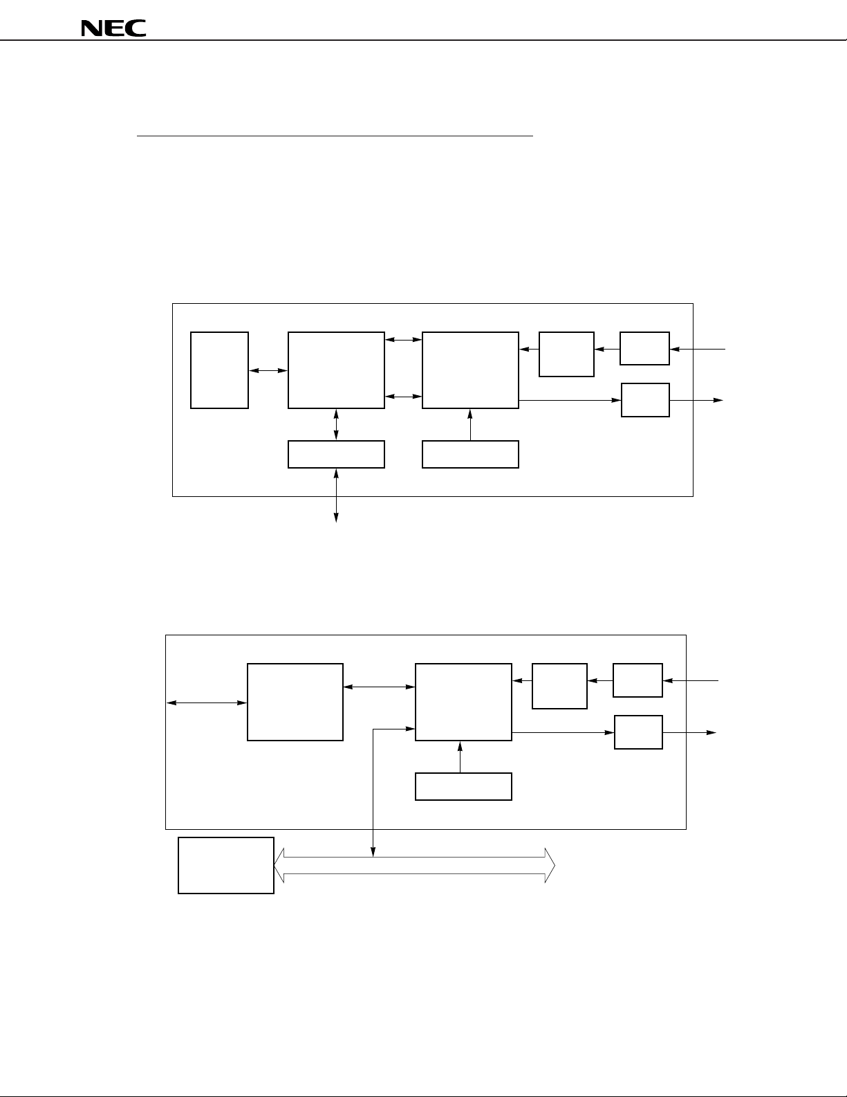
APPLICATION EXAMPLES
The followings are examples of the terminal equipment and the ATM Hub application using the µPD98402A.
NIC APPLICATION
DATA I/F (UTOPIA)
CONTROL
MEMORY
PD98401A
m
SAR CHIP
CNT I/F
PD98402A
m
PHY CHIP
155.52MHz
CLOCK
RECOVERY
CHIP
Rx PMD
TO HUB
Tx PMD
HOST BUS I/F
SWITCH
SYSTEM
SYNTHESIZER
HOST BUS
HUB APPLICATION (NIC SIDE)
DATA I/F
(UTOPIA)
CNT I/F
PD98402A
m
PHY CHIP
SYNTHESIZER
155.52MHz
CLOCK
RECOVERY
CHIP
Rx PMD
TO NIC
Tx PMD
CONTROLLER BUSCONTROLLER
3
Page 4
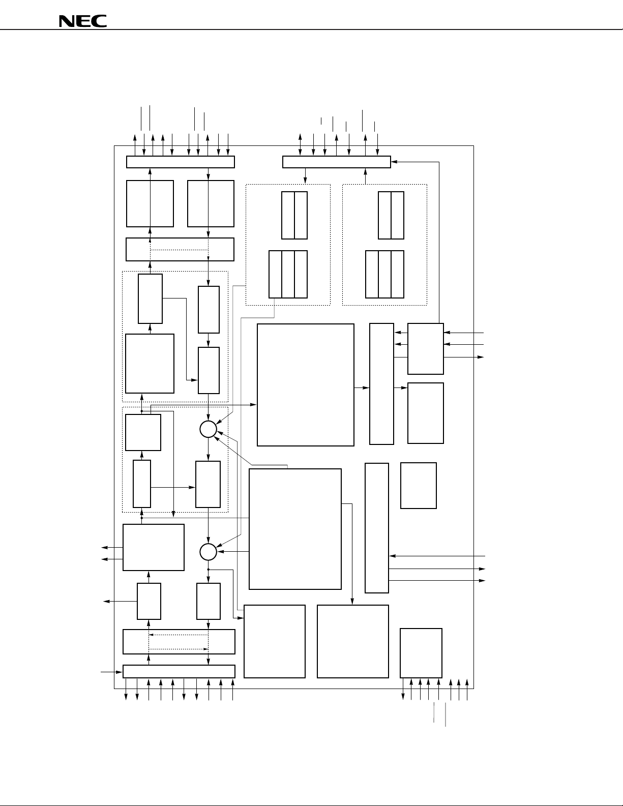
BLOCK DIAGRAM
RDO0—RDO7
RENBL
EMPTY
RSOC
RCLK
TDI0—TDI7
TENBL
FULL
TSOC
TCLK
D0—D7
A0—A5
R/W
ACK
CEOEPHINT
µ
PD98402A
ATM Layer Interface
Rx FIFO
4 Cell
Idle Cell
Drop
Loop Back
Cell
Descrambler
Cell Delineation
HEC Verification
HEC Correction
Generator
Rx Timing
Tx FIFO
4 Cell
HEC
Generator
Cell
Scrambler
+
Idle Cell
Insert
Management Interface
F2
C2
F1
Tx Overhead Registers
K2
C1(#1~#3)
Rx Overhead
Controller
F2
C2
F1
Rx Overhead Registers
K2
C1(#1~#3)
INT Cause
Registers
OAM Sequencer
Performance
Registers
RAL
TAL
LOS
Mode
Register
TFSS
TCL
TxFP
RxFP
OOF
RCL
Descrambler
A1, A2
SONET
Framing
Parallel
Serialfi
Scrambler
+
Parallel
fiSerial
Tx Overhead
Controller
Tx Timing Generator
Loop Back
BIP
Generator
PSEL
PMD Interface
RDIC, RDIT
TFKC, TFKT
TCOC, TCOT
TDOC, TDOT
TPC
TPD0-TPD7
RCIC, RCIT
TFC
RPC
RPD0-RPD7
(Tx)
BIP
Generator
(Rx)
TDO
Test
TJI
Block
TCK
TMS
TRST
DD
V
RESET
GND
4
Page 5
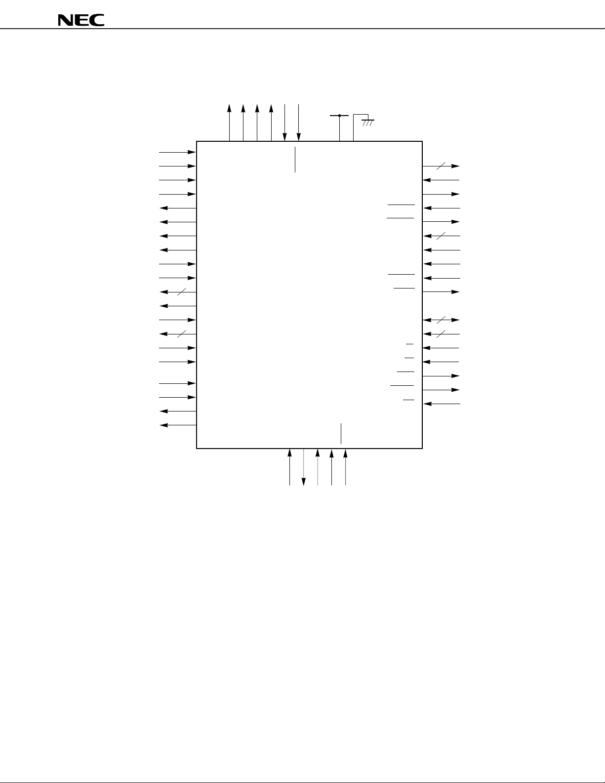
FUNCTIONAL PIN GROUPS
Control
µ
PD98402A
PMD
Interface
OAM
Interface
8
8
RDIC
RDIT
RCIC
RCIT
TDOC
TDOT
TCOC
TCOT
TFKC
TFKT
TPD0-TPD7
TPC
TFC
RPD0-RPD7
RPC
PSEL
RAL
TAL
LOS
OOF
RCL
TCL
TxFP
RxFP
TFSS
TJI
RESET
TDO
TCK
TMS
DD
V
TRST
GND
RDO0-RDO7
TDI0-TDI7
RCLK
RSOC
RENBL
EMPTY
TCLK
TSOC
TENBL
FULL
D0-D7
A0-A5
R/W
CE
ACK
PHINT
OE
8
ATM Layer
8
8
6
Interface
Management
Interface
Note
JTAG boundary scan
pin
Note This function can be supported at the customer’s request.
5
Page 6
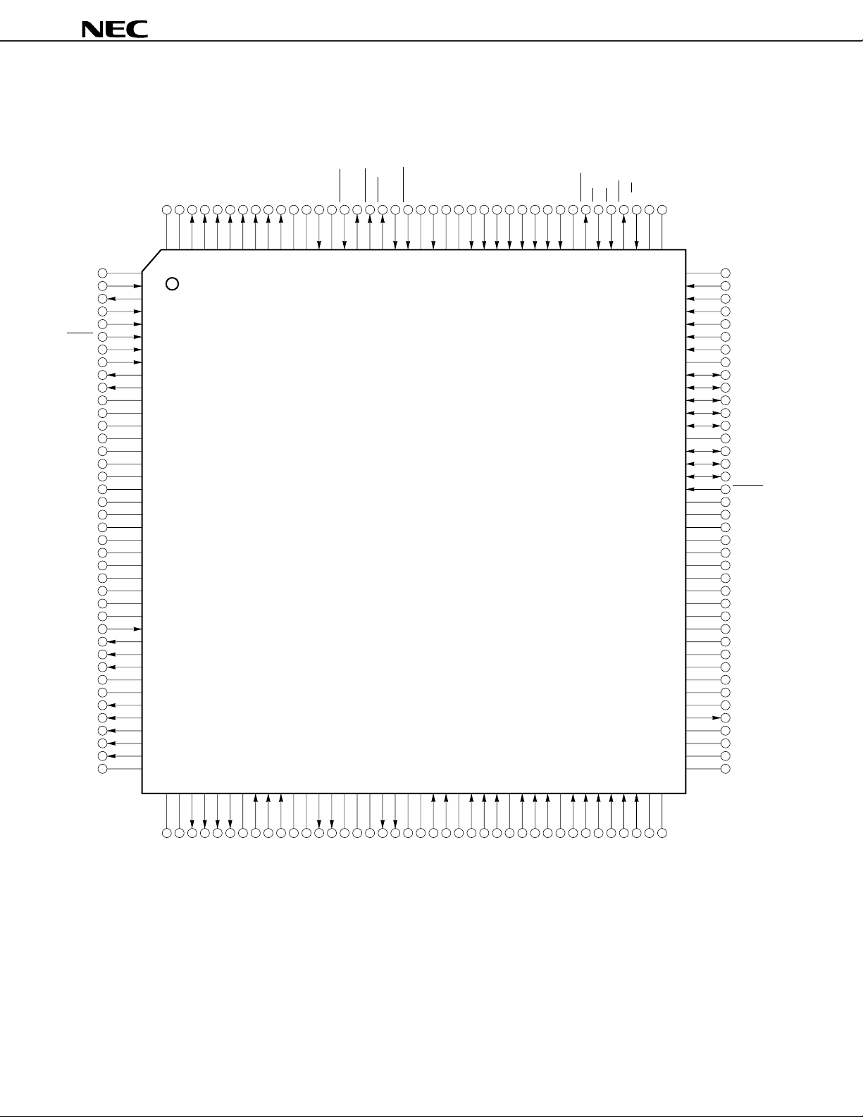
PIN CONFIGURATION
160-pin plastic QFP (FINE PITCH) (24 × 24 mm) (Top View)
µ
PD98402A
V
TCK
TDO
TJI
TMS
TRST
RAL
TAL
LOS
OOF
IC
IC
IC
IC
IC
IC
IC
IC
IC
V
GND
IC
IC
IC
IC
IC
IC
IC
TFSS
RxFP
TxFP
TCL
V
GND
TPD0
TPD1
TPD2
TPD3
TPD4
V
GND
GND
RDO7
RDO6
RDO5
RDO4
RDO3
RDO2
RDO1
DD
RDO0
V
GND
RCLK
GND
RENBL
RSOC
EMPTY
FULL
TSOC
TEMBL
GND
TCLK
GND
VDDTDI7
TDI6
TDI5
TDI4
TDI3
TDI2
TDI1
TDI0
GND
PHINTCEOE
ACK
R/W
GND
GND
121122123124125126127128129130131132133134135136137138139140141142143144145146147148149150151152153154155156157158159160
V
DD
1
2
3
4
5
6
7
8
9
10
11
12
13
14
15
16
µ
PD98402AGM-KED
17
18
19
DD
20
21
22
23
24
25
26
27
28
29
30
31
32
DD
33
34
35
36
37
38
39
DD
40
120
119
118
117
116
115
114
113
112
111
110
109
108
107
106
105
104
103
102
101
100
99
98
97
96
95
94
93
92
91
90
89
88
87
86
85
84
83
82
81
DD
A5
A4
A3
A2
A1
A0
GND
D7
D6
D5
D4
D3
GND
D2
D1
D0
RESET
CG
GND
DD
V
IC
IC
IC
IC
IC
GND
IC
IC
IC
IC
IC
IC
IC
IC
RCL
IC
IC
IC
DD
V
807978777675747372717069686766656462616059585756555453525150494847464544434241 63
GND
GND
TPD5
TPD6
TPC
TPD7
GND
TFC
TFKT
TFKC
GND
V
TCOT
TCOC
GND
V
DD
DD
DD
V
Remarks 1. IC : Internally Connected. Leave open.
2. CG : Connect to GND.
6
TDOT
TDOC
DD
V
GND
RCIT
RCIC
GND
RDIT
RPC
RDIC
GND
RPD7
RPD6
GND
RPD5
RPD4
RPD3
RPD2
RPD1
PSEL
RPD0
GND
GND
Page 7

A0-A5 : Address Bus
ACK : Read/write Cycle Receive Acknowledge
CE : Chip Enable
D0–D7 : Data Bus
EMPTY : Output Buffer Empty
FULL : Buffer Full
GND : Ground
LOS : Loss of Signal
OE : Output Enable
OOF : Out of Frame
PHINT : Physical Interrupt
PSEL : PMD I/F Select
RAL : Receive Alarm
RCIC : Receive Clock Input Complement
RCIT : Receive Clock Input True
RCL : Internal Receive System Clock
RCLK : Receive Data Transferring Clock from the ATM Layer Device
RDIC : Receive Data Input Complement
RDIT : Receive Data Input True
RDO0-RDO7 : Receive Data Output
RENBL : Receive Data Enable
RESET : System Reset
RPC : Receive Parallel Data Clock
RPD0-RPD7 : Receive Parallel Data
RSOC : Receive Start Address of ATM Cell
R/W : Read/write Control
RxFP : Receive Frame Pulse
TAL : Transmit Alarm
TCK : Test Clock
TCL : Internal Transmit System Clock
TCLK : Transmit Data Transferring Clock from the ATM Layer Device
TCOC : Transmit Clock Output Complement
TCOT : Transmit Clock Output True
TDI0-TDI7 : Transmit Data Input from the ATM Layer
TDO : Test Data Output
TDOC : Transmit Data Output Complement
TDOT : Transmit Data Output True
TENBL : Transmit Data Enable
TFC : Transmit Reference Clock
TFKC : Transmit Reference Clock Complement
TFKT : Transmit Reference Clock True
TFSS : Transmit Frame Set Signal
TJI : Test JTAG Data Input
TPC : Transmit Parallel Data Clock
TPD0-TPD7 : Transmit Parallel Data
TMS : Test Mode Select
TRST : Test Reset
TSOC : Transmit Start Address of ATM Cell
TxFP : Transmit Frame Pulse
DD : Supply Voltage
V
µ
PD98402A
7
Page 8
µ
PD98402A
1. PIN FUNCTIONS
• PMD Interface
Symbol Pin No. I/O I/O Level Function
RDIC 66 I Pseudo ECL These pins are used to input receive serial data when serial
Complement (–) interface mode is used (PSEL pin input = low level). Ground
RDIT 65 I Pseudo ECL
True (+)
RCIC 63 I Pseudo ECL These pins are used to input the receive system clock when
Complement (–) serial interface mode is used (PSEL pin input = low level).
RCIT 62 I Pseudo ECL
True (+)
TDOC 59 O Pseudo ECL These pins are used to output transmit serial data when serial
Complement (–) interface mode is used (PSEL pin input = low level). They are
TDOT 58 O Pseudo ECL
True (+)
TCOC 54 O Pseudo ECL These pins are used to output transmit clocks when serial
Complement (–) interface mode is used (PSEL pin input = low level). Transmit
TCOT 53 O Pseudo ECL
True (+)
TFKC 50 I Pseudo ECL These pins are used to input transmit system clocks when
Complement (–) serial interface mode is used (PSEL pin input = low level).
TFKT 49 I Pseudo ECL
True (+)
them when Parallel interface mode is used.
Clocks are input in synchronization with receive data. Ground
them when parallel interface mode is used.
open-drain pins. Terminate them with VDD –2 V via a 50 Ω
resistor. To be undefined after reset.
clocks to be input to the TFKC/TFKT pins are output passing
through internal gates. They are open-drain pins. Terminate
them with VDD –2 via a 50 Ω resistor. To be undefined after
reset.
Transmit data output from the TDOC/TDOT pins is output in
synchronization with clocks that are input to these pins.
Ground them when parallel interface mode is used.
RPD0-RPD7 77-73, 71-69 I TTL These pins are used to input receive parallel data when
parallel interface mode is used (PSEL pin input = high level).
Leave them open when serial interface mode is used.
RPC 67 I TTL This pin is used to input the receive system clock when
parallel interface mode is used (PSEL pin input = high level).
Input clocks synchronous with the receive data. Leave it open
when serial interface mode is used.
TPD0-TPD7 35-39, 43-45 O CMOS These pins are used to output transmit parallel data when
parallel interface mode is used (PSEL pin input = high level).
Leave them open when serial interface mode is used.
TPC 46 O CMOS This pin is used to output transmit clocks when parallel
interface mode is used (PSEL pin input = high level). Transmit
clocks to be input to the TFC pin are output passing through
internal gates. Leave it open when serial interface mode is
used.
TFC 48 I TTL This pins is used to input transmit system clocks when parallel
interface mode is used (PSEL pin input = high level). Transmit
data output from pins TPD0 to TPD7 are output in
synchronization with the clocks input to this pin. Leave it open
when serial interface mode is used.
PSEL 78 I CMOS This pin is used to select the mode for PMD interface serial/
parallel interface.
Low level: Serial interface mode
High level: Parallel interface mode
8
Page 9

µ
PD98402A
• Power supply
Symbol Pin No. I/O Function
VDD 1, 20, 33, 40, – Supply voltage, 5 V ±5 %
52, 55, 57, 60,
81, 100, 120,
137, 150
GND 21, 34, 41, 42, – Ground
47, 51, 56, 61,
64, 68, 72, 79,
80, 94, 101,
107, 113, 121,
122, 128, 138,
140, 147, 149,
159, 160
• ATM Layer Interface
Symbol Pin No. I/O I/O Level Function
RDO0-RDO7 151-158 O CMOS Connected to 8-bit data bus to output the receive data to the
ATM Layer device. Output is synchronized with the RCLK
rising up. To be undefined after reset.
RCLK 148 I TTL Input pin of the receive data transferring clock from the ATM
Layer device.
RSOC 145 O CMOS Receive cell start address signal. To the ATM Layer device,
this signal indicates the start address byte of the receive ATM
cell. To be undefined after reset.
RENBL 146 I TTL Receive enable signal. Input pin of the signal indicating that
the ATM layer device can receive data.
EMPTY 144 O CMOS Output buffer empty signal. This signal indicates that there is
no data to be transferred to the receive FIFO of the
µ
PD98402A. To be inactive after reset.
TDI0-TDI7 129-136 I TTL 8-bit data bus to input the transmit data from the ATM Layer
device. Reading a data on the bus is synchronized with the
TCLK rising-up.
TCLK 139 I TTL Input pin of the transmit data transferring clock from the ATM
layer device.
TSOC 142 I TTL Transmit cell start address signal. Input pin of the signal
indicating the start byte of the transmit ATM cell input from the
ATM Layer device to the µPD98402A.
TENBL 141 I TTL Transmit enable signal. This signal indicates that the ATM
Layer device is transmitting the valid data to the TDI0-TDI7.
FULL 143 O CMOS Input buffer full signal. When 4 bytes remain as the
acceptable bytes of transmit FIFO at last, this signal changes
to active. To be inactive after reset.
9
Page 10

µ
PD98402A
• Management Interface
Symbol Pin No. I/O I/O Level Function
D0-D7 104-106 I/O CMOS 8-bit data bus for data transfer between the control processor
108-112 and the internal register of the µPD98402A.
A0-A5 114-119 I TTL Address bus. Used for setting the internal register address of
the µPD98402A.
R/W 123 I TTL Read/write control signal.
Low level: Write cycle
High level: Read cycle
CE 126 I TTL Chip enable signal.
At low level, internal register access is to be enable.
ACK 124 O CMOS Read/write cycle receive acknowledge or ready signal.
After reset, this signal indicates inactive level.
PHINT 127 O CMOS Signal which indicates the interrupt cause occurrence to the
processor.
After reset, this signal indicates inactive level.
OE 125 I TTL Output enable. When this signal is set to low level, the
µ
PD98402A outputs data to the control bus. Even if the CE
signal is inactive, when this signal is at low level, the
µ
PD98402A drives the control bus.
• OAM Interface
Symbol Pin No. I/O I/O Level Function
LOS 9 O CMOS Loss of signal detection. Output high level when receive serial
data input is "0" for 50 µs continuously or optical input stop
signal (RAL) is input. When 2 consecutive frames of valid
synchronous pattern is detected, or when input of the optical
input stop signal is released, low level is output. To be
inactive after reset.
OOF 10 O CMOS Out of frame detection. When 4 consecutive frames of wrong
synchronous pattern are detected, high level is output. When
2 consecutive frames of normal synchronous pattern are
detected, low level is output. To be inactive after reset.
RAL 7 I TTL Receive alarm. Inputs receiver-side optical input stop signal
by the optical module.
Low level: Normal
High level: Optical input stopped.
TAL 8 I TTL Transmit alarm. Inputs transmit-side optical output stop signal
output by the optical module.
Low level: Normal
High level: Optical output stopped.
10
Page 11

µ
PD98402A
• Control
Symbol Pin No. I/O I/O Level Function
TFSS 29 I TTL This is the transmit frame setting signal input pin.
It allows synchronization timing of transmit frame output to be
set. The µPD98402A samples this input signal by the internal
transmit system clock (TCL).
Initial output of the transmit frame is restarted 9 clocks into
TCL clock cycle after a high level is latched at TCL rise.
RESET 103 I TTL This is the system reset signal input pin.
It initializes the µPD98402A. It is necessary to input a reset
signal with a pulse width of 2 cycles or more of the clock that
has the longest cycle among the following clocks input to the
µ
PD98402A.
ATM layer : TCLK, RCLK clock cycles
PMD layer : 1/8 cycle of TFKT/TFKC, RCIC/RCIT clocks,
TFC, RPC clock cycles
Immediately after a reset, no read/write is possible to registers
during 5 clocks of the TCL clock (19.44 MHz).
TCL 32 O CMOS This pin is used to output an internal transmit system clock.
The µPD98402A outputs as the internal transmit system clock,
the TFKT/TFKC input clock (155.52 MHz) scaled by 8 in serial
interface mode, and the TFC input clock (19.44 MHz) in
parallel interface mode.
RCL 85 O CMOS This pin is used to output an internal receive system clock.
The µPD98402A outputs as the internal receive system clock,
the RCIC/RCIT input clock (155.52 MHz) scaled by 8 in serial
interface mode, and the RFC input clock (19.44 MHz) in
parallel interface mode.
TxFP 31 O CMOS This is a frame pulse signal on the transmitting side. It
outputs pulses synchronous with the transmit frame start. To
be inactive after reset.
RxFP 30 O CMOS This is a frame pulse signal on the receiving side. It outputs
pulses synchronous with the receive frame start. To be
inactive after reset.
• JTAG boundary scan pins (This function can be supported at the customer’s request.)
Symbol Pin No. I/O I/O Level Function
TJI 4 I TTL This is a pin for JTAG boundary scan.
Pull it up or ground it in normal operation.
TDO 3 O CMOS This is a pin for JTAG boundary scan.
Leave it open in normal operation.
TCK 2 I TTL This is a pin for JTAG boundary scan.
Pull it up or ground it in normal operation.
TMS 5 I TTL This is a pin for JTAG boundary scan.
Pull it up or ground it in normal operation.
TRST 6 I TTL This is a pin for JTAG boundary scan.
Ground it in normal operation.
11
Page 12

• Recommended Connection for Unused Pins
Pin Recommended connection
TDOC, TDOT, TCOC, TCOT, ACK, LOS,
OOF, TCL, TxFP, RxFP
RAL, TAL, TFSS connect to GND
leave open
µ
PD98402A
12
Page 13

µ
PD98402A
2. ELECTRICAL SPECIFICATION
Absolute maximum ratings
Parameters Symbol Conditions Ratings Unit
Supply voltage VDD –0.5 to +6.5 V
Input/output voltage VI/VO –0.5 to VDD +0.5 V
Operating ambient temperature TA 0 to +70 °C
Storage temperature Tstg –65 to +150 °C
Caution Exposure to absolute maximum ratings for extended periods may affect device reliability;
exceeding the ratings could cause permanent damage. The parameters apply independently.
The device should be operated within the limits specified under DC and AC characteristics.
Capacitance
Parameters Symbol Conditions MIN. TYP. MAX. Unit
Input capacitance CI 10 20 pF
Output capacitance CO f = 1 MHz 10 20 pF
Input/output capacitance CIO 10 20 pF
Recommended operating conditions
Parameters Symbol Conditions MIN. TYP. MAX. Unit
Supply voltage VDD 4.75 5.25 V
Operating ambient temperature TA 0 +70 °C
VIL1 Note1 0 +0.8
Low level input voltage VIL2 Note2 VDD–2 VDD–1.5 V
VIL3 Note3 0 0.3 VDD
VIH1 Note1 2.2 VDD
High level input voltage VIH2 Note2 VDD–1.1 VDD V
VIH3 Note3 0.7 VDD VDD
Notes 1. TTL input pin
2. Pseudo ECL input pin
3. CMOS input pin
13
Page 14

µ
PD98402A
DC Characteristics (VDD = 5 V ±0.25 V, TA = 0 to +70 °C)
Parameters Symbol Conditions MIN. TYP. MAX. Unit
Note4
Note4
Note1
Note2
—10
—10
0.7 VDD —
— 0.4
Off-state output current IOZ VI = VDD or GND
ILI1 VI = VDD or GND
Input leak current
ILI2 Note 3 —10
VOH1 IOH = –0.5 mA
High level output voltage V
VOH2 Note 5 VDD–0.9 VDD–0.4
VOL1 IOL = 6.0 mA
Low level output voltage V
VOL2 Note 5 VDD–2.0 VDD–1.7
Supply current IDD Normal operation — 300 mA
Notes 1. 3-state data bus
2. TTL input pin
3. Pseudo ECL input pin
4. CMOS output pin
5. Pseudo ECL output pin
µ
A
µ
A
14
Page 15

µ
PD98402A
AC Characteristics
(1) Management Interface
Internal Register Read/Write
Parameters Symbol Conditions MIN. TYP. MAX. Unit
A0-A5 setup time (to CE↓)tSCC1 5
R/W setup time (to CE↓)tSCC2 5
A0-A5 hold time (to CE↓)tHCC1 3
R/W hold time (to CE↓)tHCC2 3
CE↓→ACK↓ delay time (read) tDCNAR Load capacitor 15 pF 3 × 4.5 ×
At parallel data input tCYPPR tCYPPR
Load capacitor 15 pF 3 × 4.5 ×
At serial data input (tCYPSR × 8) (tCYPSR × 8)
CE↓→ACK↓ delay time (write) tDCNAW Load capacitor 15 pF 2 × 3.5 ×
At parallel data input tCYPPR tCYPPR
Load capacitor 15 pF 2 × 3.5 ×
At serial data input (tCYPSR × 8) (tCYPSR × 8)
CE↑→ACK↑ delay time tDCPA Load capacitor 15 pF 1 × 2.5 ×
At parallel data input tCYPPR tCYPPR
Load capacitor 15 pF 1 × 2.5 ×
At serial data input (tCYPSR × 8) (tCYPSR × 8)
CE↓→ data output delay time tDCD Load capacitor 15 pF 2 × 3.5 ×
At parallel data input tCYPPR tCYPPR
Load capacitor 15 pF 2 × 3.5 ×
At serial data input (tCYPSR × 8) (tCYPSR × 8)
OE↓→ data output delay time tDOD Load capacitor 15 pF — 9.4 ns
OE↑→ data floating output delay time tFOD Load capacitor 15 pF — 10 ns
D0-D7 setup time (to CE↓)tSDC 5—ns
D0-D7 hold time (to CE↓)tHCD 3—ns
CE low-level width tCEBW At parallel data input 3.5 × —
tCYPPR
At serial data input 3.5 × —
(tCYPSR × 8)
OE low-level width tOEBW At parallel data input 2.5 × —
tCYPPR
At serial data input 2.5 × —
(tCYPSR × 8)
ns
ns
ns
ns
ns
ns
ns
ns
Remarks 1. For tCYPPR, refer to (6) PMD parallel interface timing.
2. For t
CYPSR, refer to (7) PMD serial interface timing.
15
Page 16

Management Interface
Internal Register Read
(a) Case 1 When the host uses ACK signal
t
SCC1
A0-A5
t
HCC1
µ
PD98402A
R/W
SCC2
t
t
CEBW
t
HCC2
CE
t
OEBW
OE
t
DCNAR
ACK
D0-D7
t
DOD
t
Valid
DCD
(b) Case 2 When the host does not use ACK signal
t
A0-A5
R/W
CE
SCC1
t
SCC2
t
HCC1
t
HCC2
t
t
CEBW
DCPA
t
FOD
16
OE
D0-D7
t
DOD
t
OEBW
Valid
t
FOD
Page 17

Internal Register Write
A0-A5
R/W
CE
t
t
SCC1
SCC2
t
HCC1
t
HCC2
t
DCPA
µ
PD98402A
ACK
D0-D7
OE
t
SDC
t
DCNAW
Valid
t
HCD
“ H ”
(2) OAM Interface
Parameters Symbol Conditions MIN. TYP. MAX. Unit
TCL↑→LOS delay time tDCLS load capacitor = 15 pF 5 30 ns
RCL↑→OOF delay time tDCOF load capacitor = 15 pF –5 +7 ns
OAM Interface
TCL
RCL
t
DCLS
LOS
OOF
DCOF
t
17
Page 18

µ
PD98402A
(3) Control Signal Interface
Parameters Symbol Conditions MIN. TYP. MAX. Unit
TCL↑→TPC delay time tDTCP load capacitor = 15 pF 0 +5 ns
TFSS setup time (to TCL↑)tSFSC 10 — ns
TFSS hold time (to TCL↑)tHCFS 5—ns
TCL↑→TxFP delay time tDCFP load capacitor = 15 pF 0 +20 ns
RCL↑→RxFP delay time t DCRP load capacitor = 15 pF –5 +20 ns
Control Signal Interface
TPC
t
DTCP
TCL
t
TFSS
DCFP
t
DCFP
TxFP
RCL
RxFP
t
SFSC
t
HCFS
t
DCRP
t
DCRP
18
Page 19

µ
PD98402A
(4) SAR Interface (Transmitter Side)
Parameters Symbol Conditions MIN. TYP. MAX. Unit
TCLK cycle time tCYST 30 125 ns
TCLK high level width tSTH 12 110 ns
TCLK low level width tSTL 12 110 ns
TCLK↑→FULL↓ delay time tFD load capacitor = 15 pF 5 17 ns
TDI0-TDI7 setup time (to TCLK↑)tSTDK1 5—ns
TSOC setup time (to TCLK↑)tSTDK2 12 — ns
TENBL setup time (to TCLK↑)tSTDK3 5—ns
TDI0-TDI7 hold time (to TCLK↑)tHKTD1 3—ns
TSOC hold time (to TCLK↑)tHKTD2 3—ns
TENBL hold time (to TCLK↑)tHKTD2 3—ns
SAR Interface (Transmitter Side)
TCLK
FULL
TENBL
TSOC
TDI0-TDI7
CYST
t
t
STHtSTL
t
t
t
FD
t
STDK2
HKTD3
t
HKTD2
STDK3
t
STDK1
P48 H1 Invalid H2 H3
t
HKTD1
19
Page 20

µ
PD98402A
(5) SAR Interface (Receiver Side)
Parameters Symbol Conditions MIN. TYP. MAX. Unit
RCLK cycle time tSYCR 30 125 ns
RCLK high level width tSRH 12 110 ns
RCLK low level width tSRL 12 110 ns
RCLK↑→EMPTY↑↓delay time tED load capacitor = 15 pF 5 17 ns
RENBL setup time (to RCLK↑)tSREK 12 — ns
RENBL hold time (to RCLK↑)tHKRE 3—ns
RCLK↑→RSOC↑↓ delay time tRSD load capacitor = 15 pF 0 17 ns
RCLK↑→RDO0-RDO7 delay time tRDD load capacitor = 15 pF 0 17 ns
SAR Interface (Receiver Side)
t
SYCR
RCLK
EMPTY
RENBL
RSOC
RDO0-RDO7
t
SRHtSRL
t
SREK
t
t
RSD
RDD
t
ED
t
ED
t
RSD
t
RDD
P48 H1 H2 H3
t
HKRE
20
Page 21

µ
PD98402A
(6) PMD Parallel Interface
Parameters Symbol Conditions MIN. TYP. MAX. Unit
RPC cycle time tCYPPR 50 — ns
RPC high level width tPPRH 20 — ns
RPC low level width tPPRL 20 — ns
TFC cycle time tCYPPT 50 — ns
TFC high level width tPPTH 20 — ns
TFC low level width tPPTL 20 — ns
RPD0-RPD7 setup time (to RPC↑)tSPDC 5—ns
RPD0-RPD7 hold time (to RPC↑)tHPCD 3—ns
TFC↑→TPC↑ delay time tDFPCP load capacitor = 15 pF 3 25 ns
TFC↓→TPC↓ delay time tDFPCN load capacitor = 15 pF 3 25 ns
TPC↑→TPD0-TPD7 delay time tDPCD load capacitor = 15 pF –3.0 +1.0 ns
PMD Parallel Interface
Receive Side
RPD0-RPD7
Transmit Side
TPD0-TPD7
RPC
TFC
TPC
t
PPRH
t
DFPCPtDFPCN
t
CYPPR
t
PPRL
SPDC
t
t
PPTH
t
HPCD
t
CYPPT
t
PPTL
DPCD
t
21
Page 22

µ
PD98402A
(7) PMD Serial Interface
Parameters Symbol Conditions MIN. TYP. MAX. Unit
RCIT (RCIC) cycle time tCYPSR 6.4 — ns
TFKT (TFKC) cycle time tCYPST 6.4 — ns
Serial data setup time tSSDC 1.0 — ns
Serial data hold time tHSCD 1.0 — ns
Serial clock delay time (rising) tDFSCP Load capacitor 15 pF — 8 ns
Serial clock delay time (falling) tDFSCN Load capacitor 15 pF — 8 ns
Transmit serial data delay time tDSCD Load capacitor 15 pF — 3 ns
PMD Serial Interface
Receive Side
t
CYPSR
Transmit Side
RCIC, RCIT
RDIC, RDIT
TFKC, TFKT
TCOC, TCOT
TDOC, TDOT
t
DFSCPtDFSCN
t
DSCD
t
SSDC
t
HSCD
t
CYPST
22
Page 23

3. PACKAGE DRAWING
160 PIN PLASTIC QFP (FINE PITCH) ( 24)
A
B
120 81
121
80
µ
PD98402A
detail of lead end
160
1
41
40
F
G H IJ
M
P
N
NOTE
Each lead centerline is located within 0.10 mm (0.004 inch) of
its true position (T.P.) at maximum material condition.
C D
S
Q
K
M
L
ITEM MILLIMETERS INCHES
A 26.0±0.2 1.024
B
24.0±0.2
C 24.0±0.2
D 26.0±0.2 1.024
F
2.25
G 2.25
H 0.22 0.009±0.002
I 0.10 0.004
J 0.5 (T.P.) 0.020 (T.P.)
K 1.0±0.2 0.039
L 0.5±0.2 0.020
M 0.17 0.007
N 0.10 0.004
P 2.7 0.106
Q 0.125±0.075
R 5°±5° 5°±5°
S 3.0 MAX. 0.119 MAX.
R
+0.008
–0.009
0.945±0.008
0.945±0.008
+0.008
–0.009
0.089
0.089
+0.05
–0.04
+0.009
–0.008
+0.008
–0.009
+0.03
–0.07
S160GM-50-3ED, JED, KED-2
+0.001
–0.003
0.005±0.003
23
Page 24

µ
PD98402A
4. RECOMMENDED SOLDERING CONDITIONS
For the µPD98402A, soldering must be performed under the following conditions.
For details of recommended conditions for surface mounting, refer to information document “Semiconductor
Device Mounting Technology Manual” (IEI-1207).
For other soldering methods, please consult with NEC sales personnel.
µ
PD98402AGM-KED: 160-pin plastic QFP (FINE PITCH) (24 × 24 mm)
•
Soldering Method Soldering Conditions Symbol
Package peak temperature: 235 °C, time: 30 sec. max. (over 210 °C), count:
twice or less, restriction days: 3
is necessary)
Infrared reflow Precautions: IR35-203-2
(1) Reflow a second time should be started when the device temperature has
returned to its normal state after the first reflow.
(2) Avoid flux cleaning with water after the first reflow.
Pin partial heating Pin temperature: 300 °C max., time: 3 seconds max. (per side) —
Note This means the number of days after unpacking the dry pack. Storage conditions are 25 °C and 65 % RM
max.
Note
(after that, 125 °C pre-baking for 20 hours
24
Page 25

[MEMO]
µ
PD98402A
25
Page 26

µ
PD98402A
[MEMO]
The export of this product from Japan is prohibited without governmental license. To export or re-export this product from
a country other than Japan may also be prohibited without a license from that country. Please call an NEC sales
representative.
No part of this document may be copied or reproduced in any form or by any means without the prior written
consent of NEC Corporation. NEC Corporation assumes no responsibility for any errors which may appear in this
document.
NEC Corporation does not assume any liability for infringement of patents, copyrights or other intellectual
property rights of third parties by or arising from use of a device described herein or any other liability arising
from use of such device. No license, either express, implied or otherwise, is granted under any patents,
copyrights or other intellectual property rights of NEC Corporation or others.
While NEC Corporation has been making continuous effort to enhance the reliability of its semiconductor devices,
the possibility of defects cannot be eliminated entirely. To minimize risks of damage or injury to persons or
property arising from a defect in an NEC semiconductor device, customer must incorporate sufficient safety
measures in its design, such as redundancy, fire-containment, and anti-failure features.
NEC devices are classified into the following three quality grades:
“Standard“, “Special“, and “Specific“. The Specific quality grade applies only to devices developed based on
a customer designated “quality assurance program“ for a specific application. The recommended applications
of a device depend on its quality grade, as indicated below. Customers must check the quality grade of each
device before using it in a particular application.
Standard:Computers, office equipment, communications equipment, test and measurement equipment,
audio and visual equipment, home electronic appliances, machine tools, personal electronic
equipment and industrial robots
Special: Transportation equipment (automobiles, trains, ships, etc.), traffic control systems, anti-disaster
systems, anti-crime systems, safety equipment and medical equipment (not specifically designed
for life support)
Specific: Aircrafts, aerospace equipment, submersible repeaters, nuclear reactor control systems, life
support systems or medical equipment for life support, etc.
The quality grade of NEC devices in “Standard“ unless otherwise specified in NEC's Data Sheets or Data Books.
If customers intend to use NEC devices for applications other than those specified for Standard quality grade,
they should contact NEC Sales Representative in advance.
Anti-radioactive design is not implemented in this product.
26
M4 94.11
 Loading...