

Page 1

DATA SHEET
MOS INTEGRATED CIRCUIT
m
PD78P368A
16/8 BIT SINGLE-CHIP MICROCOMPUTER
The mPD78P368A is produced by replacing the internal mask ROM of the mPD78366A with a one-time PROM
or EPROM. One-time PROM products, in which data can be written once are effective for manufacture of small
quantities of multiple products and early stage start-up of application. EPROM products, to which programs can
be re-written after previously written programs have been erased, are suited for system evaluation.
The following user's manual describes the details of functions. Be sure to read it before design.
m
PD78366A User's Manual, Hardware: U10205E
m
PD78356 User's Manual, Instructions: IEU-1395
FEATURES
• Compatible with the
• Can be replaced with the
• Internal PROM: 48K bytes
• Data can be written once (one-time PROM product without an erasure window)
• Written data can be erased by exposure to ultraviolet light and re-written electrically (EPROM product with an
erasure window)
• PROM programming characteristics: Compatible with the
• QTOP
ORDERING INFORMATION
TM
microcomputer
Remark The QTOP microcomputer is a single-chip microcomputer with a built-in one-time PROM that is totally
supported by NEC. The support includes writing application programs, marking, screening, and
verification.
Part number Package Internal ROM
m
PD78P368AGF-3B9 80-pin plastic QFP (14 ¥ 20 mm) One-time PROM
m
PD78P368AKL-S
Note Under development
m
PD78366A
Note
m
PD78366A containing mask ROM on a full-production basis.
m
PD27C1001A
80-pin ceramic WQFN EPROM
In this manual, the description of the PROM is for both a one-time PROM and EPROM.
(Previous No. IP-3680)
Date Published June 1996 P
Printed in Japan
The information in this document is subject to change without notice.
The mark H shows major revised points.Document No. U11373EJ1V0DS00 (1st edition)
1996
©
1990
Page 2
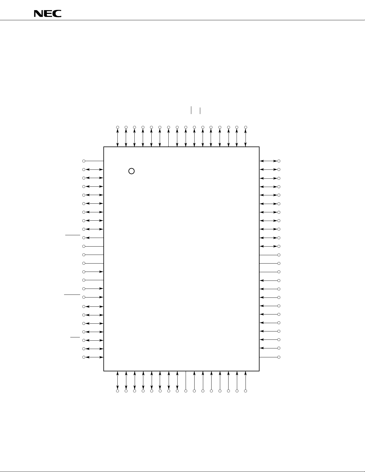
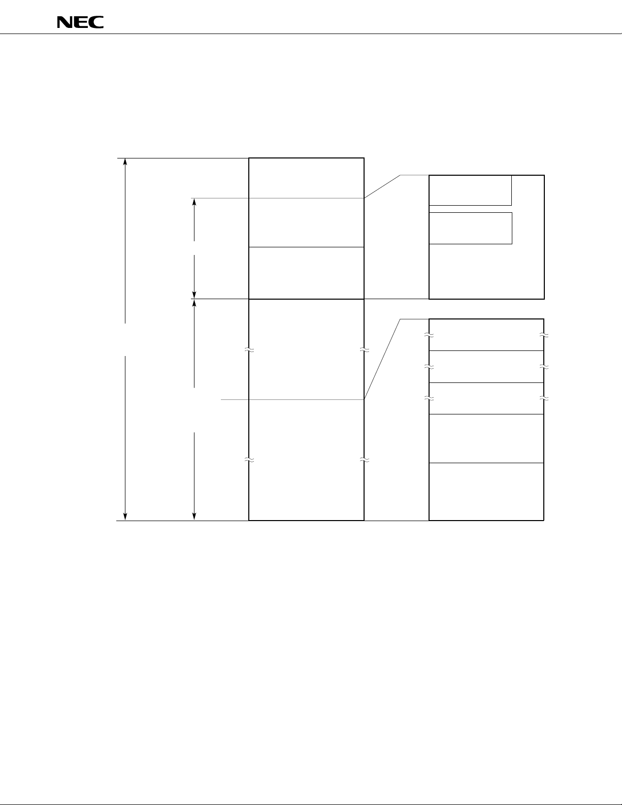
PIN CONFIGURATION (TOP VIEW)
(1) Normal operation mode (MODE0 = L, MODE1 = L)
• 80-pin plastic QFP (14 ¥ 20 mm)
m
PD78P368AGF-3B9
• 80-pin ceramic WQFN
m
PD78P368AKL-S
m
PD78P368A
V
P00/RTP0
P01/RTP1
P02/RTP2
P03/RTP3
P04/PWM0
P05/ TCUD/PWM1
P06/ TIUD/TO40
P07/ TCLRUD
WDTO
IC
V
V
X1
X2
MODE1
RESET
X
D0
P30/ T
P31/RXD0
P32/SO/SB0
P33/SI/SBI
P34/SCK
X
D1
P35/ T
X
D1
P36/R
P84/ TO04
P83/ TO03
P82/TO02
P81/ TO01
P80/ TO00
ASTB
P93
P92
P91/ WR
P90/RD
P57/A15
P56/A14
P55/A13
P54/A12
P53/A11
P85/ TO05
80 79 78 77 76 75 74 73 72 71 70 69 68 67 66 65
SS
DD
SS
1
2
3
4
5
6
7
8
9
10
11
12
13
14
15
16
17
18
19
20
21
22
23
24
64
63
62
61
60
59
58
57
56
55
54
53
52
51
50
49
48
47
46
45
44
43
42
41
P52/A10
P51/A9
P50/A8
P47/AD7
P46/AD6
P45/AD5
P44/AD4
P43/AD3
P42/AD2
P41/AD1
P40/AD0
SS
V
V
DD
AV
DD
AV
REF
P77/ANI7
P76/ANI6
P75/ANI5
P74/ANI4
P73/ANI3
P72/ANI2
P71/ANI1
P70/ANI0
SS
AV
25 26 27 28 29 30 31 32 33 34 35 36 37 38 39 40
P10
P11
P12
Caution Directly connect the IC pin to V
Remark Pin compatible with the mPD78366AGF
2
P13
SS.
P14
P15
P16
P17
SS
V
MODE0
P20/NMI
P21/INTP0
P22/INTP1
P23/INTP2
P25/INTP4
P24/INTP3/ TI
Page 3

m
PD78P368A
P00-P07: Port 0
P10-P17: Port 1
P20-P25: Port 2
P30-P36: Port 3
P40-P47: Port 4
P50-P57: Port 5
P70-P77: Port 7
P80-P85: Port 8
P90-P93: Port 9
RTP0-RTP3: Real-time port
NMI: Nonmaskable interrupt
INTP0-INTP4: Interrupt from peripherals
TO00-TO05, TO40: Timer output
TI: Timer input
TIUD: Timer input for up/down
counter
TCUD: Timer control for up/down
counter
TCLRUD: Timer clear for up/down
counter
ANI0-ANI7: Analog input
TxD0, TxD1: Transmit data
RxD0, RxD1: Receive data
SI: Serial input
SO: Serial output
SB0, SB1: Serial bus
SCK: Serial clock
PWM0, PWM1: Pulse width modulation output
WDTO: Watchdog timer output
MODE0, MODE1: Mode
AD0-AD7: Address/data bus
A8-A15: Address bus
ASTB: Address strobe
RD: Read strobe
WR: Write strobe
RESET: Reset
X1, X2: Crystal
DD: Analog VDD
AV
AVSS: Analog VSS
AVREF: Analog reference voltage
DD: Power supply
V
SS: Ground
V
IC: Internally connected
3
Page 4
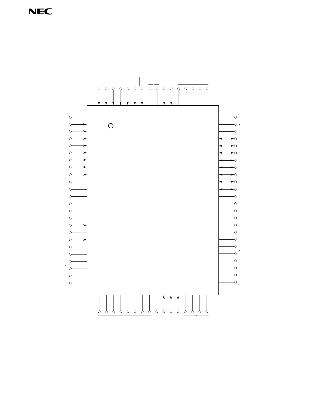
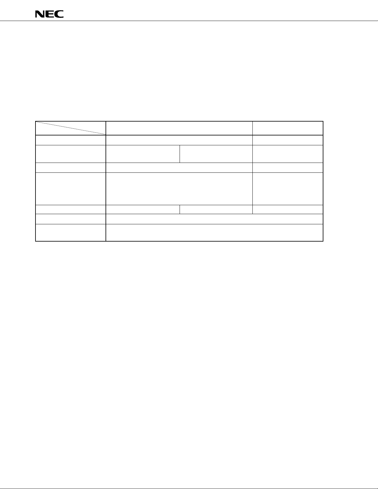
(2) PROM programming mode (MODE0/VPP = H, MODE1 = L)
• 80-pin plastic QFP (14 ¥ 20 mm)
m
PD78P368AGF-3B9
• 80-pin ceramic WQFN
m
PD78P368AKL-S
m
PD78P368A
VSS
A0
A1
A2
A3
A4
A5
A6
A7
(Open)
(G)
VDD
VSS
(G)
(Open)
MODE1
(G)
A16
(L)
(L)
A15
A14
A13
A11
A10
A12
80 79 78 77 76 75 74 73 72 71 70 69 68 67 66 65
1
2
3
4
5
6
7
8
9
10
11
12
13
14
15
16
17
18
19
20
21
22
23
24
25 26 27 28 29 30 31 32 33 34 35 36 37 38 39 40
PGM
CE
OE
(L)
64
63
62
61
60
59
58
57
56
55
54
53
52
51
50
49
48
47
46
45
44
43
42
41
D7
D6
D5
D4
D3
D2
D1
D0
V
VDD
VDD
(L)
SS
(G)
A9
VSS
(L)
A8
(G)
MODE0/ VPP
Caution Symbols in parentheses denote how the pins not used in the PROM programming mode should
be treated.
L: Connect these pins to the V
G: Connect these pins to the V
SS pins through separate resistors.
SS pins.
Open: Do not connect these pins to anything.
4
Page 5

m
PD78P368A
A0-A16: Address bus
D0-D7: Data bus
CE: Chip enable
OE: Output enable
PGM: Programming mode
MODE0, MODE1: Programming mode set
PP: Programming power supply
V
DD: Power supply
V
SS: Ground
V
5
Page 6
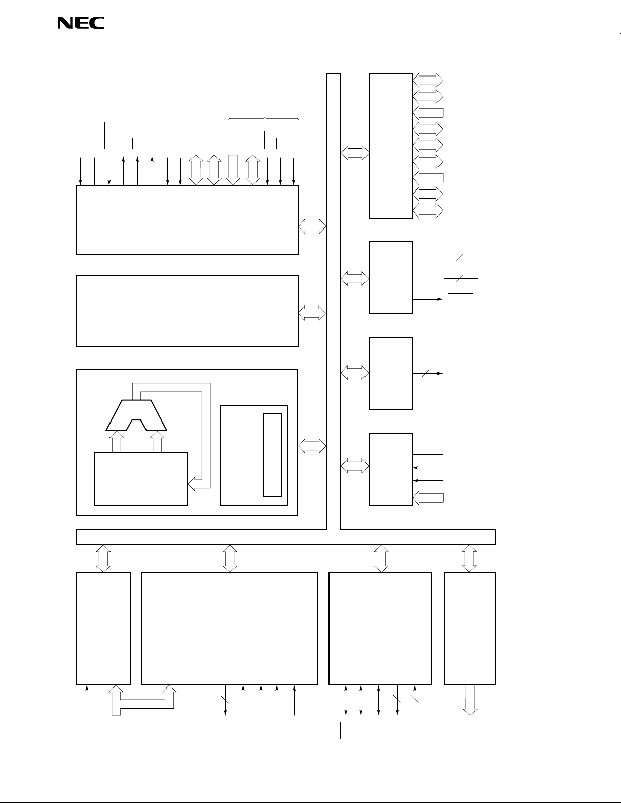
BLOCK DIAGRAM
X1X2RESET
BCU
ASTBRDWR
MODE1
System
control
Note
PP
MODE0/V
&
Bus
A8-A15
8
control
&
A0-A16
AD0-AD7
8
17
Prefetch
control
Note
D0-D7
8
PGM
CE
OE
Port
Watchdog
timer
m
PD78P368A
P0
8
8
P1
6
P2
7
P3
8
P4
P5
8
8
P7
6
P8
4
P9
2
DD
V
4
V
SS
WDTO
PROM/RAM
EXU
Main RAM
128 × 8
General
registers
ALU
&
PROM
Data
memory
Periph-
&
eral RAM
1792 × 8
Micro
sequence
control
Micro ROM
PWM
A/D
converter
2
PWM
DD
AV
AV
SS
AV
REF
INTP2
8
ANI
48K × 8
128 × 8
Note Shading indicates the pins used in the PROM programming mode.
(SBI)
(UART)
Serial
interface
Programmable
interrupt
NMI
controller
5
5
INTP
(Real-time pulse unit)
Timer/counter unit
4
7
TI
TO
TIUD
TCUD
TCLRUD
SCK
SO/SB0
2
SI/SB1
TxD
2
RxD
Real-time output
port
4
RTP
6
Page 7

m
PD78P368A
CONTENTS
1. PIN FUNCTIONS........................................................................................................................ 8
1.1 NORMAL OPERATION MODE (MODE0 = L, MODE1 = L) ......................................................... 8
1.2 PROM PROGRAMMING MODE (MODE0/V
1.3 INPUT/OUTPUT CIRCUIT TYPE FOR EACH PIN AND HANDLING OF UNUSED PINS .......... 1 1
PP = H, MODE1 = L) ................................................ 10
2. MEMORY CONFIGURATION................................................................................................... 13
3. DIFFERENCES BETWEEN THE mPD78P368A AND mPD78366A ......................................... 1 4
4. PROM PROGRAMMING ............................................................................................................ 15
4.1 OPERATION MODE........................................................................................................................ 15
4.2 PROCEDURE FOR WRITING ON PROM (PAGE PROGRAM MODE)............................... 16
4.3 PROCEDURE FOR WRITING ON PROM (BYTE PROGRAM MODE) ................................ 18
4.4 PROCEDURE FOR READING FROM PROM ........................................................................... 21
5. ERASURE CHARACTERISTICS (mPD78P368AKL-S ONLY) ................................................ 22
6. PROTECTIVE FILM COVERING THE ERASURE WINDOW (mPD78P368AKL-S ONLY)........ 22
7. SCREENING ONE-TIME PROM PRODUCTS.......................................................................... 22
8. ELECTRICAL SPECIFICATIONS ............................................................................................. 23
9. PACKAGE DRAWINGS ............................................................................................................. 39
10. RECOMMENDED SOLDERING CONDITIONS...................................................................... 41
APPENDIX A TOOLS...................................................................................................................... 42
A.1 DEVELOPMENT TOOLS ................................................................................................................ 42
A.2 EMBEDDED SOFTWARE............................................................................................................... 47
APPENDIX B DIMENSIONS OF THE CONVERSION SOCKET AND RECOMMENDED
PATTERN ON BOARDS ......................................................................................... 49
H
H
7
Page 8
1. PIN FUNCTIONS
1.1 NORMAL OPERATION MODE (MODE0 = L, MODE1 = L)
(1) Port pins
m
PD78P368A
P00-P03
P04
P05
P06
P07
P10-P17
P20
P21
P22
P23
P24
P25
P30
P31
P32
P33
P34
P35
P36
P40-P47
P50-P57
P70-P77
I/O Dual-function pinPin name
I/O
I/O
I/O
I/O
I/O
Function
Port 0.
8-bit I/O port.
Can be specified as input or output bit by bit.
Port 1.
8-bit I/O port.
Can be specified as input or output bit by bit.
I
I
Port 2.
Port used only for 6-bit input.
Port 3.
7-bit I/O port.
Can be specified as input or output bit by bit.
Port 4.
8-bit I/O port.
Can be specified as input or output in units of 8 bits.
Port 5.
8-bit I/O port.
Can be specified as input or output bit by bit.
Port 7.
Port used only for 8-bit input.
RTP0-RTP3
PWM0
TCUD/PWM1
TIUD/TO40
TCLRUD
–
NMI
INTP0
INTP1
INTP2
INTP3/TI
INTP4
TxD0
RxD0
SO/SB0
SI/SB1
SCK
TxD1
RxD1
AD0-AD7
A8-A15
ANI0-ANI7
8
P80-P85
P90
P91
P92
P93
I/O
I/O
Port 8.
6-bit I/O port.
Can be specified as input or output bit by bit.
Port 9.
4-bit I/O port.
Can be specified as input or output bit by bit.
TO00 - TO05
RD
WR
–
–
Page 9
(2) Non-port pins (1/2)
m
PD78P368A
RTP0-RTP3
NMI
INTP0
INTP1
INTP2
INTP3
INTP4
TI
TCUD
TIUD
TCLRUD
TO00-TO05
TO40
ANI0-ANI7
TxD0
TxD1
RxD0
RxD1
SCK
SI
SO
SB0
SB1
PWM0
PWM1
WDTO
AD0-AD7
A8-A15
ASTB
RD
WR
I/O
I/O
I/O
I/O
Function
O
I
I
O
I
O
I
I
O
O
O
O
Outputs a pulse in real time as triggered by a trigger signal sent from the
real-time pulse unit.
Nonmaskable interrupt request input
External interrupt request input
External count clock input to timer 1
Input for the control signal to determine whether the up/down counter (timer
4) counts up or down.
External count clock input to the up/down counter (timer 4)
Clear signal input to the up/down counter (timer 4)
Pulse output from the real-time pulse unit
Analog input to the A/D converter
Serial data output from the asynchronous serial interface
Serial data input to the asynchronous serial interface
Serial clock I/O for the clock synchronous serial interface
Serial data input to the clock synchronous serial interface in the 3-wire mode
Serial data output from the clock synchronous serial interface in the 3-wire
mode
Serial data I/O for the clock synchronous serial interface in the SBI mode
PWM signal output
Output for the signal which indicates the watchdog timer overflowed. (A
nonmaskable interrupt is generated.)
Multiplexed address/data bus used when external memory is expanded
Address bus used when external memory is expanded
Output for the timing signal used in externally latching address information
output from the AD0 to AD7 and A8 to A15 pins, in order to access the
external memory
Read strobe signal output to the external memory
Write strobe signal output to the external memory
Dual-function pinPin name
P00-P03
P20
P21
P22
P23
P24/TI
P25
P24/INTP3
P05/PWM1
P06/TO40
P07
P80-P85
P06/TIUD
P70-P77
P30
P35
P31
P36
P34
P33/SB1
P32/SB0
P32/SO
P33/SI
P04
P05/TCUD
–
P40-P47
P50-P57
–
P90
P91
9
Page 10
(2) Non-port pins (2/2)
m
PD78P368A
I/O Dual-function pinPin name
MODE0
MODE1
RESET
X1
X2
AVREF
AVDD
AVSS
VDD
VSS
IC
I
I
I
–
I
–
–
–
–
–
Input for the control signal which sets the operation mode. Normally, both
MODE0 and MODE1 are directly connected to the VSS pin.
System reset input
Crystal input pin for the system clock. A clock signal provided externally is
input to the X1 pin. The reversed signal of the clock signal is input to the
X2 pin.
A/D converter reference voltage input
Analog power supply for the A/D converter
Ground for the A/D converter
Positive power supply
Ground
Internally connected. Directly connect the IC pin to VSS.
1.2 PROM PROGRAMMING MODE (MODE0/V
Pin name
MODE0/VPP
MODE1
A0-A16
D0-D7
PGM
CE
OE
VDD
VSS
I/O
PROM programming mode set/programming supply voltage
I
PROM programming mode set
I
Address bus
I
Data bus
I/O
Program input
I
Enable PROM
I
Read strobe to PROM
I
Positive power supply
GND
Function
–
–
–
–
–
–
–
–
–
PP = H, MODE1 = L)
Function
10
Page 11
m
PD78P368A
1.3 INPUT/OUTPUT CIRCUIT TYPE FOR EACH PIN AND HANDLING OF UNUSED PINS
Table 1-1 lists the input and output circuit type for each pin and how to handle it when it is not used. Fig. 1-1 shows
the circuits.
Table 1-1 Input/Output Circuit Type for Each Pin and Recommended Connection Methods for Unused
Pins
P00/RTP0-P03/RTP3
P04/PWM0
P05/TCUD/PWM1
P06/TIUD/TO40
P07/TCLRUD
P10-P17
P20/NMI
P21/INTP0
P22/INTP1
P23/INTP2
P24/INTP3/TI
P25/INTP4
P30/TxD0
P31/RxD0
P32/SO/SB0
P33/SI/SB1
P34/SCK
P35/TxD1
P36/RxD1
P40/AD0-P47/AD7
P50/A8-P57/A15
P70/ANI0-P77/ANI7
P80/TO00-P85/TO05
P90/RD
P91/WR
P92, P93
ASTB
WDTO
MODE0, MODE1
RESET
AVREF, AVSS
AVDD
Pin
I/O circuit type
5-A
2
2-A
5-A
8-A
5-A
9
5-A
5
19
1
2
–
Recommended connection method
Input state: Each pin is connected to the V DD or
VSS pin via a separate resistor.
Output state: Open
Connected to the VSS pin.
Input state: Each pin is connected to the V DD or
VSS pin via a separate resistor.
Output state: Open
Connected to the VSS pin.
Input state: Each pin is connected to the V DD or
VSS pin via a separate resistor.
Output state: Open
Connected to the VSS pin.
–
Connected to the VSS pin.
Connected to the VDD pin.
11
Page 12
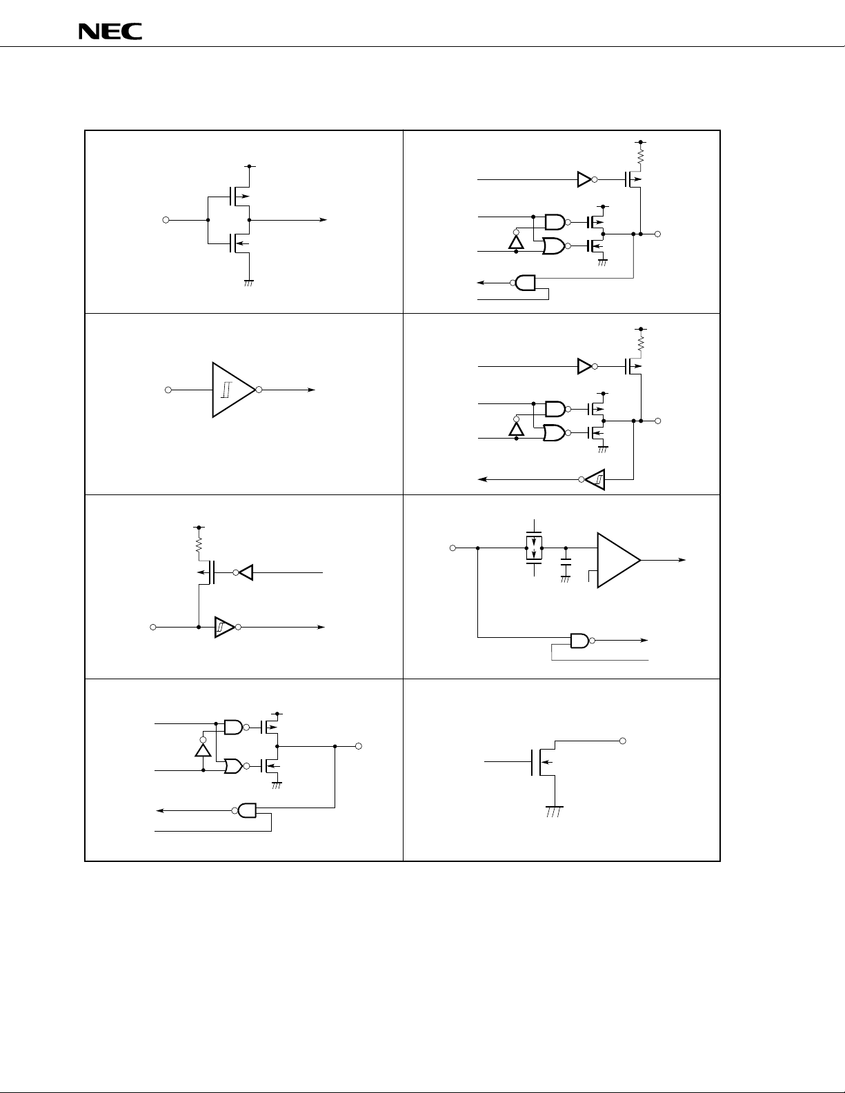
Fig. 1-1 Input/Output Circuits of Each Pin
Input
enable
Output
disable
Pull-up
enable
Data
IN/OUT
N-ch
V
DD
P-ch
V
DD
P-ch
N-ch
OUT
m
PD78P368A
Type 1 Type 5-A
DD
V
P-ch
IN
N-ch
Type 2 Type 8-A
Pull-up
IN
enable
Data
Output
disable
Schmitt trigger input with hysteresis characteristics
Type 2-A Type 9
V
DD
IN
P-ch
Pull-up
enable
IN
Schmitt trigger input with hysterisis characteristics
P-ch
N-ch
V
DD
P-ch
N-ch
Comparator
+
–
V
ref
(Threshold voltage)
V
DD
P-ch
Input
enable
IN/OUT
Type 5 Type 19
Data
Output
disable
V
DD
P-ch
IN/OUT
N-ch
Input
enable
12
Page 13
2. MEMORY CONFIGURATION
The mPD78P368A can access memory of up to 64K bytes. Fig. 2-1 shows the memory map.
Fig. 2-1 Memory Map
MODE 0, 1 = LL
Data memory
FFFFH
FF00H
FEFFH
FE00H
FDFFH
F700H
F6FFH
Special function
register (SFR)
(256 × 8)
Main RAM
(256 × 8)
Peripheral RAM
(1792 × 8)
FEFFH
FE80H
FE25H
FE06H
F700H
General register
(128 × 8)
Macro service control
(32 × 8)
m
PD78P368A
Data area
(2048 × 8)
Memory
space
(64K × 8)
Program
memory
Data
memory
C000H
BFFFH
0000H
External memory
(14080 × 8)
Internal PROM
(49152 × 8)
Note
BFFFH
1000H
0FFFH
0800H
07FFH
0080H
007FH
0040H
003FH
0000H
Program area
CALLF instruction
entry area
(2048 × 8)
Program area
CALLT instruction
table area
(64 × 8)
Vector table area
(64 × 8)
Note Access in the external memory expansion mode.
Caution When word access (including the stack operation) to the main RAM space (FE00H to FEFFH) is
executed, the addresses specified in the operand must be even numbers.
13
Page 14
m
PD78P368A
3. DIFFERENCES BETWEEN THE
mm
m
PD78P368A AND
mm
mm
m
PD78366A
mm
The mPD78P368A is produced by replacing the internal mask ROM of the mPD78366A with a 48K-byte PROM.
Both have the same functions except some differences in ROM specifications, such as write and verify modes. Table
3-1 shows the differences.
m
In this manual, the functions specific to the
m
to the
PD78366A document.
Table 3-1 Differences between the
Item
ROM
Internal program memory
(Electrical write)
PROM programming pin
Setting of MODE0 and
MODE1
Package
Electrical characteristics
Others
Part number
48K bytes
One-time PROM
(Data can be written once)
Provided
• Normal operation mode
MODE0, 1 = LL
• PROM programming mode
MODE0, 1 = HL
80-pin plastic QFP
They differ in supply current and other factors.
Since each product has a different circuit scale and mask layout, the noise immunity and
noise radiation of each product differ.
PD78P368A are explained. For details of the other functions, refer
mm
m
PD78P368A and mPD78366A
mm
m
m
PD78P368A
EPROM (Data can be
written multiple times)
80-pin ceramic WQFN
32K bytes
Mask ROM
Not provided
• Normal operation mode
• ROM-less mode
80-pin plastic QFP
PD78366A
MODE0, 1 = LL
MODE0, 1 = HH
Cautions1. The PROM and mask ROM products differ in noise immunity and noise radiation. Use not ES
products but CS products (mask ROM products) to evaluate them thoroughly when considering
the change from the PROM products to the mask ROM products during processes from
preproduction to volume production.
2. Connect the MODE0 and MODE1 pins directly to the V
DD or VSS pin.
14
Page 15
m
PD78P368A
4. PROM PROGRAMMING
The mPD78P368A is provided with an electrically writable PROM of 48K ¥ 8 bits. When programming this PROM,
use the MODE0/V
The
m
PD78P368A provides programming characteristics compatibility with the mPD27C1001A.
PP and MODE1 pins to set the
Table 4-1 Pin Functions in Programming Mode
m
PD78P368A to the PROM programming mode.
Function
Address input
Data input
Program pulse
Chip enable
Output enable
Program voltage
Mode control
Normal operation mode
P00-P07, P21, P20, P80-P85, P30
P40-P47
ASTB
P91
P90
MODE0/VPP
MODE1
Programming mode
A0-A16
D0-D7
PGM
CE
OE
4.1 OPERATION MODE
To enter the program write/verify mode, set each pin as follows: MODE0/V
PP = H, MODE1 = L. In addition, any
of the operation modes listed in Table 4-2 can be selected by setting the CE, OE, and PGM pins in this mode.
m
Set the
PD78P368A to the read mode in order to read the contents of PROM.
Handle unused pins as described in PIN CONFIGURATION (2).
Table 4-2 Operation Modes for PROM Programming
Mode
Page data latch
Page program
Byte program
Program verify
Program inhibit
Read
Output disable
Standby
MODE1
L
CE
H
H
L
L
¥
¥
L
L
H
OE
L
H
H
L
L
H
L
H
¥
PGM
H
L
L
H
L
H
H
¥
¥
MODE0/VPP
+12.5 V
+5 V
VDD
+6.5 V
+5 V
D0-D7
Data input
High impedance
Data input
Data output
High impedance
Data output
High impedance
High impedance
Remark ¥: L or H
15
Page 16

m
PD78P368A
4.2 PROCEDURE FOR WRITING ON PROM (PAGE PROGRAM MODE)
The following is a procedure for writing on PROM. (See Fig. 4-1.)
In the page program mode, data is written in units of pages (four bytes). When write data completes midway of
a page, latch FFH after the data so that the data fits into pages.
(1) Always set each pin as follows: MODE0/V
CONFIGURATION (2).
(2) Apply +6.5 V to the VDD pin and +12.5 V to the VPP pin.
(3) Input an initial address to the A0 to A16 pins.
(4) Clear the page counter.
(5) Data latch mode. Input write data to the D0 to D7 pins and input an active-low pulse to the OE pin. Increment
the address and the page counter.
(6) Repeat step (5) for a page (four bytes).
(7) Input a 0.1 ms program pulse (active low) to the PGM pin.
(8) Verify mode. Checks if data has been written in PROM.
Apply a low level to the CE pin, input an active-low pulse to the OE pin, and then read the write data from the
D0 to D7 pins. Repeat this for a page (four bytes). When verification completes, apply a high level to the CE
pin.
• If data has been written, go to step (10).
• If not, repeat steps (7) and (8). If no data is written yet after the steps have been repeated 10 times, go to
step (9).
(9) Assume the device to be defective and stop write operation.
(10) Increment the address.
(11) Repeat steps (4) to (10) until the address exceeds the last address.
Fig. 4-2 is a timing chart of these steps (2) to (9).
PP = H and MODE1 = L. Connect unused pins according to PIN
16
Page 17

Fig. 4-1 Flowchart of Procedure for Writing (Page Program Mode)
m
PD78P368A
< 4 bytes
(1)
(2)
(3)
(4)
(5)
Increment the address and counter
Start writing
Apply power supply voltage
Set an initial address
Clear the counter to 0
Latch write data
(6)
Counter
Note
Write failure
(up to 9th)
≤ Last address
(7)
(10)
= 4 bytes
Input a program pulse
(8)
Verify mode
Write succeeded
Increment the address
(11)
Last address
> Last address
Write is completed Defective device
Write failure (10th)
(9)
Note If write data does not fill a page, latch FFH for the rest of the page.
17
Page 18

Fig. 4-2 PROM Write/Verify Timing Chart (Page Program Mode)
Page data latch Page program Program verify
m
PD78P368A
MODE0/V
PGM (input)
A2 - A16
A0, A1
D0 - D7
+12.5 V
PP
+6.5 V
V
DD
CE (input)
Address input
Data input Data output
Hi-Z Hi-ZHi-Z
DD
V
V
DD
Address input
OE (input)
4.3 PROCEDURE FOR WRITING ON PROM (BYTE PROGRAM MODE)
The following is a procedure for writing on PROM. (See Fig. 4-3.)
(1) Always set each pin as follows: MODE0/V
PP = H and MODE1 = L. Connect unused pins according to PIN
CONFIGURATION (2).
(2) Apply +6.5 V to the VDD pin and +12.5 V to the MODE0/VPP pin, and input a low-level signal to the CE pin.
(3) Input an initial address to the A0 to A16 pins.
(4) Input write data to the D0 to D7 pins.
(5) Input a 0.1 ms program pulse (active low) to the PGM pin.
(6) Verify mode. Checks if data has been written in PROM.
Input an active-low pulse to the OE pin and read the write data from the D0 to D7 pins.
• If data has been written, go to step (8).
• If not, repeat steps (4) to (6). If no data is written yet after the steps have been repeated 10 times, go to
step (7).
(7) Assume the device to be defective and stop write operation.
(8) Increment the address.
(9) Repeat steps (4) to (8) until the address exceeds the last address.
Fig. 4-4 is a timing chart of these steps (2) to (7).
18
Page 19

Fig. 4-3 Flowchart of Procedure for Writing (Byte Program Mode)
m
PD78P368A
(1)
(2)
(3)
(4)
(5)
Write failure (up to 9th) Write failure (10th)
Start writing
Apply power supply voltage
Set an initial address
Input write data
Input a program pulse
(6)
Verify mode
Write succeeded
≤ Last address
(8)
Increment the address
(9)
Last address
> Last address
Write is completed Defective device
(7)
19
Page 20

Fig. 4-4 PROM Write/Verify Timing Chart (Byte Program Mode)
Byte program Program verify
m
PD78P368A
MODE0/V
PGM (input)
A0 - A16
D0 - D7
+12.5 V
PP
+6.5 V
V
DD
CE (input)
OE (input)
Hi-Z Hi-ZHi-Z
DD
V
V
DD
Data input Data output
Address input
20
Page 21
m
PD78P368A
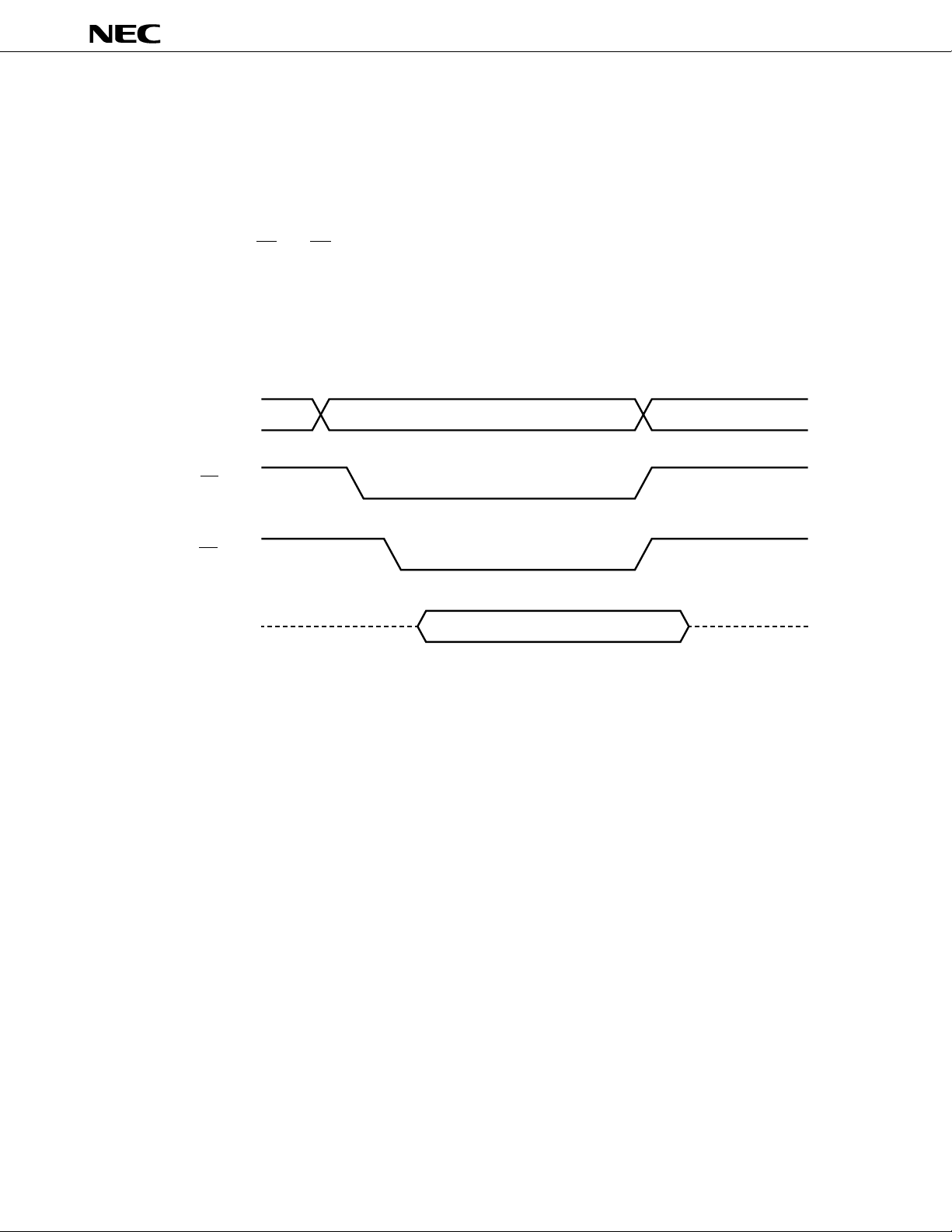
4.4 PROCEDURE FOR READING FROM PROM
The following is a procedure for reading out the contents of PROM to the external data bus (D0 to D7).
(1) Always set each pin as follows: MODE0/V
CONFIGURATION (2).
(2) Apply +5 V to the VDD and MODE0/VPP pins.
(3) Input the address of data to be read into the A0 to A16 pins.
(4) Read mode (CE = L, OE = L)
(5) Output the data on the D0 to D7 pins.
Fig. 4-5 is a timing chart of these steps (2) to (5).
Fig. 4-5 PROM Read Timing Chart
A0 - A16
CE (input)
OE (input)
PP = H and MODE1 = L. Connect unused pins according to PIN
Address input
D0 - D7
Hi-Z Hi-Z
Data output
21
Page 22

m
PD78P368A
5. ERASURE CHARACTERISTICS (mPD78P368AKL-S ONLY)
Data written in the mPD78P368AKL-S program memory can be erased (FFH); therefore users can write other data
in the memory.
To erase the written data, expose the erasure window to light with a wavelength shorter than approx. 400 nm. Normally,
ultraviolet light with a wavelength of 254 nm is employed. The amount of light required to completely erase the data
is as follows:
2
• Intensity of ultraviolet light ¥ erasing time: 15 W•s/cm
• Erasing time: 15 to 20 minutes (When using a 12,000
due to lamp deterioration, dirt on the erasure window, or the like.)
The ultraviolet lamp should be placed within 2.5 cm from the erasure window during erasure. In addition, if a filter
is attached to the ultraviolet lamp, remove the filter before erasure.
min.
m
W/cm2 ultraviolet lamp. It may, however, take more time
6. PROTECTIVE FILM COVERING THE ERASURE WINDOW (
After the erasure window of the mPD78P368AKL-S has been exposed to sunlight or a fluorescent lamp for a long
time, data in EPROM may be erased and the internal circuits may malfunction. To prevent these failures, the erasure
window should be covered with a protective film when it is not used for erasure.
EPROM package products with a window are supplied with a NEC-guaranteed protective film when they are
delivered.
mm
m
PD78P368AKL-S ONLY)
mm
7. SCREENING ONE-TIME PROM PRODUCTS
NEC cannot execute a complete test of one-time PROM products (mPD78P368AGF-3B9) due to their structure
before shipment. It is recommended that you screen (verify) PROM products after writing necessary data into them
and storing them at 125 °C for 24 hours.
NEC offers a charged service called QTOP
PROM, marking, screening, and verification. Ask your sales representative for details.
microcomputer service. This service includes writing to one-time
22
Page 23

m
PD78P368A
8. ELECTRICAL SPECIFICATIONS
ABSOLUTE MAXIMUM RATINGS (TA = 25 °C)
Parameter Symbol Conditions Rating Unit
Power supply voltage V DD –0.5 to +7.0 V
AVDD –0.5 to VDD + 0.5 V
VPP –0.5 to +13.5 V
AVSS –0.5 to +0.5 V
Input voltage VI Pins other than –0.5 to VDD + 0.5 V
P70/ANI0-P77/ANI7
Output voltage VO –0.5 to VDD + 0.5 V
Low-level output current IOL
High-level output current IOH All output pins –3.0 mA
Analog input voltage VIAN P70/ANI0-P77/ANI7 pins AVSS – 0.5 to AVDD + 0.5 V
A/D converter reference input voltage AVREF AVSS – 0.5 to AVDD + 0.5 V
Operating ambient temperature TA –40 to +85 °C
Storage temperature Tstg –60 to +150 °C
Note
Output pins other than 4.0 mA
those in the note
Total of all output pins 200 mA
Total of all output pins –25 mA
20 mA
H
Note P00/RTP0-P03/RTP3, P04/PWM0, P05/TCUD/PWM1, P06/TIUD/TO40, P07/TCLRUD, P10-P17, and
P80/TO00-P85/TO05 pins.
Caution Absolute maximum ratings are rated values beyond which some physical damages may be
caused to the product; if any of the parameters in the table above exceeds its rated value even
for a moment, the quality of the product may deteriorate. Be sure to use the product within the
rated values.
RECOMMENDED OPERATING CONDITIONS
Oscillation frequency TA VDD
3 MHz - fXX - 8 M Hz –40 to +85 °C +5.0 V ±10 %
CAPACITANCE (TA = 25 °C, VSS = VDD = 0 V)
Parameter Symbol Conditions Min. Typ. Max. Unit
Input capacitance CI f = 1 MHz 20 pF
Output capacitance CO 0 V except measured pins 20 pF
I/O capacitance CIO 20 pF
23
Page 24

m
PD78P368A
OSCILLATOR CHARACTERISTICS (TA = –40 to +85 °C, VDD = +5 V ±10 %, VSS = 0 V)
Resonator Recommended circuit Parameter Min. Max. Unit
Ceramic resonator or Oscillation frequency (fXX) 3 8 MHz
crystal
External clock X1 input frequency (fX) 3 8 MHz
V
SS
C1 C2
X2X1
X1 X2
Open
HCMOS
inverter
X1 rise/fall time (tXR, tXF)030ns
X1 input high-/low-level 40 170 ns
width (tWXH, tWXL)
Caution When using system clock oscillation circuits, to reduce the effect of the wiring capacitance,
etc, wire the area indicated by dotted-line as follows:
• Make the wiring as short as possible.
• Do not allow the wiring to intersect other signal lines. Keep it away from other lines in which
varying high currents flow.
• Make sure that the ground point of the oscillation circuit capacitor is always at the same electric
potential as V
SS. Do not allow the wiring to be grounded to a ground pattern in which very high
currents are flowing.
• Do not extract signals from the oscillation circuit.
24
Page 25

m
PD78P368A
DC CHARACTERISTICS (TA = –40 to +85 °C, VDD = +5 V ±10 %, VSS = 0 V)
Parameter Symbol Conditions Min. Typ. Max. Unit
Low-level input voltage VIL1
VIL2
High-level input voltage VIH1
VIH2
Low-level output voltage VOL1
VOL2
VOL3
High-level output voltage VOH IOH = –400 mA
Input leakage current ILI 0 V - VI - VDD, AVDD = VDD ±10
Output leakage current ILO 0 V - VO - VDD, AVDD = VDD ±10
VDD supply current IDD1 Operating mode 70 120 mA
IDD2 HALT mode 45 70 mA
Data retention voltage VDDDR STOP mode 2.5 V
Data retention current IDDDR STOP mode VDDDR = 2.5 V 2 10
Pull-up resistance RL VI = 0 V 15 60 150 K ý
Note 1
Note 2
Note 1
Note 2
Note 3
Note 4
Note 5
0 0.8 V
0 0.2VDD V
2.2 V
0.8VDD V
IOL = 2.0 mA 0.45 V
IOL = 15 mA 1.5 V
IOL = 10 mA 1.5 V
VDD – 1.0
VDDDR = 5.0 V ±10 % 10 50
V
m
A
m
A
m
A
m
A
Notes 1. Pins other than those specified in Note 2.
2. RESET, X1, X2, P20/NMI, P21/INTP0, P22/INTP1, P23/INTP2, P24/INTP3/TI, P25/INTP4, P32/SO/
SB0, P33/SI/SB1 and P34/SCK pins.
3. Pins other than those specified in Notes 4 and 5.
4. P80/TO00-P85/TO05 pins (When IOL = 15 mA is in operation, up to three pins can be ON simultane-
ously.)
5. P00/RTP0-P03/RTP3, P04/PWM0, P05/TCUD/PWM1, P06/TIUD/TO40 and P07/TCLRUD pins (When
OL = 10 mA is in operation, up to four pins can be ON simultaneously.) as well as P10-P17 pins (When
I
OL = 10 mA is in operation, up to four pins can be ON simultaneously.).
I
Caution When the P80-P85, P00-P07, and P10-P17 pins are not used under the conditions specified in
Notes 4 and 5, they have the same characteristics as in Note 3.
25
Page 26

m
PD78P368A
AC CHARACTERISTICS (TA = –40 to +85 °C, VDD = +5 V ±10 %, VSS = 0 V, CL = 100 pF, fXX = 8 MHz)
Read/Write Operation (when general-purpose memory is connected)
Parameter Symbol Conditions Min. Max. Unit
System clock cycle time tCYK 62.5 166.7 ns
Address setup time (vs. ASTB Ø)tSAST 7ns
Address hold time (vs. ASTB Ø)tHSTA 11 ns
RD Ø Æ address float time tFRA 24 ns
Address Æ data input time tDAID 100 ns
RD Ø Æ data input time tDRID 49 ns
ASTB Ø Æ RD Ø delay time tDSTR 15 ns
Data hold time (vs. RD •)tHRID 0ns
RD • Æ address active time tDRA 17 ns
RD low-level width tWRL 63 ns
ASTB high-level width tWSTH 14 ns
WR Ø Æ data output time tDWOD 21 ns
ASTB Ø Æ WR Ø delay time tDSTW 15 ns
WR • Æ ASTB • delay time tDWST 78 ns
Data setup time (vs. WR •)tSODW 57 ns
Data hold time (vs. WR •)tHWOD 8ns
WR low-level width tWWL 63 ns
tCYK-dependent Bus Timing Definition
Parameter Arithmetic expression Min./Max. Unit
tSAST (0.5 + a) T – 24 Min. ns
tHSTA 0.5T – 20 Min. ns
tWSTH (0.5 + a) T – 17 Min. ns
tDSTR 0.5T – 16 Min. ns
tWRL (1.5 + n) T – 30 Min. ns
tDAID (2.5 + a + n) T – 56 Max. ns
tDRID (1.5 + n) T – 44 Max. ns
tDRA 0.5T – 14 Min. ns
tDSTW 0.5T – 16 Min. ns
tDWST 1.5T – 15 Min. ns
tWWL (1.5 + n) T – 30 Min. ns
tDWOD 0.5T – 10 Max. ns
tSODW (1 + n) T – 5 Min. ns
Remarks1. T = tCYK = 1/fCLK (fCLK refers to the internal system clock frequency.)
2. a becomes 1 when the address wait is inserted. Otherwise, it becomes 0.
3. n refers to the number of wait cycles that is inserted by specifying the PWC register.
4. Only the bus timings indicated in this table depend on t
CYK.
26
Page 27

m
PD78P368A
SERIAL OPERATION (TA = –40 to +85 °C, VDD = +5 V ±10 %, VSS = 0 V)
Parameter Symbol Conditions Min. Max. Unit
Serial clock cycle time tCYSK SCK output Internal 8 dividing 500 ns
SCK input External clock 500 ns
Serial clock low-level width tWSKL SCK output Internal 8 dividing 210 ns
SCK input External clock 210 ns
Serial clock high-level width tWSKH SCK output Internal 8 dividing 210 ns
SCK input External clock 210 ns
SI setup time (vs. SCK •)
tSRXSK 80 ns
SI hold time (vs. SCK •)tHSKRX 80 ns
SCK Ø Æ SO delay time tDSKTX R = 1 ký, C = 100 pF 210 ns
UP/DOWN COUNTER OPERATION (TA = –40 to +85 °C, VDD = +5 V ±10 %, VSS = 0 V)
Parameter Symbol Conditions Min. Max. Unit
TIUD high-/low-level width
TCUD high-/low-level width
TCLRUD high-/low-level width
TCUD setup time (vs. TIUD •)
TCUD hold time (vs. TIUD •)
TIUD setup time (vs. TCUD)
TIUD hold time (vs. TCUD)
TIUD & TCUD cycle time
t
WTIUH
, t
WTIUL
Other than mode 4 2T ns
Mode 4 4T ns
t
WTCUH
, t
WTCUL
Other than mode 4 2T ns
Mode 4 4T ns
t
WCLUH
, t
WCLUL
2T ns
tSTCU Mode 3 T ns
tHTCU Mode 3 T ns
tS4TIU Mode 4 2T ns
tH4TIU Mode 4 2T ns
tCYC Other than mode 4 4 MHz
tCYC4 Mode 4 2 MHz
Remark T = tCYK = 1/fCLK (fCLK refers to the internal system clock frequency.)
27
Page 28

m
PD78P368A
OTHER OPERATIONS (TA = –40 to +85 °C, VDD = +5 V ±10 %, VSS = 0 V)
Parameter Symbol Conditions Min. Max. Unit
NMI high-/low-level width tWNIH, tWNIL 2
RESET high-/low-level width
INTP0 high-/low-level width tWI0H, tWI0L Ts = T 250 ns
INTP1 high-/low-level width tWI1H, tWI1L Ts = T 250 ns
INTP2 high-/low-level width tWI2H, tWI2L Ts = T 250 ns
INTP3(TI) high-/low-level width tWI3H, tWI3L Ts = T 250 ns
INTP4 high-/low-level width tWI4H, tWI4L Ts = T 250 ns
t
WRSH
, t
WRSL
Ts = 4T 1.0
Ts = 8T 2.0
Ts = 16T 4.0
Ts = 4T 1.0
Ts = 8T 2.0
Ts = 16T 4.0
Ts = 4T 1.0
Ts = 4T 1.0
Ts = 8T 2.0
Ts = 16T 4.0
Ts = 64T 16.0
Ts = 128T 32.0
Ts = 256T 64.0
Ts = 4T 1.0
Ts = 8T 2.0
Ts = 16T 4.0
1.5
m
s
m
s
m
s
m
s
m
s
m
s
m
s
m
s
m
s
m
s
m
s
m
s
m
s
m
s
m
s
m
s
m
s
m
s
Remarks1. T = tCYK = 1/fCLK (fCLK refers to the internal system clock frequency.)
2. Ts refers to the input sampling frequency. INTP0-INTP4 can be selected to programmable.
28
Page 29

m
PD78P368A
A/D CONVERTER CHARACTERISTICS (TA = –40 to +85 °C, VDD = +5 V ±10 %, VSS = AVSS = 0 V,
V
DD – 0.5 V - AVDD - VDD)
Parameter Symbol Conditions Min. Typ. Max. Unit
Resolution 10 bit
Total error
Quantization error ±1/2 LSB
Conversion time tCONV 62.5 ns - tCYK < 80 ns 208 tCYK
Sampling time tSAMP 62.5 ns - tCYK < 80 ns 8 tCYK
Zero-scale error
Full-scale error
Nonlinearity error
Analog input voltage
Analog input impedance RAN When not sampling 10 MW
Reference voltage A VREF 3.4 AVDD V
AVREF1 current AIREF 1.0 3.0 mA
AVDD supply current AIDD Operating mode 2.0 6.0 mA
A/D converter data AIDDDR STOP mode AVDDDR = 2.5 V 2 10
retention current
Note 1
Note 1
Note 1
Note 1
Note 2
4.5 V - AVREF - AVDD ±0.4 %FSR
3.4 V - AVREF - AVDD ±0.7 %FSR
80 ns - tCYK - 166.6 ns 169 tCYK
80 ns - tCYK - 166.6 ns 6 tCYK
4.5 V - AVREF - AVDD ±1.5 ±2.5 LSB
3.4 V - AVREF - AVDD ±1.5 ±4.5 LSB
4.5 V - AVREF - AVDD ±1.5 ±2.5 LSB
3.4 V - AVREF - AVDD ±1.5 ±4.5 LSB
4.5 V - AVREF - AVDD ±1.5 ±2.5 LSB
3.4 V - AVREF - AVDD ±1.5 ±4.5 LSB
VIAN –0.3
When sampling
AVDDDR = 5 V ±10 % 10 50
AVREF + 0.3
Note 3
V
m
A
m
A
Notes 1. The quantization error is excluded.
2. When –0.3 V - V
When 0 V < V
When AV
REF - VIAN - AVREF + 0.3 V, the conversion result becomes 3FFH.
IAN - 0 V, the conversion result becomes 000H.
IAN < AVREF, the conversion is performed with the 10-bit resolution.
3. The analog input impedance at the time of sampling is the same as the equivalent circuit shown below.
(The values in the diagram are TYP. values; they are not guaranteed values.)
1 k
Analog input pin
Ω
25 pF
(Input
capacitance
included)
1.4 pF
29
Page 30

m
PD78P368A
Cautions 1. When using the P70/ANI0-P77/ANI7 pins for both digital and analog inputs, the previously
described characteristics are not guaranteed. Therefore, ensure that all of the eight P70/
ANI0-P77/ANI7 pins are used either for analog input or digital input.
2. When using the P70/ANI0-P77/ANI7 pins as digital input, make sure to set that AV
and AV
SS = VSS.
DD = VDD,
AC Timing Test Point
DD
V
0 V
0.8VDD or 2.2 V
DD
or 0.8 V
0.2V
Test point
0.8V
0.2V
DD
or 2.2 V
DD
or 0.8 V
30
Page 31

Read Operation
(CLK)
m
PD78P368A
t
CYK
A8 - A15
(output)
AD0 - AD7
(input/output)
ASTB
(output)
RD
(output)
Write Operation
(CLK)
High-order address High-order address
t
t
DSTR
t
HSTA
DAID
Data (input)
t
FRA
t
DRID
t
WRL
t
DRA
Low-order address (output)
t
HRID
t
SAST
Hi-Z Hi-Z Hi-Z Hi-Z
Low-order address (output)
t
WSTH
A8 - A15
(output)
AD0 - AD7
(output)
ASTB
(output)
WR
(output)
High-order address High-order address
t
SAST
Low-order address (output)
t
WSTH
t
HSTA
t
DSTW
Undefined
t
DWOD
t
WWL
Data (output)
t
SODW
t
HWOD
t
DWST
Low-order address (output)
31
Page 32

Serial Operation
SCK
t
DSKTX
SO
SI
Up/Down Counter (Timer 4) Input Timing
t
t
SRXSK
WSKL
t
CYSK
t
WSKH
t
HSKRX
m
PD78P368A
TIUD
TCUD
TCLRUD
tSTCU
tWTIUH
tWTIUL
tHTCU
tWTCUL
tWTCUH
tWCLUH
tWCLUL
32
TIUD
tS4TIU tH4TIU tS4TIU tH4TIU
TCUD
Page 33

Interrupt Input Timing
NMI
INTPn
Remark n = 0 – 4
Reset Input Timing
t
WNIH
t
WInH
0.8V
0.8V
DD
0.2V
DD
0.2V
m
PD78P368A
t
WNIL
DD
t
WInL
DD
RESET
t
WRSH
0.8V
DD
0.2V
t
WRSL
DD
33
Page 34

DC PROGRAMMING CHARACTERISTICS (TA = 25 ±5 °C, VSS = 0 V)
m
PD78P368A
Parameter
High-level input
voltage
Low-level input
voltage
Input leakage current
High-level output
voltage
Low-level output
voltage
Output leakage
current
VDDP supply voltage
VPP supply voltage
VDDP supply current
VPP supply current
Symbol
VIH
VIL
ILIP
VOH
VOL
ILO
VDDP
VPP
IDD
IPP
Symbol
VOH
VOL
VCC
VPP
VIH
VIL
ILI
–
IDD
IPP
Note 1
Conditions
0 - VI - VDDP
IOH = –400 mA
IOL = 2.1 mA
0 - VO - VDDP, OE = VIH
Program memory write mode
Program memory read mode
Program memory write mode
Program memory read mode
Program memory write mode
Program memory read mode
Program memory write mode
Program memory read mode
Note 2
Min.
2.4
–0.3
2.4
6.25
4.5
12.2
VDD – 0.6
Typ.
6.5
5.0
12.5
VDD
Max.
VDDP + 0.3
0.8
±10
0.45
±10
6.75
5.5
12.8
VDD + 0.6
50
50
50
100
Unit
V
V
m
A
V
V
m
A
V
V
V
V
mA
mA
mA
m
A
Notes 1. Symbols for the corresponding mPD27C1001A
2. The V
DDP represents the VDD pin as viewed in the programming mode.
34
Page 35

AC PROGRAMMING CHARACTERISTICS (TA = 25 ±5 °C, VSS = 0 V)
PROM Write Mode (Page Program Mode)
m
PD78P368A
Parameter
Address set up time
CE set time
Input data setup time
Address hold time
Input data hold time
Output data hold time
VPP setup time
VDDP setup time
Initial program pulse width
OE set time
Valid data delay time from OE
OE pulse width in the data latch
PGM setup time
CE hold time
OE hold time
Symbol
tCES
tAHL
tAHV
tDH
tVPS
tVDS
tPW
tOES
tOE
tLW
tPGMS
tCEH
tOEH
Note 1
tAS
tDS
tAH
tDF
Note 2
Conditions
Min.
2
2
2
2
2
0
2
0
1
1
0.095
2
1
2
2
2
Typ. Max.
250
0.105
1.0
Unit
m
m
m
m
m
m
m
ns
ms
ms
ms
m
m
m
m
m
m
s
s
s
s
s
s
s
s
s
s
s
s
s
Notes 1. These symbols (except tVDS) correspond to those of the mPD27C1001A.
2. For
m
PD27C1001A, read tVDS as tVCS.
35
Page 36

PROM Write Mode (Byte Program Mode)
m
PD78P368A
Parameter
Address set up time
CE set time
Input data setup time
Address hold time
Input data hold time
Output data hold time
VPP setup time
VDDP setup time
Initial program pulse width
OE set time
Valid data delay time from OE
Symbol
tAS
tCES
tDS
tAH
tDH
tDF
tVPS
Note 2
tVDS
tPW
tOES
tOE
Note 1
Conditions
Min.
2
2
2
2
2
0
1
1
0.095
2
Notes 1. These symbols (except tVDS) correspond to those of the mPD27C1001A.
m
2. For
PD27C1001A, read tVDS as tVCS.
PROM Read Mode
Parameter
Data output time from address
CE Ø Æ data output time
OE Ø Æ data output time
Data hold time to OE •
Data hold time to address
Symbol
tACC
tCE
tOE
tDF
tOH
Note
Conditions
CE = OE = VIL
OE = VIL
CE = VIL
CE = VIL
CE = OE = VIL
Min.
0
0
Typ. Max.
250
0.105
1.0
Typ. Max.
1.0
1.0
1.0
250
Unit
m
m
m
m
m
ns
ms
ms
ms
m
m
Unit
m
m
m
ns
ns
s
s
s
s
s
s
s
s
s
s
Note These symbols correspond to those of the
m
PD27C1001A.
36
Page 37

PROM Write Mode Timing (Page Program Mode)
Page data latch Page program Program verify
A2 - A16
t
V
V
DDP
CE
PGM
OE
PP
A0, A1
D0 - D7
V
DDP
V
V
DDP
+ 1.5
DDP
V
V
V
V
V
V
V
AS
t
DS
Hi-Z Hi-ZHi-Z
t
VPS
PP
t
VDS
IH
IL
IH
IL
IH
IL
t
LW
t
AHL
t
DH
Data input
t
PGMS
m
PD78P368A
t
AHV
t
DF
Data
t
OE
output
t
CES
t
CEH
t
PW
t
OES
t
t
OEH
AH
37
Page 38

PROM Write Mode Timing (Byte Program Mode)
Program Program verify
A0 - A16
t
AS
m
PD78P368A
t
DF
D0 - D7
V
PP
V
V
DDP
+ 1.5
V
DDP
V
Hi-Z Hi-ZHi-Z
t
DS
PP
V
DDP
DDP
V
IH
t
t
VPS
VDS
Data input Data output
t
DH
CE
V
IL
V
IH
t
CES
t
PW
PGM
V
IL
V
IH
t
OES
t
OE
OE
V
IL
Cautions 1. VDDP must be applied before VPP, and must be cut after VPP.
PP including overshoot must not exceed +13.5 V.
2. V
3. Plugging in or out the board with the V
PP pin supplied with +12.5 V may adversely affect its
reliability.
t
AH
PROM Read Mode Timing
A0 - A16
CE
OE
D0 - D7
Notes 1. For reading within t
DF is the time measured from when either OE or CE reaches VIH, whichever is faster.
2. t
38
Valid address
t
CE
Note 2
t
Note 1
t
ACC
Hi-Z Hi-Z
ACC, the delay of the OE input from falling edge of CE must be within tACC – tOE.
Note 1
t
OE
t
OH
Data output
DF
Page 39

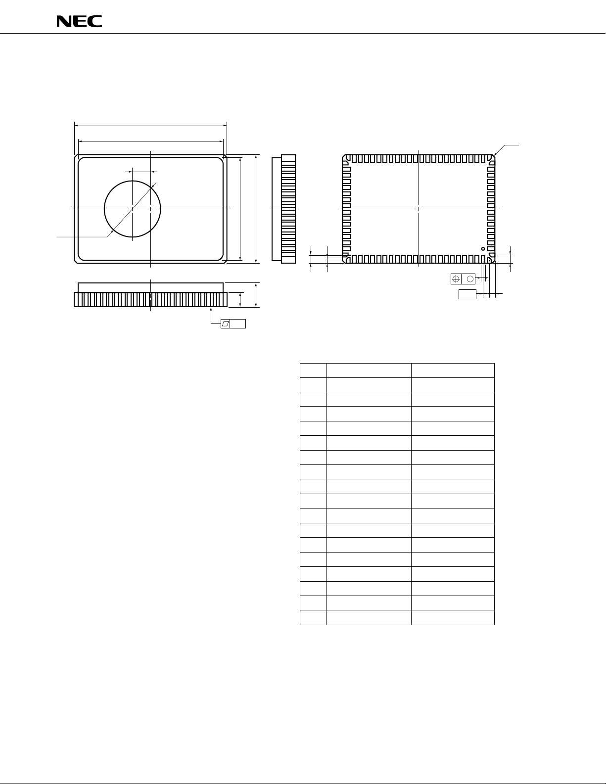
9. PACKAGE DRAWINGS
80 PIN PLASTIC QFP (14
20)
NOTE
Each lead centerline is located within 0.15 mm (0.006 inch) of
its true position (T.P.) at maximum material condition.
detail of lead end
M
F
G
H
I
J
K
M
L
N
P
Q
R
ITEM MILLIMETERS INCHES
S
P80GF-80-3B9-3
3.0 MAX. 0.119 MAX.
K 1.8±0.2 0.071
+0.008
–0.009
L 0.8±0.2 0.031
+0.009
–0.008
P 2.7
0.106
N 0.10 0.004
M 0.15 0.006
+0.004
–0.003
Q 0.1±0.1 0.004±0.004
A 23.6±0.4 0.929±0.016
B 20.0±0.2 0.795
+0.009
–0.008
C 14.0±0.2 0.551
+0.009
–0.008
G
F
0.8
1.0
0.031
0.039
D 17.6±0.4 0.693±0.016
J 0.8 (T.P.) 0.031 (T.P.)
I 0.15 0.006
H 0.35±0.10 0.014
+0.004
–0.005
+0.10
–0.05
64
65
40
80
1
25
24
41
A
B
CD
S
R5°±5° 5°±5°
m
PD78P368A
39
Page 40
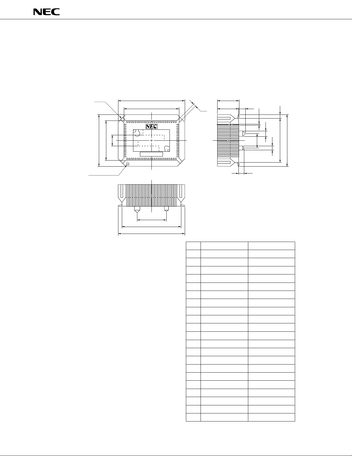
80 PIN CERAMIC WQFN
A
B
U1
T
C
D
G
F
m
PD78P368A
Q
80
S
K
W
HI
1
M
JR
Z
NOTE
Each lead centerline is located within 0.08
mm (0.003 inch) of its true position (T.P.) at
maximum material condition.
X80KW-80A1
ITEM MILLIMETERS INCHES
A
B
C
D
F
G
H
J
K
Q
R
S
T
U1
W
Z
20.0±0.25
19.0
13.4
14.2±0.2
1.84
3.56MAX.
0.51±0.1
I
0.08
0.8 (T.P.)
1.0±0.15 0.039
C0.3
0.8 0.031
1.1 0.043
φφ
7.62
2.6
0.75±0.15 0.03
0.10
+0.011
0.787
–0.010
0.748
0.528
0.559±0.008
0.072
0.141MAX.
0.02±0.004
0.003
0.031 (T.P.)
+
0.007
–
0.006
C0.012
0.3
0.102
+0.006
–
0.007
0.004
40
Page 41

m
PD78P368A
10. RECOMMENDED SOLDERING CONDITIONS
These products should be soldered and mounted under the conditions recommended below.
For details of recommended soldering conditions, refer to the information document
Mounting Technology Manual
(C10535J).
For soldering methods and conditions other than those recommended, please contact your NEC sales
representative.
Table 10-1. Surface Mount Type Soldering Conditions
m
PD78P368AGF-3B9: 80-Pin Plastic QFP (14 ¥ 20 mm)
Soldering method
Infrared reflow
VPS
Wave soldering
Partial heating
Package peak temperature: 235 °C, Duration: 30 sec. max. (210 °C or above)
Number of times: 2 max.
Exposure limit: 7 days
afterward)
<Caution>
Non-heat-resistant trays, such as magazine and taping trays, cannot be baked
before unpacking.
Package peak temperature: 215 °C, Duration: 40 sec. max. (200 °C or above)
Number of times: 2 max.
Exposure limit: 7 days
afterward)
<Caution>
Non-heat-resistant trays, such as magazine and taping trays, cannot be baked
before unpacking.
Solder bath temperature: 260 °C or less, Time: 10 sec. max.,
Number of times: 1, Pre-heating temperature: 120 °C max. (Package surface
temperature)
Exposure limit: 7 days
afterward)
Pin temperature: 300 °C or less
Duration: 3 sec. max. (per side of device)
Soldering conditions
Note
(20 hours of pre-baking is required at 125 °C
Note
(20 hours of pre-baking is required at 125 °C
Note
(20 hours of pre-baking is required at 125 °C
Semiconductor Device
Recommended
condition symbol
IR35-207-2
VP15-207-2
WS60-207-1
–
H
Note Maximum number of days during which the product can be stored at a temperature of 25 °C and a relative
humidity of 65 % or less after dry-pack package is opened.
Caution Use of more than one soldering method should be avoided (except in the case of partial heating).
41
Page 42

APPENDIX A TOOLS
A.1 DEVELOPMENT TOOLS
The following tools are provided for developing a system that uses the
Language processor
m
PD78P368A:
m
PD78P368A
78K/III series relocatable assembler
(RA78K3)
78K/III series C compiler
(CC78K3)
This relocatable program can be used for all 78K/III series emulators. With its
macro functions, it allows the user to improve program development efficiency.
A structured-programming assembler is also provided, which enables explicit
description of program control structures. This assembler could improve productivity in program production and maintenance.
Host machine
PC-9800 series
IBM PC/ATTM or
compatibles
HP9000 series
TM
700
SPARCstation
NEWS
This C compiler can be used for all 78K/III series emulators. The compiler
converts programs written in C language into object codes executable on the
microcomputer. When the compiler is used, the 78K/III series relocatable
assembler package (RA78K3) is needed.
Host machine
PC-9800 series
IBM PC/AT or
compatibles
HP9000 series
700
SPARCstation
NEWS
TM
TM
MS-DOS
PC DOS
HP-UX
SunOS
NEWS-OS
OS
MS-DOS
PC DOS
TM
HP-UX
TM
SunOS
NEWS-OS
OS
TM
TM
TM
Distribution media
3.5-inch 2HD
5.25-inch 2HD
3.5-inch 2HC
5.25-inch 2HC
DAT
Cartridge tape
(QIC-24)
Distribution media
3.5-inch 2HD
5.25-inch 2HD
3.5-inch 2HC
5.25-inch 2HC
DAT
Cartridge tape
(QIC-24)
Part number
m
S5A13RA78K3
m
S5A10RA78K3
m
S7B13RA78K3
m
S7B10RA78K3
m
S3P16RA78K3
m
S3K15RA78K3
m
S3R15RA78K3
Part number
m
S5A13CC78K3
m
S5A10CC78K3
m
S7B13CC78K3
m
S7B10CC78K3
m
S3P16CC78K3
m
S3K15CC78K3
m
S3R15CC78K3
Remark It is guaranteed that the relocatable assembler and C compiler run only under the OSs on the
corresponding host machines described above.
42
Page 43

PROM programming tools
m
PD78P368A
Hardware
Software
PG-1500
PA-78P368GF
PA-78P368KL
PG-1500 controller
The PG-1500 PROM programmer is used together with an accessory board and
optional program adapter. It allows the user to program a single chip microcomputer containing PROM independently or from a host machine. The PG-1500 can
be used to program typical 256K-bit to 4M-bit PROMs.
Programmer adapter for writing programs to the mPD78P368A. Used with a
PROM programmer such as the PG-1500.
PA-78P368GF : For mPD78P368AGF
PA-78P368KL : For mPD78P368AKL
This program enables the host machine to control the PG-1500 through the serial
and parallel interfaces.
Host machine
PC-9800 series
IBM PC/AT or
compatibles
MS-DOS
PC DOS
OS
Distribution media
3.5-inch 2HD
5.25-inch 2HD
3.5-inch 2HC
5.25-inch 2HC
Part number
m
S5A13PG1500
m
S5A10PG1500
m
S7B13PG1500
m
S7B10PG1500
Remark It is guaranteed that the PG-1500 controller runs only under the OSs on the corresponding host machines
described above.
Debugging tools (when the IE controller is used)
Hardware
Software
IE-78350-R
IE-78365-R-EM1
EP-78365GF-R
EV-9200G-80
IE-78350-R control program
(IE controller)
In-circuit emulator for developing and debugging an application system. For
debugging, connect the emulator to the host machine.
I/O emulation board for emulating peripheral hardware such as the I/O ports
of the target device.
Emulation probe for connecting the IE-78350-R to the target system.
One EV-9200G-80 conversion socket is provided for connection to the target
system.
This control program allows the user to control the IE-78350-R from the host
machine. Its automatic command execution function ensures more efficient
debugging.
Host machine
PC-9800 series
IBM PC/AT or
compatibles
OS
MS-DOS
PC DOS
Distribution media
3.5-inch 2HD
5.25-inch 2HD
3.5-inch 2HC
5.25-inch 2HC
Part number
m
S5A13IE78365A
m
S5A10IE78365A
m
S7B13IE78365A
m
S7B10IE78365A
Remark It is guaranteed that the IE controller runs only under the OSs on the corresponding host machines
described above.
H
H
H
H
43
Page 44

Configuration of development tools (when the IE controller is used)
Host machine:
PC-9800 series
IBM PC/AT
EWS
Software
RS-232-C
IE-78350-R
in-circuit emulator
+
IE-78365-R-EM1
I/O emulation board
(option)
RS-232-C
m
PD78P368A
Emulation probe
Relocatable
assembler
IE controller
Device containing PROM
Programmer adapter
C compiler PG-1500
µµ
PD78P368AGF
controller
PD78P368AKL
++
PA-78P368KLPA-78P368GF
PG-1500
Note The socket is supplied with the emulation probe.
PROM programmer
EP-78365GF-R
+
Socket for connecting the
emulation probe and target
Note
system
EV-9200G-80
Target system
Remarks 1. The PG-1500 can be directly connected to the host machine via the RS-232-C interface.
2. In this figure, the distribution media of software is represented by the 3.5-inch floppy disk.
44
Page 45

Debugging tools (when the integrated debugger is used)
m
PD78P368A
Hardware
Software
IE-784000-R
IE-78350-R-EM-A
IE-78365-R-EM1
EP-78365GF-R
IE-70000-98-IF-B
IE-70000-98N-IF
IE-70000-PC-IF-B
IE-78000-R-SV3
Integrated debugger
(ID78K3)
Note
EV-9200G-80
In-circuit emulator for developing and debugging an application system. For
debugging, connect the emulator to the host machine.
Emulation board for emulating peripheral hardware such as the I/O ports of the
target device.
I/O emulation board for emulating peripheral hardware such as the I/O ports of
the target device.
Emulation probe for connecting the IE-784000-R to the target system. One EV9200G-80 conversion socket is provided for connection to the target system.
Interface adapter when the PC-9800 series computer (other than a notebook) is
used as the host machine.
Interface adapter and cable when a PC-9800 series notebook is used as the host
machine.
Interface adapter when the IBM PC/AT is used as the host machine.
Interface adapter and cable when the EWS is used as the host machine.
Program for controlling the in-circuit emulator for the 78K/III series. The inte-
grated debugger (ID78K3) is used together with the device file (DF78365).
Debugging can be performed for the source program written in C, structured
assembly language, or assembly language. The ID78K3 can display various
information simultaneously on the host machine screen divided into multiple
areas. This ensures efficient debugging.
Device file (DF78365)
Host machine
OS
PC-9800 series
IBM PC/AT or
compatibles
(Japanese Windows)
IBM PC/AT or
compatibles
(Windows)
File which contains the device-specific information. The device file (DF78365) is
used together with the assembler (RA78K3), C compiler (CC78K3), or integrated
debugger (ID78K3).
Host machine
PC-9800 series
IBM PC/AT or
compatibles
MS-DOS
+
Windows
PC DOS
+
Windows
OS
MS-DOS
PC DOS
Distribution media
3.5-inch 2HD
TM
5.25-inch 2HD
3.5-inch 2HC
5.25-inch 2HC
3.5-inch 2HC
5.25-inch 2HC
Distribution media
3.5-inch 2HD
5.25-inch 2HD
3.5-inch 2HC
5.25-inch 2HC
Part number
m
SAA13ID78K3
m
SAA10ID78K3
m
SAB13ID78K3
m
SAB10ID78K3
m
SBB13ID78K3
m
SBB10ID78K3
Part number
m
S5A13DF78365
m
S5A10DF78365
m
S7B13DF78365
m
S7B10DF78365
Note Under development
Remark It is guaranteed that the integrated debugger and device file run only under the OSs on the corresponding
host machines described above.
45
Page 46

Configuration of development tools (when the integrated debugger is used)
m
PD78P368A
Host machine:
PC-9800 series
IBM PC/AT
EWS
Software
Relocatable
assembler
Integrated
debugger
Device containing PROM
C compiler
Device file
IE-70000-98-IF-B
IE-70000-98N-IF
IE-70000-PC-IF-B
PG-1500
controller
RS-232-C
IE-784000-R
in-circuit emulator
+
IE-78350-R-EM-A
emulation board
(option)
+
IE-78365-R-EM1
I/O emulation board
(option)
PROM programmer
PG-1500
Emulation probe
EP-78365GF-R
Socket for connecting the
emulation probe and target
Note
system
EV-9200G-80
+
µµ
PD78P368AGF
Programmer adapter
PD78P368AKL
++
Target system
PA-78P368KLPA-78P368GF
Note The socket is supplied with the emulation probe.
Remarks 1. In this figure, the host machine is represented by the desktop personal computer.
2. In this figure, the distribution media of software is represented by the 3.5-inch floppy disk.
46
Page 47

m
PD78P368A
A.2 EMBEDDED SOFTWARE
To improve the efficiency of program development and simplify the maintenance of systems incorporating this
microcontroller, the following embedded software is provided.
Real-time OS
Real-time OS
(RX78K/III)
Note
This operating system was designed to provide a multitasking environment for control
applications that require real-time processing. System performance is improved by using
the idling CPU for other processing.
RX78K/III provides system calls that conform to mITRON specifications.
The RX78K/III package provides the RX78K/III nucleus and a tool (Configurator) that is used
for creating multiple information tables.
Host machine
PC-9800 series
IBM PC/AT or
compatibles
MS-DOS
PC DOS
OS
Distribution media
3.5-inch 2HD
5.25-inch 2HD
3.5-inch 2HC
5.25-inch 2HC
Part number
Undecided
Undecided
Undecided
Undecided
Note Under development
Caution Before purchasing this software, complete the purchase application sheet and sign the software
license agreement.
Remark To use the RX78K/III real-time operating system, the optional RA78K3 assembler package is required.
47
Page 48

Fuzzy inference development support system
m
PD78P368A
Tool for creating fuzzy
knowledge data
(FE9000, FE9200)
Translator
(FT78K3)
Fuzzy inference module
(FI78K/III)
Note
Note
This program supports the input/editing and simulation of fuzzy knowledge data (fuzzy rules
and membership functions).
Host machine
PC-9800 series
IBM PC/AT or
compatibles
This program converts fuzzy knowledge data, obtained using the tool for creating fuzzy
knowledge data, into an assembler source program for RA78K3.
Host machine
PC-9800 series
IBM PC/AT or
compatibles
This program performs fuzzy inference by linking the fuzzy knowledge data converted by
Translator.
Host machine
PC-9800 series
IBM PC/AT or
compatibles
MS-DOS
PC DOS
Windows
MS-DOS
PC DOS
MS-DOS
PC DOS
OS
+
OS
OS
Distribution media
3.5-inch 2HD
5.25-inch 2HD
3.5-inch 2HC
5.25-inch 2HC
Distribution media
3.5-inch 2HD
5.25-inch 2HD
3.5-inch 2HC
5.25-inch 2HC
Distribution media
3.5-inch 2HD
5.25-inch 2HD
3.5-inch 2HC
5.25-inch 2HC
Part number
m
S5A13FE9000
m
S5A10FE9000
m
S7B13FE9200
m
S7B10FE9200
Part number
m
S5A13FT78K3
m
S5A10FT78K3
m
S7B13FT78K3
m
S7B10FT78K3
Part number
m
S5A13FI78K3
m
S5A10FI78K3
m
S7B13FI78K3
m
S7B10FI78K3
Fuzzy inference debugger
(FD78K/III)
Note Under development
This software supports the evaluation and adjustment of fuzzy knowledge data at the
hardware level, by using an in-circuit emulator.
Host machine
PC-9800 series
IBM PC/AT or
compatibles
MS-DOS
PC DOS
OS
Distribution media
3.5-inch 2HD
5.25-inch 2HD
3.5-inch 2HC
5.25-inch 2HC
Part number
m
S5A13FD78K3
m
S5A10FD78K3
m
S7B13FD78K3
m
S7B10FD78K3
48
Page 49
m
PD78P368A
APPENDIX B DIMENSIONS OF THE CONVERSION SOCKET AND RECOMMENDED PATTERN
ON BOARDS
Fig. B-1 Dimensions of the Conversion Socket (EV-9200G-80)(Reference)
Based on EV-9200G-80
(1) Package drawing (in mm)
F
E
C
D
No.1 pin index
1
A
B
EV-9200G-80
H
I
J
N
G
ITEM MILLIMETERS INCHES
A
B
C
D
E
F
G
H
I
J
K
L
M
O
N
P
Q
R
S
T
U
O P
25.0
20.30
4.0
14.45
19.0
4-C 2.8
0.8
11.0
22.0
24.7
5.0
16.2
18.9
8.0
7.8
2.5
2.0
1.35
0.35±0.1
φ
2.3
φ
1.5
S
T
U
K
Q
EV-9200G-80-G0
0.984
0.799
0.157
0.569
0.748
4-C 0.11
0.031
0.433
0.866
0.972
0.197
0.638
0.744
0.315
0.307
0.098
0.079
0.053
+0.004
0.014
–0.005
φ
0.091
φ
0.059
R
L
M
49
Page 50

m
PD78P368A
Fig. B-2 Recommended Pattern on Boards for the Conversion Socket (EV-9200G-80)(Reference)
Based on EV-9200G-80
(2) Pad drawing (in mm)
G
H
L
F
E
D
M
C
B
A
EV-9200G-80-P0
ITEM MILLIMETERS INCHES
A
B
C
D
E
F
G
H
I
J
K
L
M
Caution
25.7
21.0
0.8±0.02 × 23=18.4±0.05
0.8±0.02 × 15=12.0±0.05
15.2
19.9
+0.002
0.031 × 0.906=0.724
–0.001
+0.002
0.031 × 0.591=0.472
–0.001
11.00±0.08
5.50±0.03
5.00±0.08
2.50±0.03
0.5±0.02
φ
2.36±0.03
φ
1.57±0.03
Dimensions of mount pad for EV-9200 and that for target
1.012
0.827
0.598
0.783
0.433
0.217
0.197
0.098
+0.001
0.02
–0.002
φ
0.093
φ
0.062
+0.004
–0.003
+0.001
–0.002
+0.003
–0.004
+0.002
–0.001
+0.001
–0.002
+0.001
–0.002
device (QFP) may be different in some parts. For the
recommended mount pad dimensions for QFP, refer to
"SEMICONDUCTOR DEVICE MOUNTING TECHNOLOGY
MANUAL" (IEI-1207).
J
I
K
+0.003
–0.002
+0.003
–0.002
50
Page 51

m
PD78P368A
Cautions on CMOS Devices
Countermeasures against static electricity for all MOSs
Caution When handling MOS devices, take care so that they are not electrostatically charged.
Strong static electricity may cause dielectric breakdown in gates. When transporting or storing
MOS devices, use conductive trays, magazine cases, shock absorbers, or metal cases that NEC
uses for packaging and shipping. Be sure to ground MOS devices during assembling. Do not
allow MOS devices to stand on plastic plates or do not touch pins.
Also handle boards on which MOS devices are mounted in the same way.
CMOS-specific handling of unused input pins
Caution Hold CMOS devices at a fixed input level.
Unlike bipolar or NMOS devices, if a CMOS device is operated with no input, an intermediatelevel input may be caused by noise. This allows current to flow in the CMOS device, resulting
in a malfunction. Use a pull-up or pull-down resistor to hold a fixed input level. Since unused
pins may function as output pins at unexpected times, each unused pin should be separately
connected to the V
If handling of unused pins is documented, follow the instructions in the document.
DD or GND pin through a resistor.
Statuses of all MOS devices at initialization
Caution The initial status of a MOS device is unpredictable when power is turned on.
Since characteristics of a MOS device are determined by the amount of ions implanted in
molecules, the initial status cannot be determined in the manufacture process. NEC has no
responsibility for the output statuses of pins, input and output settings, and the contents of
registers at power on. However, NEC assures operation after reset and items for mode setting
if they are defined.
When you turn on a device having a reset function, be sure to reset the device first.
QTOP is a trademark of NEC Corporation.
MS-DOS and Windows are trademarks of Microsoft Corporation.
PC/AT and PC DOS are trademarks of IBM Corporation.
HP9000 Series 700 and HP-UX are trademarks of Hewlett-Packard Company.
SPARCstation is a trademark of SPARC International, Inc.
SunOS is a trademark of Sun Microsystems, Inc.
NEWS and NEWS-OS are trademarks of SONY Corporation.
TRON stands for The Realtime Operating system Nucleus.
ITRON stands for Industrial TRON.
51
Page 52

m
PD78P368A
The export of these products from Japan is regulated by the Japanese government. The export of some or all of these
products may be prohibited without governmental license. To export or re-export some or all of these products from a
country other than Japan may also be prohibited without a license from that country. Please call an NEC sales
representative.
License not needed :mPD78P368AKL-S
The customer must judge the need for license :mPD78P368AGF-3B9
No part of this document may be copied or reproduced in any form or by any means without the prior written
consent of NEC Corporation. NEC Corporation assumes no responsibility for any errors which may appear in this
document.
NEC Corporation does not assume any liability for infringement of patents, copyrights or other intellectual
property rights of third parties by or arising from use of a device described herein or any other liability arising
from use of such device. No license, either express, implied or otherwise, is granted under any patents,
copyrights or other intellectual property rights of NEC Corporation or others.
While NEC Corporation has been making continuous effort to enhance the reliability of its semiconductor devices,
the possibility of defects cannot be eliminated entirely. To minimize risks of damage or injury to persons or
property arising from a defect in an NEC semiconductor device, customer must incorporate sufficient safety
measures in its design, such as redundancy, fire-containment, and anti-failure features.
NEC devices are classified into the following three quality grades:
"Standard", "Special", and "Specific". The Specific quality grade applies only to devices developed based on
a customer designated "quality assurance program" for a specific application. The recommended applications
of a device depend on its quality grade, as indicated below. Customers must check the quality grade of each
device before using it in a particular application.
Standard: Computers, office equipment, communications equipment, test and measurement equipment,
audio and visual equipment, home electronic appliances, machine tools, personal electronic
equipment and industrial robots
Special: Transportation equipment (automobiles, trains, ships, etc.), traffic control systems, anti-disaster
systems, anti-crime systems, safety equipment and medical equipment (not specifically designed
for life support)
Specific: Aircrafts, aerospace equipment, submersible repeaters, nuclear reactor control systems, life
support systems or medical equipment for life support, etc.
The quality grade of NEC devices in "Standard" unless otherwise specified in NEC's Data Sheets or Data Books.
If customers intend to use NEC devices for applications other than those specified for Standard quality grade,
they should contact NEC Sales Representative in advance.
Anti-radioactive design is not implemented in this product.
52
M4 94. 11
 Loading...