

Page 1
DATA SHEET
MOS INTEGRATED CIRCUIT
µ
PD3725A
5000-BIT × 3 CCD COLOR LINEAR IMAGE SENSOR
The µPD3725A is a high sensitivity 5000-bit × 3 CCD (Charge Coupled Device) color linear image sensor which
changes optical images to electrical signal and has the function of color separation.
µ
PD3725A has 3 rows of 5000-bit photocell array and 6 rows of 2500-bit charge transferred register, so it is
The
suitable for high resolution color image scanners and digital color copiers.
FEATURES
• Valid photocell : 5000-bit × 3
µ
• Photocell's pitch : 14
• Line distance : 112 µm (8 lines) R(red) bit-G(green) bit, Gbit-B(blue)bit
• Color filter : Primary colors (red, green and blue), pigment filter (with light resistance 107lx•Hour)
• Resolution : 16 dot/mm across the shorter side of a B4-size (257 × 364 mm) sheet
• Drive clock level : CMOS output under 5 V operation
• Data rate : 16 MHz MAX.
• High speed scan : 320
• Power supply : +12 V
m
µ
s/line
µ
CHANGED POINTS from the
• Pins 18 and 15, 17 and 14, 11 and 8, 12 and 9 are each connected inside of the device (refer to BLOCK
DIAGRAM).
• The specification of the total transfer efficiency (TTE) is improved from 92 % to 93.5 % (MIN.) (refer to
ELECTRICAL CHARACTERISTICS).
ORDERING INFORMATION
Part Number Package
µ
PD3725AD CCD linear image sensor 24-pin ceramic DIP (600 mil)
PD3725D-01
Document No. S11324EJ1V0DS00 (1st edition)
Date Published March 1996 P
Printed in Japan
The information in this document is subject to change without notice.
©
1996
Page 2
BLOCK DIAGRAM
22V
OUT
2
φ
R1B
φ
R2B
φ
1A1
φ
2A1 V
20 5 18 17 4
CCD analog shift register 2
Transfer gate
µ
PD3725A
OD
GND7
GND21
φ
TG116
OUT
OUT
OUT
OUT
OUT
1
4
(G)
3
6
(R)
5
(B)
...........
D26
S1
D127
Photocell
S2
S4999
S5000
...........
D128
D133
Transfer gate
23V
24V
D26
CCD analog shift register 1
CCD analog shift register 4
Transfer gate
...........
S1
D127
Photocell
S2
S4999
S5000
...........
D128
D133
φ
1A215
φ
2A214
φ
TG213
Transfer gate
1V
2V
D26
CCD analog shift register 3
CCD analog shift register 6
Transfer gate
...........
S1
D127
Photocell
S2
S4999
S5000
...........
D128
D133
φ
2A312
φ
1A311
φ
TG310
Transfer gate
3V
CCD analog shift register 5
6
φ
2L
19
φ
1L
φ
8
1A4
φ
9
2A4
2
Page 3
PIN CONFIGURATIONS (Top View)
Signal output 3 (GREEN)
Signal output 6 (RED)
Signal output 5 (RED)
Output drain voltage
Reset clock 2
Last-stage shift register clock 2
Ground
Shift register clock 1
Shift register clock 2
Transfer gate clock 3
Shift register clock 1
Shift register clock 2
V
OUT
3
V
OUT
6
V
OUT
5
V
OD
R2B
2L
GND
1A4
2A4
TG3
1A3
2A3
φ
φ
φ
φ
φ
φ
φ
1
2
3
4
5
6
7
8
9
10
11
12
24
23
22
21
20
19
18
17
16
15
14
13
V
OUT
4
V
OUT
1
V
OUT
2
GND
R1B
1L
1A1
2A1
TG1
1A2
2A2
TG2
φ
φ
φ
φ
φ
φ
φ
φ
Signal output 4 (GREEN)
Signal output 1 (BLUE)
Signal output 2 (BLUE)
Ground
Reset clock 1
Last-stage shift register clock 1
Shift register clock 1
Shift register clock 2
Transfer gate clock 1
Shift register clock 1
Shift register clock 2
Transter gate clock 2
5000
5000
5000
R
G
B
1
1
1
12 m
µ
2 m
µ
14 m
µ
Channel stopper
Aluminium
electrode
CCD linear image sensor 24-pin ceramic DIP (600 mil)
µ
PD3725A
PHOTOCELL STRUCTURE DIAGRAM
3
Page 4
ABSOLUTE MAXIMUM RATINGS (TA = +25 °C)
Parameter Symbol Ratings Unit
Output drain voltage VOD –0.3 to +15 V
µ
PD3725A
Shift register clock voltage V
Reset signal voltage V
Transfer gate signal voltage V
φ
1, Vφ2 –0.3 to +15 V
φ
R1B, VφR2B –0.3 to +15 V
φ
TG –0.3 to +15 V
Operating ambient temperature TA –25 to +60 °C
Storage temperature Tstg –40 to +100 °C
Caution Exposure to Absolute Maximum Rating for extended periods may affect device reliability; exceeding
the ratings could cause permanent damage. The parameters apply independently.
RECOMMENDED OPERATING CONDITIONS (TA = +25 °C)
Parameter Symbol MIN. TYP. MAX. Unit
Output drain voltage VOD 11.4 12.0 12.6 V
Shift register clock signal high level V
Shift register clock signal low level V
Reset signal high level V
Reset signal low level V
Transfer gate signal high level V
φ
1H, Vφ2H 4.5 5 5.5 V
φ
1L, Vφ2L –0.3 0 +0.5 V
φ
R1BH, VφR2BH 4.5 5 5.5 V
φ
R1BL, VφR2BL –0.3 0 +0.5 V
φ
TGH 4.5 5 5.5 V
Transfer gate signal low level V
Data rate 2 × f
Remark
φ1:φ
1A1 to φ1A4, φ1L
φ2:φ
2A1 to φ2A4, φ2L
φ
TGL –0.3 0 +0.5 V
φ
R1B, 2 × fφR2B – 2 16 MHz
4
Page 5
ELECTRICAL CHARACTERISTICS
µ
PD3725A
TA = +25 °C, VOD = 12 V, føR1B, f
φ
R2B = 1 MHz, data rate = 2 MHz, storage time = 10 ms,
light source: 3200 K halogen lamp +C-500S (infrared cut filter, t = 1 mm), input signal clock = 5 Vp-p
Parameter Symbol Conditions MIN. TYP. MAX. Unit
Saturation voltage Vsat 1.0 1.3 – V
SER 0.3 lx•s
Saturation exposure SEG 0.3 lx•s
SEB 0.6 lx•s
Photo response non-uniformity PRNU VOUT = 500 mV ±6 ±15 %
Average dark signal ADS Light shielding 0.1 5 mV
Dark signal non-uniformity DSNU Light shielding –5 0.5 +5 mV
Power consumption PW 300 500 mW
Output impedance Z O 0.5 1 kΩ
RR 2.71 3.87 5.03 V/lx•s
Response RG 2.66 3.80 4.91 V/lx•s
RB 1.45 2.07 2.70 V/lx•s
Image lag IL VOUT = 500 mV 2 5 %
Offset level
Output fall delay time
Note 1
Note 2
VOS 468V
td 33 40 47 ns
Total transfer efficiency TTE f
Register imbalance RI VOUT = 500 mV 0.0 4.0 %
Red response peak 630 nm
Green response peak 540 nm
Blue response peak 460 nm
Dynamic range DR Vsat/DSNU 2600 times
Reset feed through noise RFSN Light shielding 300 500 mV
φ
R1B, fφR2B = 8 MHz, data rate = 16 MHz 93.5 98 %
Notes 1. Refer to TIMING CHART 3, 5.
2. Each fall delay time of φ1L and φ2L (t11, t27 and t1, t37) is the TYP. value (refer to TIMING CHART 3, 5).
5
Page 6
INPUT PIN CAPACITANCE
Parameter Symbol Pin name Pin No. MIN. TYP. MAX. Unit
φ
TG1 16
µ
PD3725A
Transfer gate pin capacitance C
Reset clock pin capacitance C
Last stage shift register clock pin capacitance C
Shift register clock pin capacitance A C
Shift register clock pin capacitance B C
φ
TG
φ
R 50 80 pF
φ
L 100 150 pF
φ
A 250 380 pF
φ
B 500 750 pF
φ
TG2 13 300 450 pF
φ
TG3 10
φ
R1B 20
φ
R2B 5
φ
1L 19
φ
2L 6
φ
1A1 18
φ
1A4 8
φ
2A1 17
φ
2A4 9
φ
1A2 15
φ
1A3 11
φ
2A2 14
φ
2A3 12
6
Page 7
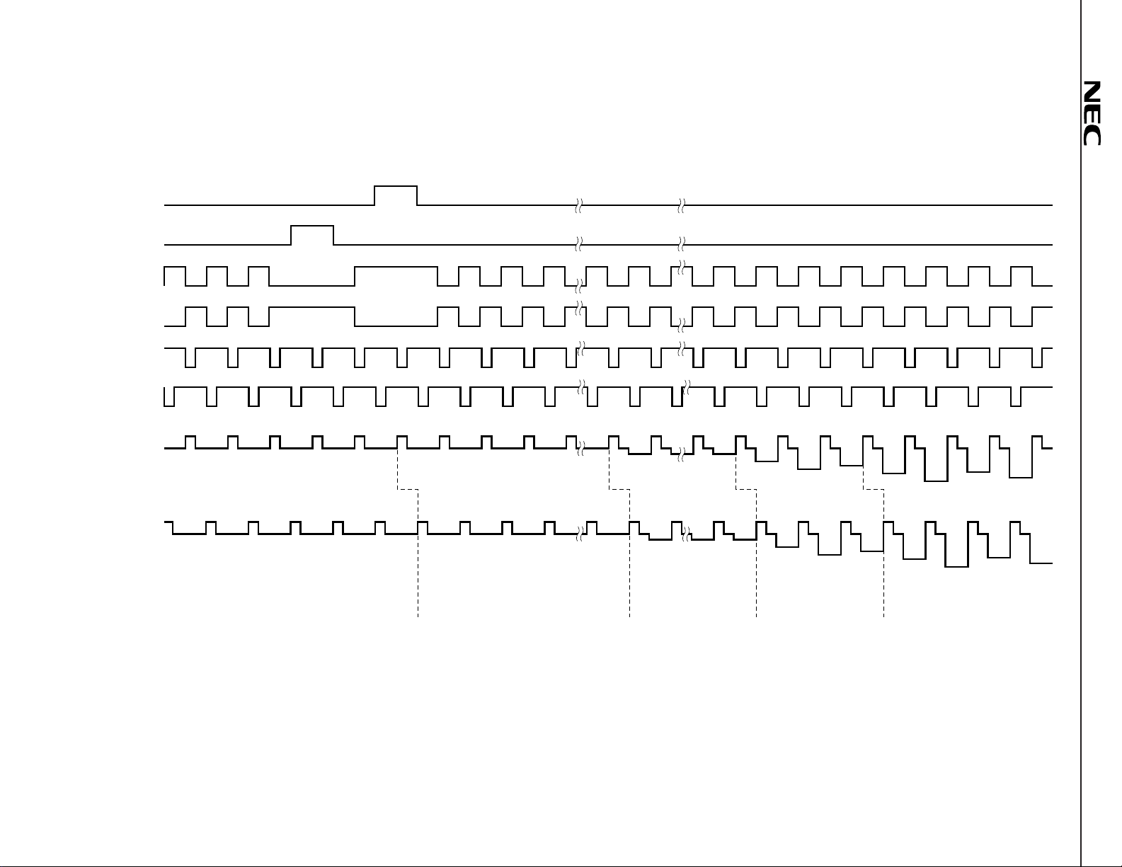
TIMING CHART 1
φ
φ
TG1, TG3
φ
φ
φ
φ
1A1 to 1A4, 1L
φ
2A1 to 2A4, 2L
φ
R1B
φ
R2B
V
OUT
1, 3, 5
OUT
2, 4, 6
V
TG2
φ
φ
R, B
G
0 1 2 3 13 60 61 62 63 64 65 66
D0 D2 D4 D8 D26 D122 D126 S1 S3 S5
D1 D3 D5 D25 D27 D123 D127 S2 S4 S6
Vacant transfer (26 bits) Optical black (96 bits) Invalid photocell (6 bits)
Valid photocell (5000 bits)
Caution Pins 18 (
And also pins 17 (
φ
1A1) and 15 (
φ
φ
1A2), 11 (
2A1) and 14 (
φ
1A3) and 8 (φ1A4) are each connected inside of the device, so do not input different timings to them.
φ
2A2), 12 (
φ
2A3) and 9 (
φ
2A4) are each connected inside of the device, so do not input different timings to them
µ
PD3725A
(refer to BLOCK DIAGRAM).
7
Page 8

8
TIMING CHART 2
φ
φ
TG1, TG3
φ
TG2
φ
φ
1A1 to 1A4, 1L
φ
φ
2A1 to 2A4, 2L
φ
R1B
φ
R2B
VOUT1, 3, 5
VOUT2, 4, 6
φ
φ
D132D130D128S4999S4997
S4996 S4998 S5000 D129 D131 D133
Invalid photocell (6 bits)
µ
PD3725A
Page 9

µ
PD3725A
TIMING CHART 3 (Usual speed drive f
t
10
t
1
φ
φ
1L, 1A1 to 1A4
φ
φ
2L, 2A1 to 2A4
φ
φ
φ
R2B
φ
R1B
10%
90%
t
2
t
t
3
5
t
4
φ
R1B, fφR2B = 1 to 5 MHz)
t
11
t
6
12
t
t13t14t
t
d
t
16
15
OUT
2, 4, 6
V
OUT
1, 3, 5
V
TIMING CHART 4
φ
2L, 2A1 to 2A4
φ
1L, 1A1 to 1A4
φ
φ
φ
φ
φ
TG2
t
d
90%
7t8
t
90%
V
OS
10%
V
OS
10%
t
9
t8t
7
t17t
18
t
19
t18t
17
φ
φ
TG1, TG3
9
Page 10

Recommended Timing
(Unit: ns)
Symbol MIN. TYP. MAX.
t1, t11 010–
t2, t12 050–
t3, t5, t13, t15 05–
t4, t14 20 50 –
t6, t16 20 50 –
t7, t17 20 50 –
t8, t18 050–
t9, t19 1000 2000 –
t10 100 500 –
φ
1A, φ2A cross points
φ
1A, 2A cross points
φφ
φ
1L, φ2A cross points
1L, 2A cross points
φ
µ
PD3725A
φ
1A
2 V or more
0.5 V or more
φ
2A
φ
1A, φ2L cross points
1A, 2L cross points
φ
φ
φ
1A
φ
2L
2 V or more
2 V or more
Remark 1. Adjust input resistance of each pin for cross points (
φ
1A: φ1A1 to φ1A4
2.
φ
2A: φ2A1 to φ2A4
φ
2A
2 V or more
φ
1L
φ
1A, φ2A), (φ1L, φ2A) and (φ1A, φ2L)
0.5 V or more
10
Page 11

µ
PD3725A
TIMING CHART5 (High speed drive f
t
21
90%
φ
φ
1A1 to 1A4
φ
φ
2A1 to 2A4
φ
1L
φ
2L
10%
φ
R1B, fφR2B = 5 to 8 MHz)
t
30
t
t
27
26
t
31
t
t
37
36
t
32
t
34
t
35
φ
R2B
φ
R1B
t
33
t
22
t
t
23
24
t
25
t
d
90%
OUT
2, 4, 6
V
V
OS
10%
t
d
90%
V
OUT
1, 3, 5
V
OS
10%
11
Page 12

µ
PD3725A
Recommended Timing (High speed drive f
Symbol MIN. TYP. MAX.
t21, t31 010—
t22, t32 030—
t23, t25, t33, t35 05—
t24, t34 20 t30/2 —
t26, t36 10 20 —
t27, t37 010—
t30 60 100 —
Caution When driving µPD3725A according to timing shown in TIMING CHART 3 at high speed, period
of signal output is shorten, therefore data may not be sampled normally.
To sample data normally, drive
extend the period of signal output, falling edge of last gate shift register clock φ1L, φ2L should
be earlier than that of shift register clock φ1A, φ2A.
When making the falling edge of
φ
R1B, φR2B. To avoid the effection of this noise, the falling edge of φR1B, φR2B should be set
earlier.
Driving at high speed, drive capability is necessary to be powered up. So design the peripheral
circuit referring to peripheral circuit example 2.
φ
R1B, fφR2B = 5 to 8 MHz)
(Unit: ns)
µ
PD3725A according to timing shown in TIMING CHART 5. To
φ
1L, φ2L early, output signal is effected by noise from reset clock
12
Page 13

µ
PD3725A
DEFINITIONS OF CHARACTERISTIC ITEMS
1. Saturation voltage: Vsat
Output signal voltage at which the response linearity is lost.
2. Saturation exposure: SE
Product of intensity of illumination (I
3. Photo response non-uniformity: PRNU
The peak/bottom ratio to the average output voltage of all the valid bits calculated by the following formula.
X) and storage time(s) when saturation of output voltage occurs.
VMAX. or VMIN.
PRNU(%)= x 100
n
1
∑ V
n
j=1
–1
j
n: Number of valid bits
j: Output voltage of each bit
V
n
1
Vj
S
n
j=1
Register Dark
DC level
V
MIN.
V
MAX.
4. Average dark signal: ADS
Output average voltage in light shielding
n
ADS(mV) = ∑ V
1
j
n
j=1
5. Dark signal non-uniformity: DSNU
The difference between peak or bottom output voltage in light shielding and ADS.
Register Dark
DC level
6. Output impedance: ZO
Output pin impedance viewed from outside.
7. Response: R
Output voltage divided by exposure (Ix•s).
Note that the response varies with a light source.
ADS
DSNU MIN.
DSNU MAX.
13
Page 14

8. Image Lag: IL
The rate between the last output voltage and the next one after read out the data of a line.
φ
TG
µ
PD3725A
Light
V
OUT
ON
V
IL = ×100 (%)
1
V
OUT
OUT
V
OFF
V
1
9. Register Imbalance: RI
The rate of the difference between the averages of the output voltage of Odd and Even bits, against the average
output voltage of all the valid bits.
n
2
2
(V
2j – 1
– V2j)
n
1
V
j
Σ
n
j=1
× 100 (%)
RI =
Σ
n
j=1
14
Page 15

STANDARD CHARACTERISTIC CURVES (TA = +25 °C)
DARK OUTPUT TEMPERATURE
CHARACTERISTICS
8
4
2
1
0.5
Relative Output Voltage
0.25
Relative Output Voltage
STORAGE TIME OUTPUT VOLTAGE
2
1
0.2
CHARACTERISTICS
µ
PD3725A
0.1
0 1020304050
Operating Ambient Temperature T
100
80
60
40
Response Ratio (%)
20
TOTAL SPECTRAL RESPONSE CHARACTERISTICS (without infrared cut filter)
B
A
(°C)
G
0.1
1510
Storage Time (ms)
R
G
B
0
400 500 600 700 800
Wavelength (nm)
15
Page 16

16
PERIPHERAL CIRCUIT EXAMPLE 1
B1
+12 V
+
µ
1
OUT3
V
V
OUT4
24
B4
0.1 F
_
µ
47 F/25 V
φ
φ
R2B
φ
TG1
2
B2
B3
10 Ω
µ
47 F/25 V
47 Ω
2
47 Ω
10 Ω
VOUT6
3
VOUT5
4
VOD
+
_
5
φ
R2B
2L
1A4
2A4
TG3
1A3
2A3
µ
PD3725AD
10
11
12
6
φ
7
GND
8
φ
9
φ
φ
φ
φ
VOUT1
VOUT2
GND
φ
R1B
φ
1L
φ
1A1
φ
2A1
φ
TG1
φ
1A2
φ
2A2
φ
TG2
23
22
21
20
19
18
17
16
15
14
13
B5
B6
47 Ω
10 Ω
10 Ω
47 Ω
φ
φ
φ
R1B
1
B1 to B6 EQUIVALENT CIRCUIT
CCD
V
OUT
TG2
100 Ω
100 Ω
+12 V
47 F/25 V
2 kΩ
µ
+
_
Remark Inverters:
µ
PD74HC04
µ
PD3725A
Page 17

PERIPHERAL CIRCUIT EXAMPLE 2 (For high speed drive)
B1
+12 V
+
µ
1
V
OUT
3
24
OUT
4
V
B4
0.1 F
_
µ
47 F/25 V
φ
φ
R2B
φ
TG1
2
OUT
6
B2
B3
10 Ω
µ
47 F/25 V
47 Ω
2
47 Ω
10 Ω
*
*
V
3
OUT
5
V
4
V
10
11
12
5
6
7
8
9
OD
φ
R2B
φ
2L
GND
φ
1A4
φ
2A4
φ
TG3
φ
1A3
φ
2A3
µ
PD3725AD
+
_
OUT
V
OUT
V
GND
φ
R1B
φ
φ
1A1
φ
2A1
φ
TG1
φ
1A2
φ
2A2
φ
TG2
1L
23
22
21
20
19
18
17
16
15
B5
B6
47 Ω
10 Ω
47 Ω
φ
φ
R1B
1
1
2
*
14
*
13
10 Ω
φ
TG2
17
Remarks 1. Inverters: 74AC04
2. For
inverter, use high speed inverter which has double driving capability of 74AC04
*
µ
PD3725A
Page 18

PACKAGE DIMENSIONS (Unit: mm)
CCD LINEAR IMAGE SENSOR 24PIN CERAMIC DIP (600 mil)
µ
PD3725A
(Unit : mm)
90.0±1.3
85.0±1.2
27.9
3.5±1.0
0.46±0.05
2.54
2.62
2 Connecting part
1 Pin 1 index
1.27±0.05
14.4
11.0±0.6
1bit
20.03±0.6
85.4±0.3
3 Connecting part
0.97±0.3
3.3±0.35
4.33
NOTE
1 pin 1 index and 2 , 3 connecting parts are
made of silver wax and plated with gold. As
they are electrically connected with GND, be
sure not to touch with other wirings on the
board.
6.4±0.3
15.1±0.3
15.24
(2.33)
2.0±0.3
Name Dimensions Refractive index
Glass cap 89.0 × 13.6 × 1.0 1.5
0.25±0.05
24D-1CCD-PKG-2
18
Page 19

µ
PD3725A
RECOMMENDED SOLDERING CONDITIONS
When soldering this product, it is highly recommended to observe the conditions as shown below. If other soldering
processes are used, or if the soldering is performed under different conditions, please make sure to consult with our
sales offices.
For more details, refer to our document “SEMICONDUCTOR DEVICE MOUNTING TECHNOLOGY MANUAL”
(C10535E).
Type of Through Hole Device
µ
PD3725AD : CCD linear image sensor 24-pin ceramic DIP (600 mil)
Process Conditions
Wave soldering (only to leads) Solder temperature: 260 °C or below,
Flow time: 10 seconds or less.
Partial heating method Pin temperature: 260 °C or below,
Heat time: 10 seconds or less (Per each lead).
Caution For through hole devices, the wave soldering process must be applied only to leads, and make
sure that the package body does not get jet soldered.
19
Page 20

[MEMO]
µ
PD3725A
20
Page 21

µ
NOTES FOR CMOS DEVICES
1 PRECAUTION AGAINST ESD FOR SEMICONDUCTORS
Note: Strong electric field, when exposed to a MOS device, can cause destruction
of the gate oxide and ultimately degrade the device operation. Steps must
be taken to stop generation of static electricity as much as possible, and
quickly dissipate it once, when it has occurred. Environmental control must
be adequate. When it is dry, humidifier should be used. It is recommended
to avoid using insulators that easily build static electricity. Semiconductor
devices must be stored and transported in an anti-static container, static
shielding bag or conductive material. All test and measurement tools
including work bench and floor should be grounded. The operator should
be grounded using wrist strap. Semiconductor devices must not be touched
with bare hands. Similar precautions need to be taken for PW boards with
semiconductor devices on it.
PD3725A
2 HANDLING OF UNUSED INPUT PINS FOR CMOS
Note: No connection for CMOS device inputs can be cause of malfunction. If no
connection is provided to the input pins, it is possible that an internal input
level may be generated due to noise, etc., hence causing malfunction. CMOS
device behave differently than Bipolar or NMOS devices. Input levels of
CMOS devices must be fixed high or low by using a pull-up or pull-down
circuitry. Each unused pin should be connected to VDD or GND with a
resistor, if it is considered to have a possibility of being an output pin. All
handling related to the unused pins must be judged device by device and
related specifications governing the devices.
3 STATUS BEFORE INITIALIZATION OF MOS DEVICES
Note: Power-on does not necessarily define initial status of MOS device. Produc-
tion process of MOS does not define the initial operation status of the device.
Immediately after the power source is turned ON, the devices with reset
function have not yet been initialized. Hence, power-on does not guarantee
out-pin levels, I/O settings or contents of registers. Device is not initialized
until the reset signal is received. Reset operation must be executed immediately after power-on for devices having reset function.
21
Page 22

µ
PD3725A
[MEMO]
The application circuits and their parameters are for references only and are not intended for use in actual design-in's.
No part of this document may be copied or reproduced in any form or by any means without the prior written
consent of NEC Corporation. NEC Corporation assumes no responsibility for any errors which may appear in this
document.
NEC Corporation does not assume any liability for infringement of patents, copyrights or other intellectual
property rights of third parties by or arising from use of a device described herein or any other liability arising
from use of such device. No license, either express, implied or otherwise, is granted under any patents,
copyrights or other intellectual property rights of NEC Corporation or others.
While NEC Corporation has been making continuous effort to enhance the reliability of its semiconductor devices,
the possibility of defects cannot be eliminated entirely. To minimize risks of damage or injury to persons or
property arising from a defect in an NEC semiconductor device, customer must incorporate sufficient safety
measures in its design, such as redundancy, fire-containment, and anti-failure features.
NEC devices are classified into the following three quality grades:
“Standard“, “Special“, and “Specific“. The Specific quality grade applies only to devices developed based on
a customer designated “quality assurance program“ for a specific application. The recommended applications
of a device depend on its quality grade, as indicated below. Customers must check the quality grade of each
device before using it in a particular application.
Standard: Computers, office equipment, communications equipment, test and measurement equipment,
audio and visual equipment, home electronic appliances, machine tools, personal electronic
equipment and industrial robots
Special: Transportation equipment (automobiles, trains, ships, etc.), traffic control systems, anti-disaster
systems, anti-crime systems, safety equipment and medical equipment (not specifically designed
for life support)
Specific: Aircrafts, aerospace equipment, submersible repeaters, nuclear reactor control systems, life
support systems or medical equipment for life support, etc.
The quality grade of NEC devices in “Standard“ unless otherwise specified in NEC's Data Sheets or Data Books.
If customers intend to use NEC devices for applications other than those specified for Standard quality grade,
they should contact NEC Sales Representative in advance.
Anti-radioactive design is not implemented in this product.
M4 94.11
 Loading...