

Page 1
DATA SHEET
MOS INTEGRATED CIRCUIT
µµµµ
PD31172
VRC4172
COMPANION CHIP FOR VR4121
DESCRIPTION
The µPD31172 (commercial name: VRC4172) is a companion chip designed for NEC’s µPD30121 microprocessor
(commercial name: VR4121).
The VRC4172 has the following functions available on chip: a USB host controller, an IEEE1284 parallel controller,
a 16550 serial controller, a PS/2 controller, general-purpose ports (GPIO), programmable chip select (PCS), and a
PWM controller (a duty modulated light pulse generation function for LCD backlighting).
The VRC4172 can be directly connected to the VR4121, allowing a reduction in the man-hours required for
development of a Windows™ CE system.
Detailed function descriptions are provided in the following user’s manual. Be sure to read it before
designing.
RC
•
V
4172 User’s Manual (U14386E)
FEATURES
• Directly connectable to VR4121
• On-chip USB host controller
• USB ports: 2
• Compliant with the USB OpenHCI specifications, release 1.0
• Communicates with USB device asynchronously with host CPU
• Full-speed (12 Mbps) and low-speed (1.5 Mbps) modes supported
• System clock: 48 MHz
• On-chip PS/2 controller
• On-chip IEEE1284 parallel controller
• On-chip 16550 serial controller
• General-purpose ports (GPIO): 24
• On-chip PWM controller
• Duty modulated light pulse generation function for LCD backlighting
• Internal maximum operating frequency: 48 MHz
• Power supply voltage: VDD = 3.3 V ± 0.3 V
• Package: 208-pin plastic FBGA
TM
TM
APPLICATIONS
Battery-driven portable information devices
•
Peripheral devices for PCs, etc.
•
The information in this document is subject to change without notice. Before using this document, please
confirm that this is the latest version.
Not all devices/types available in every country. Please check with local NEC representative for
availability and additional information.
Document No. U14388EJ2V0DS00 (2nd edition)
Date Published May 2000 N CP(K)
Printed in Japan
The mark shows major revised points.
Page 2
ORDERING INFORMATION
Part Number Package Internal Maximum Operating Frequency
PD31172F1-48-FN 208-pin plastic FBGA (15 × 15) 48 MHz
µ
PIN CONFIGURATION
208-pin plastic FBGA (15 × 15)
•
PD31172F1-48-FN
µ
Bottom View Top View
17
16
15
14
13
12
11
10
µµµµ
PD31172
9
8
7
6
5
4
3
2
1
ABCDEFGHJKLMNPRTU UTRPNMLKJHGFEDCBA
Index mark
2
Data Sheet U14388EJ2V0DS00
Page 3
µµµµ
PD31172
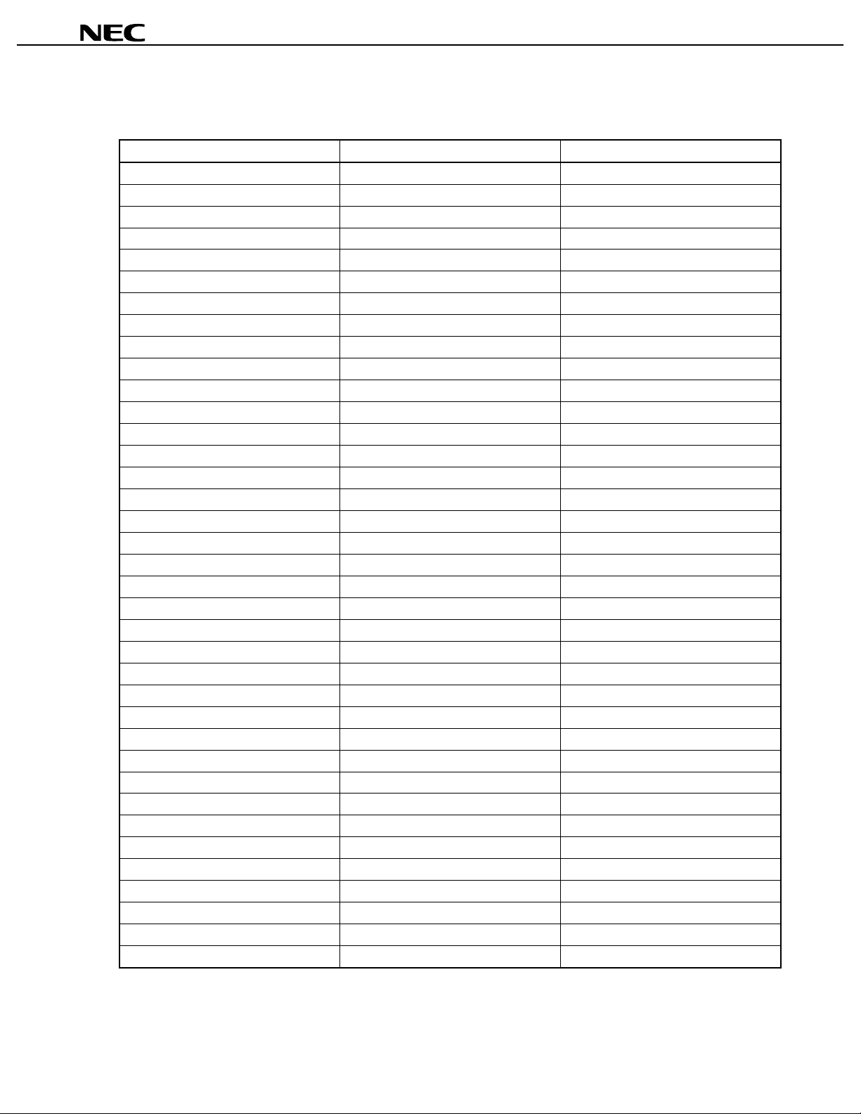
Symbol Name Symbol Name Symbol Name Symbol Name
A1 GND C2 GND E3 CD3 J15 GND
A2 AUTOFEED# C3 STROBE# E4 CD7 J16 UUCAS#
A3 PE C4 ACK# E14 GND J17 ROMCS3#
A4 INIT# C5 ERROR# E15 PPON1 K1 GPIO14
A5 IOCHRDY C6 AD6 E16 OCI2 K2 GPIO10
A6 AD19 C7 AD7 E17 USBRST# K3 GPIO7
A7 AD20 C8 AD8 F1 GPIO22 K4 GPIO3
A8 AD21 C9 V
DD
F2 GPIO18 K14 EXCS3#
A9 AD22 C10 AD9 F3 CD2 K15 EXCS0#
A10 AD23 C11 AD10 F4 CD6 K16 SCAS#
A11 AD24 C12 AD11 F14 SCLK K17 SRAS#
A12
A13
Reserved
Reserved
Note 1
Note 1
C13 LCDBAK F15 PPON2 L1 GPIO13
C14 SMI# F16 LCAS# L2 GPIO9
A14 DP1 C15 USBINT# F17 MRAS0# L3 GPIO6
A15 DN2 C16 GND G1 GPIO21 L4 GPIO2
A16 DP2 C17 RD# G2 GPIO17 L14 EXCS4#
A17 LCDRDY D1 GND G3 CD1 L15 EXCS1#
B1 PS2CLK D2 SELECTIN# G4 CD5 L16
B2 V
B3 V
DD
DD
D3 DIR1284 G14
D4 PS2INT G15
Reserved
Reserved
Note 1
Note 1
L17 GND
M1 GPIO12
Reserved (0)
B4 BUSY D5 SELECT G16 UCAS# M2 GPIO8
B5 GND D6 AD0 G17 MRAS1# M3 GPIO5
B6 AD12 D7 AD1 H1 GPIO20 M4 GPIO1
B7 AD13 D8 AD2 H2 GPIO16 M14 EXCS5#
B8 AD14 D9 GND H3 CD0 M15 EXCS2#
B9 AD15 D10 AD3 H4 CD4 M16
B10 AD16 D11 AD4 H14
Reserved
Note 1
M17 CKE
Reserved (0)
B11 AD17 D12 AD5 H15 ARBCLKSEL N1 RESET
B12 AD18 D13 V
DD
H16 ULCAS# N2 BUSRQ0#
B13 GND D14 IEN H17 ROMCS2# N3 GPIO4
B14 DN1 D15 WAKE J1 GPIO15 N4 GPIO0
B15 V
B16 GND D17 LCDCS# J3 V
DD
D16 OCI1 J2 GPIO11 N14 GND
DD
N15 DSR#
B17 WR# E1 GPIO23 J4 GND N16 RXD
C1 PS2DATA E2 GPIO19 J14 V
DD
N17 RI#
Note 2
Note 2
Notes 1.
Remark
Either leave pins A12, A13, G14, G15, and H14 open, or input 0 V.
Always input 0 V to pins L16 and M16.
2.
# indicates active low.
Data Sheet U14388EJ2V0DS00
3
Page 4
µµµµ
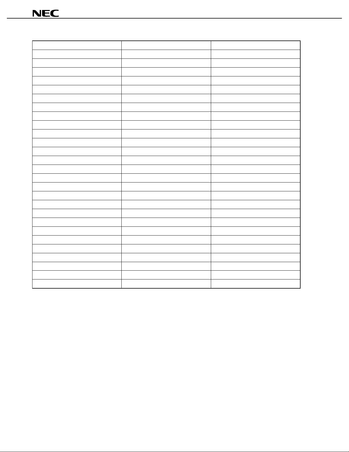
Symbol Name Symbol Name Symbol Name Symbol Name
P1 HOLDRQ# R1 HOLDAK# T1 BUSCLK U1 IOCS16#
P2 BUSAK0# R2 GND T2 GND U2 IRQ
P3 BUSRQ1# R3 BUSAK1# T3 V
P4 GND R4 DATA23 T4 V
P5 DATA31 R5 DATA22 T5 DATA15 U5 GND
P6 DATA30 R6 V
DD
T6 DATA14 U6 DATA7
P7 DATA29 R7 DATA21 T7 GND U7 DATA6
P8 DATA28 R8 DATA20 T8 DATA13 U8 DATA5
P9 V
DD
R9 GND T9 DATA12 U9 DATA4
P10 DATA27 R10 DATA19 T10 DATA11 U10 DATA3
P11 DATA26 R11 DATA18 T11 DATA10 U11 DATA2
P12 DATA25 R12 V
DD
T12 GND U12 DATA1
P13 DATA24 R13 DATA17 T13 DATA9 U13 DATA0
P14 CLKOUT48M R14 DATA16 T14 DATA8 U14 GND
P15 DCD# R15 CTS# T15 V
P16 TXD R16 GND T16 V
P17 INTRP R17 XOUT48M T17 XIN48M U17 GND
DD
DD
DD
DD
U3 IOR#
U4 IOW#
U15 DTR#
U16 RTS#
PD31172
Remark
# indicates active low.
4
Data Sheet U14388EJ2V0DS00
Page 5

µµµµ
PD31172
PIN IDENTIFICATION
ACK#: Acknowledge MRAS (0:1)#: DRAM Row Address Strobe
AD (0:24): Address Bus OCI (1:2): Over Current Interrupt
ARBCLKSEL: Arbitration Clock Select PE: Paper End
AUTOFEED#: Autofeed PPON (1:2): Port Power ON
BUSAK (0:1)#: Bus Acknowledge PS2CLK: PS2 Clock
BUSCLK: System Bus Clock PS2DATA: PS2 Data
BUSRQ (0:1)#: Bus Request PS2INT: PS2 Interrupt
BUSY: Busy RD#: Read
CD (0:7): Centronics Data RESET: Reset
CKE: Clock Enable RI#: Ring Indicator
CLKOUT48M: Clock Out of 48 MHz ROMCS (2:3)#: ROM Chip Select
CTS#: Clear to Send RTS#: Request to Send
DATA (0:31): Data Bus RXD: Receive Data
DCD#: Data Carrier Detect Column Address Strobe for
DIR1284: Direction of 1284
DN (1:2): USB D
DP (1:2): USB D+ SELECT: Select
DSR#: Data Set Ready SELECTIN#: Select in
DTR#: Data Terminal Ready SMI#: USB System Interrupt
ERROR#: Error Row Address Strobe for
EXCS (0:5)#: External CS
GND: Ground STROBE#: Strobe
GPIO (0:23): General Purpose I/O TXD: Transmit Data
HOLDAK#: Hold Acknowledge UCAS#: Upper Column Address Strobe
HOLDRQ#: Hold Request Lower Byte of Upper Column
IEN: USB Input Enable
INIT# Initialize USBINT#: USB Interrupt
INTRP: Interrupt USBRST#: USB Reset
IOCHRDY: I/O Channel Ready Upper Byte of Upper Column
IOCS16#: IO Chip Select 16
IOR#: I/O Read VDD: Power Supply Voltage
IOW#: I/O Write WAKE: Wake Up Interrupt
IRQ: I/O Request WR#: Write
LCAS#: Lower Column Address Strobe XIN48M: Clock In of 48 MHz
LCDBAK: LCD Back Light XOUT48M: Clock Out of 48 MHz
LCDCS#: LCD Chip Sel ect
LCDRDY: LCD Ready
−
SCAS#:
SDRAM
SCLK: SDRAM Clock
SRAS#:
SDRAM
ULCAS#:
Address Strobe
UUCAS#:
Address Strobe
Remark
# indicates active low.
Data Sheet U14388EJ2V0DS00
5
Page 6
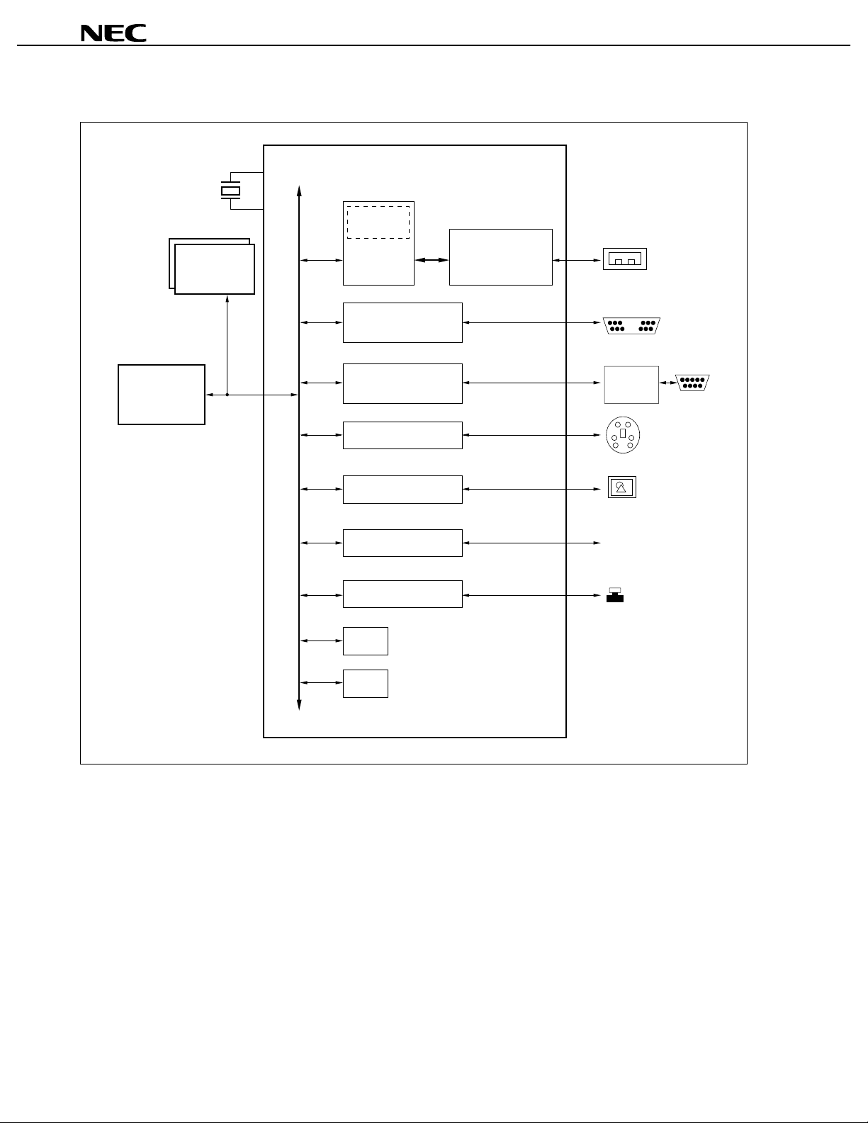
INTERNAL BLOCK DIAGRAM AND EXTERNAL BLOCK CONNECTION EXAMPLE
V
RC
4172
48 MHz
DRAM
controller
USB host
Internal PCI bus
controller
(OpenHCI 1.0)
SDRAM
PCI bus
controller
2 ports
µµµµ
PD31172
V
R
4121
System bus
IEEE1284
parallel controller
16550
serial controller
PS/2 controller
PWM controller
PCS (6 bits)
GPIO (24 bits)
PMU
ICU
. . . .
. . . .
RS-232-C
driver
LCD backlight
6
Data Sheet U14388EJ2V0DS00
Page 7

µµµµ
PD31172
CONTENTS
1. PIN FUNCTIONS................................................................................................................................... 8
1.1 Pin Function List .......................................................................................................................................8
1.2 Special Status Pins .................................................................................................................................11
1.3 External Processing of Pins and Drive Capacity.................................................................................. 13
1.4 Recommended Connection of Unused Pins......................................................................................... 15
2. ELECTRICAL SPECIFICATIONS...................................................................................................... 16
3. PACKAGE DRAWING....................................................................................................................... 38
4. RECOMMENDED SOLDERING CONDITIONS................................................................................ 39
Data Sheet U14388EJ2V0DS00
7
Page 8
µµµµ
1. PIN FUNCTIONS
1.1
Pin Function List
(1) System bus interface signals
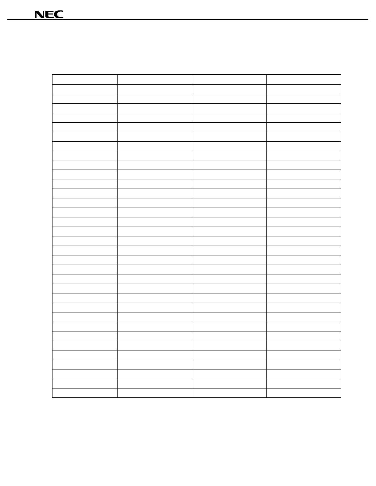
Signal Name I/O Function
SCLK I/O This i s the SDRAM operating clock .
AD (0:24) I/O These form a 25-bit address bus.
DATA (0:31) I/O These form a 32-bit data bus.
LCDCS# Input This is the LCD chip sel ec t signal. This signal becomes active when the VR4121 accesses the
LCD using the AD or data bus.
RD# I/O
WR# I/O
LCDRDY Output T hi s is the LCD ready signal. Thi s signal becomes acti ve when a state is entered whereby t he
ROMCS (2:3)# I/O This is an SDRAM chip select signal.
CKE I/O This is t he SDRAM clock enable si gnal .
UUCAS# I/O Thi s is an SDRAM DQM signal. This signal controls the I/O buffers for the DATA (24:31) pins.
ULCAS# I/O This is an SDRAM DQM signal. This signal controls the I/ O buf fers for the DATA (16:23) pins.
MRAS (0:1)# I/ O This is an SDRAM chip select s i gnal .
UCAS# I/O This is an S DRA M DQM signal. This signal controls the I/O buffers for the DATA (8:15) pins.
LCAS# I/O This is an SDRAM DQM si gnal . This signal controls t he I/O buffers for the DATA (0:7) pins.
IOR# Input This is the system bus I/O read signal. This signal becomes active when any resource except
IOW# Input
RESET Input This is the system bus reset signal.
IOCS16# Output Thi s is the dynamic bus-s i zing request signal.
IOCHRDY Output T hi s is the system bus ready signal.
HOLDRQ# Output This is the system bus access right request signal.
HOLDAK# Input This is the system bus access enable signal.
SRAS# I/O This is the SDRAM RAS signal.
SCAS# I/O This is the SDRAM CAS signal.
BUSRQ (0:1)# Input This is a signal input f rom the external bus master requesting access to the system bus.
BUSAK (0:1)# Output This is a signal out put t o t he external bus master permitting access t o t he system bus.
INTRP Output This is an interrupt request signal from the 16550 serial controller or the I EEE1284 parallel
IRQ Output This is an interrupt request signal from the general-purpose ports (GPIO (0:23)) or the
USBINT# Output This is an interrupt request signal f rom the USB host controller.
PS2INT Output This is an interrupt request signal from the PS/2 c ont rol l er.
BUSCLK Input This is the system bus clock.
ARBCLKSEL Input This is a clock select signal for arbitrating the system bus (controls the HOLDRQ# signal)
Output: This signal becomes ac tive when the VRC4172 accesses SDRAM.
•
R
Input: This signal becomes ac tive when the V
•
host bridge.
Output: This signal becomes ac tive when the VRC4172 writes data to SDRAM.
•
Input: This signal becomes active when the V
•
bridge.
RC
V
4172 can acknowledge an access t o the LCD area from the VR4121.
the USB inside the V
This is the system bus I/O write signal. This signal becomes active when
the USB inside the V
controller.
IEEE1284 parallel controll er.
(1: Internal clock us ed, 0: BUSCLK used)
RC
4172 is accessed.
RC
4172 is accessed.
4121 reads data from the VRC4172’s PCI
R
4121 writes data to the VRC4172’s PCI host
any
resource except
PD31172
8
Data Sheet U14388EJ2V0DS00
Page 9
µµµµ
PD31172
(2) USB Interface Signals
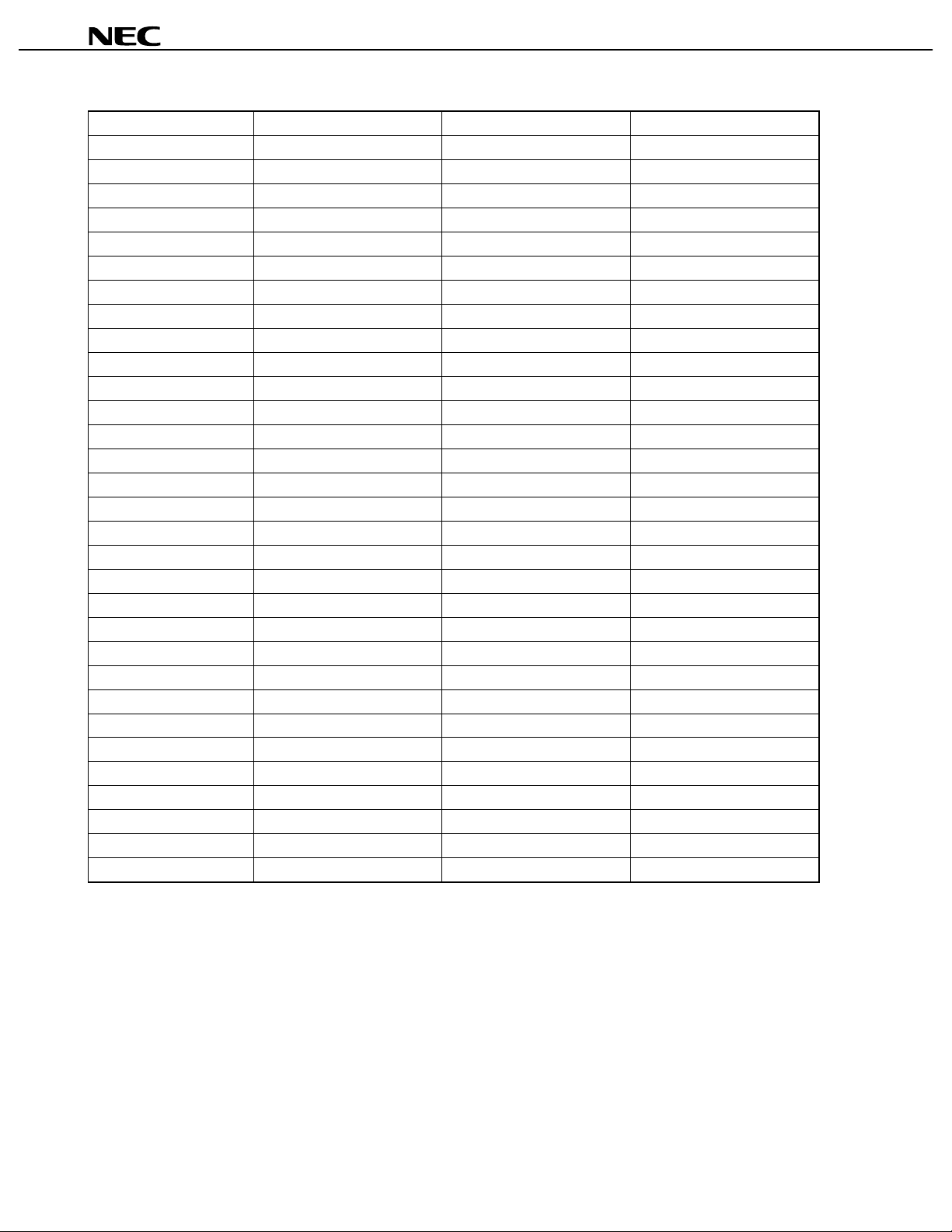
Signal Name I/O Function
DP (1:2) I /O This i s the positive data s i gnal .
DN (1:2) I/O This is the negativ e data signal.
PPON (1:2) Output This is the USB route-hub-port power supply control si gnal .
OCI (1:2) Input This is the US B route-hub-port over-current status signal. Make this s i gnal active when the
current flowing through the Vbus l i ne of the USB exceeds the ref erence value.
IEN Input This is the USB buf fer input enable signal. Make t hi s signal active when the i nput signal to the
USB port is validated.
WAKE Output This is a wakeup interrupt request signal .
SMI# Output This is a system interrupt request signal.
USBRST# Input This is the reset signal for the USB cloc k.
(3) IEEE1284 Interface Signals
Signal Name I/O Function
CD (0:7) I/O These are data signals
STROBE# I/O This is the data s t robe signal.
ACK# I/O This i s the acknowledge signal.
BUSY I/O This is the busy signal.
PE I/O Thi s is the paper-end signal.
SELECT I/O This is t he s el ec t signal.
AUTOFEED# I/O This is the aut of eed signal.
SLECTIN# I/O This is t he s el ect input signal.
ERROR# I/O This is the fault signal.
INIT# I / O This is the initialization signal.
DIR1284 Output This signal outputs the transfer direction status.
(4) RS-232-C Interface Signals
Signal Name I/O Function
RXD Input This is the receive data signal.
CTS# I nput This is the transmit enable signal.
DSR# Input This is the data set ready s i gnal .
TXD Output Thi s i s the transmit data signal.
RTS# Output This is the transmit request signal.
DTR# Output This is the t erm i nal equi pm ent ready signal.
DCD# Input This is the carrier detection signal.
RI# Input This is the c al l di s pl ay signal.
Data Sheet U14388EJ2V0DS00
9
Page 10
(5) PS/2 Interface Signals
Signal Name I/O Function
PS2CLK I/O This is t he PS/2 clock signal .
PS2DATA I/O This is the PS/2 data s i gnal .
(6) General-Purpose Port Signals
Signal Name I/O Function
GPIO (0:23) I/O Thes e are general -purpose I/O signals.
(7) General-Purpose Chip Select Signals
Signal Name I/O Function
EXCS (0:5)# Output These are general-purpose chip select signal s.
(8) LCD Interface Signals
Signal Name I/O Function
LCDBAK Output These are signals f or controlling the LCD backlighting.
µµµµ
PD31172
(9) Clock Signals
Signal Name I/O Function
XIN48M Input This is the 48 MHz oscillator input pin. Connect to one side of a cryst al res onator.
XOUT48M Output This is the 48 MHz oscillator output pin. Connect to the ot her side of the crystal resonat or.
CLKOUT48M Output This is the 48 MHz cloc k output for the FIR of the VR4121.
10
Data Sheet U14388EJ2V0DS00
Page 11
µµµµ
1.2 Special Status Pins
Signal Name After Res et When HOLDAK# = 1
SCLK Hi-Z Hi-Z
AD (0:24) Hi-Z Hi-Z
DATA (0:31) Hi-Z Hi-Z
LCDCS#
RD# Hi-Z Hi-Z
WR# Hi-Z Hi-Z
LCDRDY Hi-Z Hi-Z
ROMCS (2:3)# Hi-Z Hi-Z
CKE Hi-Z Hi-Z
UUCAS# Hi-Z Hi-Z
ULCAS# Hi-Z Hi-Z
MRAS (0:1)# Hi-Z Hi-Z
UCAS# Hi-Z Hi-Z
LCAS# Hi-Z Hi-Z
IOR#
IOW#
RESET
IOCS16# Hi-Z Hi-Z
IOCHRDY Hi-Z Hi-Z
HOLDRQ# 1 1
HOLDAK#
SRAS# Hi-Z Hi-Z
SCAS# Hi-Z Hi-Z
BUSRQ (0:1)#
BUSAK (0:1)# 1 Normal operation
INTRP 0 Normal operation
IRQ 0 Normal operation
USBINT# 1 Normal operation
PS2INT 0 Normal operation
BUSCLK
ARBCLKSEL
DP (1:2) 1 Normal operation
DN (1:2) 0 Normal operation
PPON (1:2) 0 Normal operation
OCI (1:2)
IEN
WAKE 0 Normal operati on
−−
−−
−−
−−
−−
−−
−−
−−
−−
−−
PD31172
(1/2)
Remark
0: Low level, 1: High level, Hi-Z: High impedance
Data Sheet U14388EJ2V0DS00
11
Page 12
Signal Name After Res et When HOLDAK# = 1
SMI# 1 Normal operation
USBRST#
CD (0:7) Hi-Z Normal operation
STROBE# Hi-Z Normal operation
ACK# Hi-Z Normal operation
BUSY Hi-Z Normal operation
PE Hi-Z Normal operation
SELECT Hi-Z Normal operation
AUTOFEED# Hi-Z Normal operation
SELECTIN# Hi-Z Normal operation
ERROR# Hi-Z Normal operation
INIT# Hi-Z Normal operation
DIR1284 0 Normal operation
RXD
CTS#
DSR#
TXD 1 Normal operation
RTS# 1 Normal operati on
DTR# 1 Normal operation
DCD#
RI#
PS2CLK 0 Normal operation
PS2DATA Hi-Z Normal operation
GPIO (0:23) Hi-Z Normal operation
EXCS (0:5)# 1 Normal operation
LCDBAK 0 Normal operation
CLKOUT48M 1 Normal operation
−−
−−
−−
−−
−−
−−
µµµµ
PD31172
(2/2)
Remark
12
0: Low level, 1: High level, Hi-Z: High impedance
Data Sheet U14388EJ2V0DS00
Page 13
1.3 External Processing of Pins and Drive Capacity
µµµµ
PD31172
When using the V
RC
4172, process the pins externally, as shown in the table below.
Signal Name External Processing Drive Capacity Tolerance
SCLK
AD (0:24)
DATA (0:31)
−
−
−
LCDCS# Pull up
RD#
WR#
Pull up
Pull up
Note 1
Note 1
80 pF 3 V
80 pF 3 V
80 pF 3 V
−
3 V
80 pF 3 V
80 pF 3 V
LCDRDY Pull up 40 pF 3 V
ROMCS (2:3)# Pull up 80 pF 3 V
CKE Pull down 80 pF 3 V
Note 1
UUCAS#
ULCAS#
MRAS (0:1)#
UCAS#
LCAS#
IOR#
IOW#
RESET
Pull up
Pull up
Pull up
Pull up
Pull up
Pull up
Pull up
Note 1
Note 1
Note 1
Note 1
Note 1
Note 1
80 pF 3 V
80 pF 3 V
80 pF 3 V
80 pF 3 V
80 pF 3 V
−
−
−−
3 V
3 V
3 V
IOCS16# Pull up 40 pF 3 V
IOCHRDY Pull up 40 pF 3 V
HOLDRQ#
−
HOLDAK# Pull up
SRAS#
SCAS#
BUSRQ (0:1)#
BUSAK (0:1)#
INTRP
IRQ
USBINT#
PS2INT
BUSCLK
ARBCLKSEL
DP (1:2)
DN (1:2)
Pull up
Pull up
−−
−
−
−
−
−
−−
−−
−
−
Note 1
Note 1
40 pF 3 V
−
80 pF 3 V
80 pF 3 V
40 pF 3 V
40 pF 3 V
40 pF 3 V
40 pF 3 V
40 pF 3 V
Note 2
Note 2
3 V
3 V
3 V
3 V
5 V
5 V
(1/2)
Notes 1.
Remark
R
The same specification has been made for these pins in the V
4121. If these pins have been processed in
the VR4121, there is no need to perform this processing in the VRC4172.
In full-speed mode: 50 pF, In low-speed mode: 350 pF
2.
There is no need to perform external processing if no particular external processing has been specified (−).
Data Sheet U14388EJ2V0DS00
13
Page 14
Signal Name External Processing Drive Capacity Tolerance
PPON (1:2)
OCI (1:2)
IEN
WAKE
SMI#
USBRST#
CD (0:7)
STROBE# Pull up 40 pF 3 V
ACK# Pull up 40 pF 3 V
BUSY Pul l down 40 pF 3 V
PE Pull down 40 pF 3 V
SELECT Pull down 40 pF 3 V
AUTOFEED# Pull up 40 pF 3 V
SELECTIN# Pull up 40 pF 3 V
ERROR# Pul l up 40 pF 3 V
INIT# Pull up 40 pF 3 V
DIR1284
RXD
CTS#
DSR#
TXD
RTS#
DTR#
DCD#
RI#
PS2CLK P ul l up 40 pF 5 V
PS2DATA Pull up 40 pF 5 V
GPIO (0:23) Pull up/pull down 40 pF 3 V
EXCS (0:5)#
LCDBAK
CLKOUT48M
−
−−
−−
−
−
−−
−
−
−−
−−
−−
−
−
−
−−
−−
−
−
−
40 pF 3 V
3 V
3 V
40 pF 3 V
40 pF 3 V
3 V
40 pF 3 V
40 pF 3 V
3 V
3 V
3 V
40 pF 3 V
40 pF 3 V
40 pF 3 V
3 V
3 V
40 pF 3 V
40 pF 3 V
40 pF 3 V
µµµµ
PD31172
(2/2)
Remark
14
There is no need to perform external processing if no particular external processing has been specified (−).
Data Sheet U14388EJ2V0DS00
Page 15

µµµµ
PD31172
1.4 Recommended Connection of Unused Pins
Connect unused pins as shown in the table below.
Signal Name Recommended Connection Signal Nam e Recommended Connection
SCLK Pul l up PPON (1:2) Leave open
AD (0:24)
DATA (0:31)
LCDCS# Pull up WAKE Leave open
RD# Pull up SMI# Leave open
WR# Pull up USBRST# Pull down
LCDRDY Leave open CD (0:7) Pull down
ROMCS (2:3)# Pull up STROBE# Pull up
CKE Pull down ACK# Pull up
UUCAS# Pull up BUSY Pull down
ULCAS# Pull up PE Pull down
MRAS (0:1)# Pull up SELECT Pull down
UCAS# Pull up AUTOFEED# Pull up
LCAS# Pull up SELECTIN# Pull up
IOR#
IOW#
RESET
IOCS16#
IOCHRDY
HOLDRQ# Leave open DSR# Pull up
HOLDAK# Pull up TXD Leave open
SRAS# Pull up RTS# Leave open
SCAS# Pull up DTR# Leave open
BUSRQ (0:1)# Pull up DCD# Pull up
BUSAK (0:1)# Leave open RI# Pull up
INTRP Leave open PS2CLK Pul l up
IRQ Leave open PS2DATA Pull up
USBINT# Leave open GPIO (0: 23) Pull down
PS2INT Leave open EXCS (0:5)# Leave open
BUSCLK Pull up LCDBAK Leave open
ARBCLKSEL Pull down XIN48M Pull up
DP (1:2) Pull down XOUT48M Leave open
DN (1:2) Pull down CLKOUT48M Leave open
−
−
−
−
−
−
−
OCI (1:2) Pull down
IEN Pull down
ERROR# Pull up
INIT# Pull up
DIR1284 Leave open
RXD Pull down
CTS# Pull up
Remark
Pins with no particular specification (−) cannot be left unconnected.
Data Sheet U14388EJ2V0DS00
15
Page 16

2. ELECTRICAL SPECIFICATIONS
µµµµ
PD31172
Absolute Maximum Ratings (TA = 25
Parameter Symbol Conditions Ratings Unit
Power supply voltage V
Operating ambient temperature T
Storage temperature T
C)
°°°°
DD
I
VI < VDD + 0.5 V
VI < VDD + 3.0 V, DP (2:1), DN (2:1), PS2CLK,
PS2DATA pins
O
VO < VDD + 0.5 V
VO < VDD + 3.0 V, DP (2:1), DN (2:1), PS2CLK,
PS2DATA pins
A
stg
Cautions 1. Do not simultaneously short multiple outputs.
2. Product quality may suffer if the absolute maximum rating is exceeded even momentarily for any
parameter. That is, the absolute maximum ratings are rated values at which the product is on
the verge of suffering physical damage, and therefore the product must be used under
conditions that ensure that the absolute maximum ratings are not exceeded. The ratings and
conditions displayed in DC Characteristics and AC Characteristics in this section indicate the
ranges in which normal operation and product quality can be guaranteed.
0.5 to +4.6 V
−
0.5 to +4.6 VInput voltage V
−
0.5 to +6.6 V
−
0.5 to +4.6 VOutput voltage V
−
0.5 to +6.6 V
−
40 to +85
−
65 to +150
−
C
°
C
°
Capacitance (TA = 25
Parameter Symbol Conditions MIN. MAX. Unit
Input capacitance C
Output capacitance C
Output capacitance
Applicable to DP (2:1), DN (2:1), PS2CLK, and PS2DATA pins.
Note
C, VDD = 0 V)
°°°°
Note
I
f = 1 MHz
Unmeasured pins returned to 0 V.
O1
O2
C
8pF
8pF
12 pF
16
Data Sheet U14388EJ2V0DS00
Page 17

µµµµ
PD31172
DC Characteristics (TA =
40 to +85
−−−−
°°°°
(1) Pins except for DP (2:1), DN (2:1)
Parameter Symbol Conditions MIN. MAX. Unit
Output voltage, high V
Output voltage, low V
Output voltage, high
Output voltage, low
Output voltage, high
Output voltage, low
Note 1
Note 1
Note 2
Note 2
Input voltage, high V
Input voltage, high
Note 2
Input voltage, low V
Power supply current I
Input leakage current I
Input leakage current, high I
Output leakage current I
OH1IOH
OL1IOL
OH2IOH
V
OL2IOL
V
OH3IOH
V
OL3IOL
V
IH1
IH2
V
IL
DD
LI
VI = VDD, GND
LIH
VI = VDD, ARBCLKSEL pin 141
LO
VO = VDD, GND
C, VDD = 3.3
0.3 V)
±±±±
= −6 mA 2.4 V
= 6 mA 0.4 V
= −9 mA 2.4 V
= 9 mA 0.4 V
= −3 mA 2.4 V
= 3 mA 0.4 V
2.0 V
DD
2.0 5.5 V
00.8V
300 mA
10
±
10
±
V
A
µ
A
µ
A
µ
Notes 1.
Applicable to SCLK, AD (24:0), DATA (31:0), RD#, WR#, ROMCS (3:2)#, CKE#, UUCAS#, ULCAS#, MRAS
(1:0)#, UCAS#, LCAS#, SRAS#, and SCAS# pins.
Applicable to PS2CLK and PS2DATA pins.
2.
(2) DP (2:1), DN (2:1) pins
Parameter Symbol Conditions MIN. MAX. Unit
Output voltage, high V
Output voltage, low V
Differential input sens i tivity V
Differential common mode
range
Input voltage, high V
Input voltage, low V
Remark
Refer to the USB specification, revision 1.0, for details.
OH
RL = 15 kΩ (connected to GND) 2.8 3.6 V
OL
RL = 1.5 kΩ (connected to VDD)0.3V
DI
CMVDI
V
IH_USB
IL_USB
< 200 mV 0.8 2.5 V
0.2 V
2.0 V
0.8 V
Data Sheet U14388EJ2V0DS00
17
Page 18

µµµµ
PD31172
AC Characteristics (TA =
AC test input waveform
V
DD
0 V
AC test output test points
V
DD
0 V
40 to +85
−−−−
C, VDD = 3.3
°°°°
1.4 VAll output pins
1.4 VAll output pins
0.3 V)
±±±±
1.4 VTest points
1.4 VTest points
18
Data Sheet U14388EJ2V0DS00
Page 19

µµµµ
PD31172
Load Conditions
(a) SCLK, AD (0:24), DATA (0:31), RD#, WR#, ROMCS (2:3 )#, CLK#, UUCAS#, ULCAS#, ULCAS#, MRAS
(0:1)#, UCAS#, LCAS#, SRAS#, SCAS#
SCLK, AD (0:24), DATA (0:31),
RD#, WR#, ROMCS (2:3)#, CLK#,
UUCAS#, ULCAS#, MRAS (0:1)#,
UCAS#, LCAS#, SRAS#, SCAS#
DUT
CL = 80 pF
(b) DP (1:2), DN (1:2)
DP (1:2), DN (1:2)
(c) Other output pins
Output pins (except for (a) and (b) above)
DUT
DUT
In full-speed mode: CL = 50 pF
In low-speed mode: C
L
= 350 pF
CL = 40 pF
Data Sheet U14388EJ2V0DS00
19
Page 20

(1) Clock parameters
Parameter Symbol Conditions MIN. TYP. MAX. Unit
XIN48M clock frequenc y f
(2) Reset parameters
Parameter Symbol Conditions MIN. MAX. Unit
RESET signal high-level width t
USBRST# signal low-level width t
(3) SDRAM interface parameters
Parameter Symbol Conditions MIN. MAX. Unit
SCLK cycle t
SCLK high-level width t
SCLK low-level width t
Data output hold time t
Data output delay time t
Data input setup time t
Data input hold time t
CLK
RST
USBRST
SCLK
SCLKH
SCLKL
SDM
SDO
SDS
SDH
µµµµ
PD31172
48.0 50.0 MHz
30 ns
30 ns
20.8 ns
8ns
8ns
2ns
15 ns
9.5 ns
2ns
SCLK (I/O)
AD (24:0), WR#,
ROMCS (3:2)#,
UUCAS#, ULCAS#,
UCAS#, LCAS#,
MRAS (1:0)#, SRAS#,
SCAS#, CKE (I/O)
DATA (31:0) (output)
DATA (31:0) (input)
t
SCLKL
t
SDStSDH
t
SDM
t
SCLKH
t
SDO
Hi-Z Hi-Z
t
SCLK
20
Data Sheet U14388EJ2V0DS00
Page 21

(4) System bus interface parameters
(a) Access to I/O area
Parameter Symbol Conditions MIN. MAX. Unit
Command signal low-level wi dth t
Address setup time (t o command signal) t
Address hold time (from c ommand signal) t
IOCS16# valid delay tim e t
IOCS16# floating delay ti m e t
Data output hold time t
Data output delay time t
Data input setup time t
Data input setup time
Data input hold time t
During 16550-compatible serial communication
Note
Note
CLCH
AVCL
CHAV
AVCV
AVCZ
DM
DO
DS1
DS2
t
DH
µµµµ
PD31172
130 ns
10 ns
10 ns
12 ns
10 ns
625ns
30 ns
10 ns
10 ns
10 ns
AD (24:0)
(input)
IOR#/IOW#
(input)
t
AVCV
IOCS16#
(output)
DATA (31:0)
(input)
DATA (31:0)
(input)
Note
DATA (31:0)
(output)
During 16550-compatible serial communication
Note
Remark
The broken lines indicate high impedance
t
AVCL
t
DS2
t
t
CLCH
t
DS1tDH
t
DO
CHAV
t
AVCZ
t
DH
t
DM
Data Sheet U14388EJ2V0DS00
21
Page 22

(b) Access to LCD area
Parameter Symbol Conditions MIN. MAX. Unit
Command signal low-level wi dth t
Address setup time (t o command signal) t
Address hold time (from c ommand signal) t
LCDRDY valid delay tim e t
LCDRDY set delay time t
LCDRDY floating delay ti m e t
Data output hold time t
Data output delay time t
Data output valid time t
Data input setup time t
Data input hold time t
(i) When accessing the internal PCI bus
CLCH
AVCL
CHAV
AVRH
CLRL
AVRZ
DM
DO
DV
DS
DH
µµµµ
PD31172
90 ns
10 ns
10 ns
15 ns
12 ns
10 ns
625ns
30 ns
10 ns
10 ns
10 ns
Remark
AD (24:0)
(input)
LCDCS#
(input)
t
AVCL
RD#/WR#
(input)
t
AVRH
t
LCDRDY
(output)
t
DS
DATA (31:0)
(input)
DATA (31:0)
(output)
The broken lines indicate high impedance
CLRL
t
CLCH
t
CHAV
t
AVRZ
t
DH
t
t
DV
DM
22
Data Sheet U14388EJ2V0DS00
Page 23

(ii) When accessing the configuration register of the PCI host controller
AD (24:0)
(input)
LCDCS#
(input)
t
AVCL
RD#/WR#
(input)
t
CLCH
t
CHAV
µµµµ
PD31172
LCDRDY
(output)
DATA (31:0)
(input)
DATA (31:0)
(output)
Hi-Z
t
DS
t
DH
t
t
DO
DM
Hi-ZHi-Z
Data Sheet U14388EJ2V0DS00
23
Page 24

(5) GPIO parameters
Parameter Symbol Conditions MIN. MAX. Unit
GPIO (23:0) output delay ti m e t
GPIO (23:0) interrupt request generat i on time t
GPIO (23:0) interrupt request clear time t
(a) In output mode
IOW#
(input)
GPIO (23:0)
(output)
(b) In input mode
GIC
µµµµ
PD31172
GO
GI
30 ns
30 ns
35 ns
t
GO
GPIO (23:0)
(input)
IRQ (output)
(level trigger
interrupt)
IRQ (output)
(edge trigger
interrupt)
IOW# (input)
(edge interrupt
request clear)
t
t
GI
GI
t
GIC
24
Data Sheet U14388EJ2V0DS00
Page 25

(6) PCS (Programmable Chip Select) parameters
Parameter Symbol Conditions MIN. MAX. Unit
EXCS output delay tim e t
AD (24:0)
(I/O)
EXCS (5:0)#
(output)
EO
t
EO
(7) PWM (Pulse Width Modulation) parameters
Parameter Symbol Conditions MIN. MAX. Unit
LCDBAK output delay time t
LO
µµµµ
PD31172
30 ns
t
EO
SCLK
8 t
ns
IOW#
(input)
LCDBAK
Note
(output)
High level: enable, Low level: disable
Note
t
LO
Data Sheet U14388EJ2V0DS00
25
Page 26

(8) PS/2 parameters
Parameter Symbol Conditions MIN. MAX. Unit
PS2CLK clock high-l e vel width t
PS2CLK clock low-level width t
PS2CLK output delay tim e t
Transmission start t i m e t
Transmit data output delay time t
Receive data setup time t
Receive data hold time t
Receive disable setup ti me t
PSCH
PSCL
PSO
PSGO
PSDO
PSDS
PSDH
PSN
µµµµ
PD31172
3 T ns
3 T ns
T + 20 ns
20 ns
3 T + 20 ns
0ns
4 T ns
3 T ns
Remark
T = 125 ns (cycle of internal clock for controlling PS/2)
(a) Transmission
IOW#
(input)
PS2CLK
(I/O)
PS2DATA
(I/O)
PS/2 interface
disabled
Transmit data
setting
t
PSO
PS/2 interface
enabled
t
PSGO
t
PSO
Start bit
t
PSCLtPSCH
t
PSDO
DATA0
DATA (1:7),
parity bit
InputInput Output
Stop bit
InputInput Output
(b) Reception
26
PS2CLK
(I/O)
PS2DATA
(I/O)
t
PSDS
t
PSCL
t
PSDH
DATA0
Data Sheet U14388EJ2V0DS00
PSN
t
Input Output
DATA (1:7),
parity bit
Stop bitStart bit
Page 27

µµµµ
PD31172
(9) 16550-compatible serial interface parameters
Parameter Symbol Conditions MIN. TYP. MAX. Unit
Transmit clock division ratio N 1 216 − 1
Transmit clock rising edge delay time (from CLK
Transmit clock f al l i ng edge del ay time (from CLK
Transmit clock pulse low-level width t
Transmit clock pulse high-level width t
Interrupt cancellation time (from IOR# ↑, when reading
LSR register)
Interrupt cancellation time (from IOR# ↓, when reading
RBR register)
Sample clock delay time (from RCLK) t
Interrupt generation time (from valid data reception,
reception error)
Interrupt cancellation time (from IOW# ↓, when writing to
THR register)
Interrupt cancellation time (from IOR# ↑, when reading
IIR register)
Transmission start t i m e t
Interrupt generation time (from IOW# ↑, when writing to
THR register)
Interrupt generation time (from stop bit) t
Note 1
Note 1
)
)
t
t
BHD
BLD
LW
10 ns
15 ns
N = 1 0.5CLKC ns
N = 2 1CLKC ns
N = 3 2CLKC ns
N > 32CLKCns
HW
N = 1 0.5CLKC ns
N = 2 1CLKC ns
N = 3 1CLKC ns
N > 3(N − 2)
CLKC
RINT1
t
RINT2
t
SCD
SINT
t
40 ns
30 ns
10 ns
1 RCLKC
+ 20
HR
t
IR
t
IRS
8 BAUC 24 BAUC
30 ns
40 ns
+ 20
SI
t
16 BAUC 24 BAUC
+ 20
STI
8 BAUC +20ns
Note 2
ns
ns
ns
ns
RTS#, DTR delay time (from IOW# ↑, when writing to
MCR register)
Interrupt cancellation time (from IOR# ↓, when reading
MSR register)
Interrupt cancellation time (from RI# ↑, CTS#, DSR#,
DCD#)
Notes 1.
Remark
CLK is the internal system clock of the 16550 serial controller, and has a frequency of 1.8462 MHz.
When bit 0 of the FCR register is 1, t
2.
During a timeout interrupt, t
SINT
= 8 RCLKC + 20 (ns).
CLKC: CLK (internal system clock of 16550 serial controller) cycle
RCLKC: RCLK (on-chip serial controller receive clock) cycle
BAUC: BAUDOUTB (on-chip serial controller transmit clock) cycle
RCLKC = BAUC in this case.
MDO
t
RIM
t
SIM
t
SINT
= 3 RCLKC + 20 (ns).
Data Sheet U14388EJ2V0DS00
30 ns
30 ns
30 ns
27
Page 28

(a) Serial BAUDOUT timing
µµµµ
PD31172
(internal, 1.8462 MHz)
CLK
BAUDOUTB
(1 cycle) (internal)
t
BLD
BAUDOUTB
(2 cycles) (internal)
t
BLD
BAUDOUTB
(3 cycles) (internal)
t
BLD
BAUDOUTB
(N cycles, N > 3)
(internal)
(b) Serial receive timing
(BAUDOUTB)
Internal sample clock
RCLK
t
BHD
t
BHD
t
BLD
t
BHD
t
BHD
8 RCLKC
t
HW
t
LW
t
HW
t
LW
t
HW
t
LW
t
LW
t
SCD
16 RCLKC
t
HW
RXD (input)
Internal sample clock
INTRP (output)
(receive data existence interrupt
INTRP (output)
(receive status interrupt
IOR# (input)
(reading RBR register)
IOR# (input)
(reading LSR register)
Notes 1.
Dependant on the existence of receive data. At this time, bit 0 of the IER register is 1, and bits 3 to
1 of the IIR register are 0, 1, 0, respectively.
Dependant on the receive line status. At this time, bit 2 of the IER register is 1, and bits 3 to 1 of the
2.
IIR register are 0, 1, 1, respectively.
Note 1
Note 2
Start bit Stop bit
DATA (5:8)
)
)
Parity bit
t
SINT
t
RINT1
t
RINT2
28
Data Sheet U14388EJ2V0DS00
Page 29

(c) Serial transmission timing
µµµµ
PD31172
RXD
(input)
Note
INTRP
(output)
IOW# (input)
t
HR
Start bit Parity bit Start bitStop bit
t
IRS
t
SI
DATA (5:8)
t
STI
t
HR
(writing to THR
register)
IOR# (input)
(reading IIR
register)
Dependant on whether the transmit buffer is empty. At this time, bit 1 of the IER register is 1, and bits 3
Note
to 1 of the IIR register are 0, 0, 1, respectively.
(d) Serial modem control timing
IOW# (input)
(writing to MCR
register)
RTS#, DTR#
(output)
t
MDO
t
MDO
t
IR
CTS#, DSR#,
DCD# (input)
t
INTRP
Note
SIM
t
SIM
(output)
IOR# (input)
RIM
t
RIM
t
(reading MSR
register)
t
SIM
RI# (input)
Dependant on the modem status. At this time, bit 3 of the IER register is 1, and bits 3 to 1 of the IIR
Note
register are 0, 0, 0, respectively.
Data Sheet U14388EJ2V0DS00
29
Page 30

(10) IEEE1284-compliant parallel interface parameters
(a) Parallel port control signal output
Parameter Symbol Conditions MIN. MAX. Unit
Parallel interface internal clock frequency t
CD (7:0) output delay time (writ i ng to DATA register) t
INIT#, STROBE#, AUTOFEED#, SELECTIN# setup time t
DIR1284 setup time t
CLK1284
µµµµ
PD31172
24 MHz
1
2
3
30 ns
4 T ns
5 T ns
Remark
T: Parallel interface internal clock cycle (41.6 ns (MIN.))
IOW# (input)
CD (7:0)
(I/O)
INIT#, STROBE#,
AUTOFEED#,
SELECTIN#
(I/O)
DIR1284
(output)
(b) Compatible mode using FIFO
Parameter Symbol Conditions MIN. MAX. Unit
CD (7:0) setup time t
STROBE# pulse width
BUSY response time t
CD (7:0) hold time
CD (7:0) hold time
STROBE# setup time
Note 1
Note 2
(from STROBE# ↑)
Note 2
(from BUSY ↓)
Note 3
t
1
t
2
t
3
4
5
t
6
7
t
8
t
9
t
24 T ns
24 T ns
12 T ns
24 T ns
0ns
24 T ns
Notes 1.
Remark
30
When there is no reaction from BUSY at a low level, STROBE# continues to output a low level.
Data is held while BUSY is high level.
2.
When the FIFO buffer is empty, this signal is held at a high level.
3.
T: Parallel interface internal clock cycle (41.6 ns (MIN.))
CD (7:0)
(output)
STROBE#
(output)
BUSY
(input)
Data Sheet U14388EJ2V0DS00
t
4
Valid data
t
5
t
6
7
t
t
8
t
9
Page 31

(c) During ECP normal-direction transfer
Parameter Symbol Conditions MIN. MAX. Unit
CD (7:0), AUTOFEED# setup time t
BUSY response time (from STROBE# ↓)t
STROBE# response time t
BUSY response time (from STROBE# ↑)t
CD (7:0) hold time t
STROBE# setup time
When the FIFO buffer is empty, this signal is held at a high level.
Note
Note
10
11
12
13
14
15
t
µµµµ
PD31172
1 T 2 T ns
0ns
2 T 4 T ns
0ns
2 T 4 T ns
3 T 6 T ns
Remark
T: Parallel interface internal clock cycle (41.6 ns (MIN.))
CD (7:0)
AUTOFEED#
(output)
t
10
Valid data
STROBE#
(output)
t
11t12
t
13
BUSY
(input)
(d) During ECP reverse-direction transfer
Parameter Symbol Conditions MIN. MAX. Unit
CD (7:0), BUSY setup time t
AUTOFEED# response time
Note
(from ACK# ↓)
ACK# response time t
AUTOFEED# response time (from A CK# ↑)t
CD (7:0) hold time t
ACK# setup time t
16
17
t
18
19
20
21
t
14
t
15
0ns
3 T ns
0ns
5 T ns
0ns
0ns
When the FIFO buffer is full, this signal is held at a low level.
Note
Remark
T: Parallel interface internal clock cycle (41.6 ns (MIN.))
CD (7:0)
BUSY (input)
t
16
ACK# (input)
AUTOFEED#
(output)
Data Sheet U14388EJ2V0DS00
Valid data
t
17t18
t
20
t
19
t
21
31
Page 32

(e) Write timing in EPP1.9 mode
Parameter Symbol Conditions MIN. MAX. Unit
IOCHRDY setup time t
CD (7:0) output delay time t
STROBE# setup time, DIR1284 cancellation time
(from IOW# ↓)
STROBE# setup time, DIR1284 cancellation time
(from BUSY ↓)
SELECTIN#, AUTOFEED# setup time
(from STROBE# ↓, valid data output)
Timeout generation time t
SELECTIN#, AUTOFEED# cancellation time
(from IOW# ↑)
IOCHRDY cancellation time t
CD (7:0) hold time t
STROBE# cancellation time, DIR1284 setup tim e t
µµµµ
PD31172
22
23
24
t
25
t
26
t
27
28
t
29
30
31
0ns
1 T ns
1 T ns
3 T ns
30 ns
5 T ns
4 T ns
10
µ
3 T ns
4 T ns
s
Remark
T: Parallel interface internal clock cycle (41.6 ns (MIN.))
AD (24:0),
DATA (31:0)
(input)
IOW# (input)
IOCHRDY
(output)
STROBE#
(output)
SELECTIN#
AUTOFEED#
(output)
CD (7:0)
(output)
DIR1284
(output)
BUSY
(input)
t
22
t
24
t
23
t
24
t
25
Valid data
t
27
t
26
Valid data
t
29
t
31
t
28
t
30
t
31
32
Data Sheet U14388EJ2V0DS00
Page 33

(f) Read timing in EPP1.9 mode
Parameter Symbol Conditions MIN. MAX. Unit
IOCHRDY setup time t
STROBE# setup time, DIR1284 cancellation time
(from IOR# ↓)
STROBE# setup time, DIR1284 cancellation time
(from BUSY ↓)
SELECTIN#, AUTOFEED# setup time
(from IOR# ↓)
SELECTIN#, AUTOFEED# setup time
(from DIR1284 ↑)
Timeout generation time t
SELECTIN#, AUTOFEED# cancellation time
(from IOR# ↑)
CD (7:0) hold time t
IOCHRDY cancellation time t
STROBE# cancellation time, DIR1284 setup tim e t
µµµµ
PD31172
32
33
t
34
t
35
t
36
t
37
38
t
39
40
41
30 ns
0ns
1 T ns
3 T ns
5 T ns
4 T ns
6 T ns
10
µ
3 T ns
3 T ns
s
Remark
T: Parallel interface internal clock cycle (41.6 ns (MIN.))
AD (24:0)
(input)
t
37
IOR# (input)
DATA (31:0)
(output)
t
32
IOCHRDY
(output)
t
33
STROBE#
(output)
t
SELECTIN#
AUTOFEED#
(output)
CD (7:0)
(input)
DIR1284
(output)
34
t
35
t
33
t
36
Valid data
t
40
Valid data
Hi-ZHi-Z
t
41
t
38
t
39
Hi-ZHi-Z
t
41
BUSY
(input)
t
34
Data Sheet U14388EJ2V0DS00
33
Page 34

(g) Write timing in EPP1.7 mode
Parameter Symbol Conditions MIN. MAX. Unit
CD (7:0) output delay time t
STROBE# setup time t
SELECTIN#, AUTOFEED# setup time t
IOCHRDY setup time t
Timeout generation time t
IOCHRDY cancellation time t
SELECTIN#, AUTOFEED# cancellation time t
STROBE# cancellation time t
CD (7:0) hold time t
µµµµ
PD31172
42
43
44
45
46
47
48
49
50
1 T ns
30 ns
30 ns
3 T ns
4 T ns
3 T ns
10
µ
3 T ns
3 T ns
s
Remark
T: Parallel interface internal clock cycle (41.6 ns (MIN.))
AD (24:0),
DATA (31:0)
(input)
IOW# (input)
CD (7:0)
(output)
STROBE#
(output)
SELECTIN#
AUTOFEED#
(output)
DIR1284
(output)
BUSY
(input)
IOCHRDY
(output)
t
42
t
43
t
44
Valid data
t
46
t
45
Valid data
t
50
t
49
t
48
t
47
34
Data Sheet U14388EJ2V0DS00
Page 35

(h) Read timing in EPP1.7 mode
Parameter Symbol Conditions MIN. MAX. Unit
DIR1284 setup time t
SELECTIN#, AUTOFEED# setup time t
IOCHRDY setup time t
Timeout generation time t
IOCHRDY cancellation time t
SELECTIN#, AUTOFEED# cancellation time t
CD (7:0) hold time t
DIR1284 cancellation tim e t
µµµµ
PD31172
51
52
53
54
55
56
57
58
30 ns
0ns
1 T ns
3 T ns
3 T ns
10
µ
3 T ns
3 T ns
s
Remark
T: Parallel interface internal clock cycle (41.6 ns (MIN.))
AD (24:0)
(input)
IOR#
(input)
DATA (31:0)
(output)
STROBE#
(output)
t
SELECTIN#
AUTOFEED#
(output)
CD (7:0)
(input)
DIR1284
(output)
BUSY
(input)
IOCHRDY
(output)
t
51
52
Valid data
Valid data
t
54
t
53
t
55
Hi-ZHi-Z
t
56
t
57
Hi-ZHi-Z
t
58
Data Sheet U14388EJ2V0DS00
35
Page 36

(i) Interrupt request timing
Parameter Symbol Conditions MIN. MAX. Unit
Interrupt request setup ti me t
Interrupt request generation ti m e (f rom ACK#↑,
ERROR# ↓)
Interrupt request cancell ation time (from IOW# ↑)t
Interrupt request cancell ation time
Note
(from IOR# ↑)
Interrupt request generation ti m e (f rom IOW# ↑)t
When bit 7 of the CNFGA register = 0
Note
59
60
t
61
62
t
63
µµµµ
PD31172
4 T ns
3 T ns
5 T ns
3 T ns
5 T ns
Remark
T: Parallel interface internal clock cycle (41.6 ns (MIN.))
IOW#
(input)
IOR#
(input)
ACK#
(input)
t
INTRP, IRQ
(output)
ERROR#
(input)
60
t
59
t
60
t
61
t
60
t
60
t
62
t
63
36
Data Sheet U14388EJ2V0DS00
Page 37

(11) USB interface
Applicable to the DP (2:1) and DN (2:1) pins. Refer to the USB specification, revision 1.0, for details.
Parameter Symbol Conditions MIN. MAX. Unit
Full-speed
mode
Rise time t
Fall time t
tR, tF matching t
Differential output si gnal
crossover point
Low-speed
mode
tR, tF matching t
Differential output si gnal
crossover point
Impedance Imp. 28 43
R
F
RFM
CRS
V
R
CL = 50 pF 4 20 ns
CL = 50 pF 4 20 ns
F
tR/t
90 110 %
1.3 2.0 V
CL = 50 pF 75 nsRise time t
CL = 350 pF 300 ns
F
CL = 50 pF 75 nsFall time t
CL = 350 pF 300 ns
RFM
CRS
V
tR/t
F
80 120 %
1.3 2.0 V
µµµµ
PD31172
Ω
DP (2:1), DN (2:1)
10%
90% 90%
t
R
V
CRS
10%
t
F
Data Sheet U14388EJ2V0DS00
37
Page 38

3. PACKAGE DRAWING
208-PIN PLASTIC FBGA (15x15) OUTLINE DRAWINGS
µµµµ
PD31172
4–R0.3
INDEX MARK
25°
D
D1
y1
w
SB
ZD
B
17
ZE
16
15
14
13
12
A
E1 E
11
10
9
8
7
6
5
4
3
2
1
PNMLKJHGFEDCBA
w
SA
RTU
4–C1.0
A
S
A2
S
y
S
208– b
e
M
φ
φ
x
A1
SAB
ITEM MILLIMETERS
15.00±0.10
D
D1 14.4
E 15.00±0.10
14.4
E1
w 0.20
e 0.80
1.51±0.15
A
A1 0.35±0.10
1.16
A2
b 0.50
x 0.08
y 0.10
y1
ZD
ZE 1.1
+0.05
−0.10
0.20
1.1
P208S1-80-2C
38
Data Sheet U14388EJ2V0DS00
Page 39

µµµµ
PD31172
4. RECOMMENDED SOLDERING CONDITIONS
The µPD31172 should be soldered and mounted under the following recommended conditions.
For the details of the recommended soldering conditions, refer to the document
Mounting Technology Manual (C10535E)
.
For soldering methods and conditions other than those recommended below, contact your NEC sales
representative.
Table 4-1. Surface Mounting Type Soldering Conditions
Soldering Method Soldering Conditions Recommended
Semiconductor Device
Condition
Symbol
Infrared reflow Pack age peak temperature: 235°C, Time: 30 seconds max. (at 210°C or higher),
Count: Three times or less, Exposure limit: 7 day s
10 to 72 hours)
VPS Package peak temperature: 215°C, Time: 25 to 40 seconds (at 200°C or higher),
Count: Three times or less, Exposure limit: 7 day s
10 to 72 hours)
Partial heating Pin temperature: 300°C max., Time: 3 seconds max. (per pin row) –
After opening the dry pack, store it at 25°C or less and 65% RH or less for the allowable storage period.
Note
Note
(after that, prebake at 125°C f or
Note
(after that, prebake at 125°C f or
IR35-107-3
VP15-107-3
Caution Do not use different soldering methods together (except for partial heating).
Data Sheet U14388EJ2V0DS00
39
Page 40

[MEMO]
µµµµ
PD31172
40
Data Sheet U14388EJ2V0DS00
Page 41

[MEMO]
µµµµ
PD31172
Data Sheet U14388EJ2V0DS00
41
Page 42

NOTES FOR CMOS DEVICES
1 PRECAUTION AGAINST ESD FOR SEMICONDUCTORS
Note:
Strong electric field, when exposed to a MOS device, can cause destruction of the gate oxide and
ultimately degrade the device operation. Steps must be taken to stop generation of static electricity
as much as possible, and quickly dissipate it once, when it has occurred. Environmental control
must be adequate. When it is dry, humidifier should be used. It is recommended to avoid using
insulators that easily build static electricity. Semiconductor devices must be stored and transported
in an anti-static container, static shielding bag or conductive material. All test and measurement
tools including work bench and floor should be grounded. The operator should be grounded using
wrist strap. Semiconductor devices must not be touched with bare hands. Similar precautions need
to be taken for PW boards with semiconductor devices on it.
2 HANDLING OF UNUSED INPUT PINS FOR CMOS
Note:
No connection for CMOS device inputs can be cause of malfunction. If no connection is provided
to the input pins, it is possible that an internal input level may be generated due to noise, etc., hence
causing malfunction. CMOS devices behave differently than Bipolar or NMOS devices. Input levels
of CMOS devices must be fixed high or low by using a pull-up or pull-down circuitry. Each unused
DD
pin should be connected to V
being an output pin. All handling related to the unused pins must be judged device by device and
related specifications governing the devices.
or GND with a resistor, if it is considered to have a possibility of
µµµµ
PD31172
3 STATUS BEFORE INITIALIZATION OF MOS DEVICES
Note:
Power-on does not necessarily define initial status of MOS device. Production process of MOS
does not define the initial operation status of the device. Immediately after the power source is
turned ON, the devices with reset function have not yet been initialized. Hence, power-on does
not guarantee out-pin levels, I/O settings or contents of registers. Device is not initialized until the
reset signal is received. Reset operation must be executed immediately after power-on for devices
having reset function.
42
Data Sheet U14388EJ2V0DS00
Page 43

µµµµ
PD31172
Regional Information
Some information contained in this document may vary from country to country. Before using any NEC
product in your application, pIease contact the NEC office in your country to obtain a list of authorized
representatives and distributors. They will verify:
•
Device availability
•
Ordering information
•
Product release schedule
•
Availability of related technical literature
•
Development environment specifications (for example, specifications for third-party tools and
components, host computers, power plugs, AC supply voltages, and so forth)
•
Network requirements
In addition, trademarks, registered trademarks, export restrictions, and other legal issues may also vary
from country to country.
NEC Electronics Inc. (U.S.)
Santa Clara, California
Tel: 408-588-6000
800-366-9782
Fax: 408-588-6130
800-729-9288
NEC Electronics (Germany) GmbH
Duesseldorf, Germany
Tel: 0211-65 03 02
Fax: 0211-65 03 490
NEC Electronics (UK) Ltd.
Milton Keynes, UK
Tel: 01908-691-133
Fax: 01908-670-290
NEC Electronics Italiana s.r.l.
Milano, Italy
Tel: 02-66 75 41
Fax: 02-66 75 42 99
NEC Electronics (Germany) GmbH
Benelux Office
Eindhoven, The Netherlands
Tel: 040-2445845
Fax: 040-2444580
NEC Electronics (France) S.A.
Velizy-Villacoublay, France
Tel: 01-30-67 58 00
Fax: 01-30-67 58 99
NEC Electronics (France) S.A.
Spain Office
Madrid, Spain
Tel: 91-504-2787
Fax: 91-504-2860
NEC Electronics (Germany) GmbH
Scandinavia Office
Taeby, Sweden
Tel: 08-63 80 820
Fax: 08-63 80 388
NEC Electronics Hong Kong Ltd.
Hong Kong
Tel: 2886-9318
Fax: 2886-9022/9044
NEC Electronics Hong Kong Ltd.
Seoul Branch
Seoul, Korea
Tel: 02-528-0303
Fax: 02-528-4411
NEC Electronics Singapore Pte. Ltd.
United Square, Singapore 1130
Tel: 65-253-8311
Fax: 65-250-3583
NEC Electronics Taiwan Ltd.
Taipei, Taiwan
Tel: 02-2719-2377
Fax: 02-2719-5951
NEC do Brasil S.A.
Electron Devices Division
Rodovia Presidente Dutra, Km 214
07210-902-Guarulhos-SP Brasil
Tel: 55-11-6465-6810
Fax: 55-11-6465-6829
J99.1
Data Sheet U14388EJ2V0DS00
43
Page 44

µµµµ
PD31172
Related Documents: VRC4172 User’s Manual (U14386E)
R
V
4121 User’s Manual (U13569E)
R
V
4121 Data Sheet (U14691E)
Reference Materials: Electrical Characteristics for Microcomputer (IEI-601)
The related documents indicated in this publication may include preliminary versions. However, preliminary
versions are not marked as such.
R4121 and VRC4172 are trademarks of NEC Corporation.
V
Windows is either a registered trademark or trademark of Microsoft Corporation in the United States
and/or other countries.
• The information in this document is subject to change without notice. Before using this document, please
confirm that this is the latest version.
• No part of this document may be copied or reproduced in any form or by any means without the prior written
consent of NEC Corporation. NEC Corporation assumes no responsibility for any errors which may appear in
this document.
• NEC Corporation does not assume any liability for infringement of patents, copyrights or other intellectual property
rights of third parties by or arising from use of a device described herein or any other liability arising from use
of such device. No license, either express, implied or otherwise, is granted under any patents, copyrights or other
intellectual property rights of NEC Corporation or others.
• Descriptions of circuits, software, and other related information in this document are provided for illustrative
purposes in semiconductor product operation and application examples. The incorporation of these circuits,
software, and information in the design of the customer's equipment shall be done under the full responsibility
of the customer. NEC Corporation assumes no responsibility for any losses incurred by the customer or third
parties arising from the use of these circuits, software, and information.
• While NEC Corporation has been making continuous effort to enhance the reliability of its semiconductor devices,
the possibility of defects cannot be eliminated entirely. To minimize risks of damage or injury to persons or
property arising from a defect in an NEC semiconductor device, customers must incorporate sufficient safety
measures in its design, such as redundancy, fire-containment, and anti-failure features.
• NEC devices are classified into the following three quality grades:
"Standard", "Special", and "Specific". The Specific quality grade applies only to devices developed based on a
customer designated "quality assurance program" for a specific application. The recommended applications of
a device depend on its quality grade, as indicated below. Customers must check the quality grade of each device
before using it in a particular application.
Standard: Computers, office equipment, communications equipment, test and measurement equipment,
audio and visual equipment, home electronic appliances, machine tools, personal electronic
equipment and industrial robots
Special: Transportation equipment (automobiles, trains, ships, etc.), traffic control systems, anti-disaster
systems, anti-crime systems, safety equipment and medical equipment (not specifically designed
for life support)
Specific: Aircraft, aerospace equipment, submersible repeaters, nuclear reactor control systems, life
support systems or medical equipment for life support, etc.
The quality grade of NEC devices is "Standard" unless otherwise specified in NEC's Data Sheets or Data Books.
If customers intend to use NEC devices for applications other than those specified for Standard quality grade,
they should contact an NEC sales representative in advance.
M7 98. 8
 Loading...