

Datasheet UPD30500S2-200, UPD30500S2-180, UPD30500S2-150, UPD30500RJ-200, UPD30500RJ-180 Datasheet (NEC)
...Page 1
DATA SHEET
MOS INTEGRATED CIRCUIT
µ
PD30500, 30500A, 30500B
VR5000TM, VR5000ATM, VR5000B
TM
64-BIT MICROPROCESSOR
DESCRIPTION
The µPD30500 (VR5000), µPD30500A (VR5000A), and µPD30500B
bit RISC (Reduced Instruction Set Computer) type microprocessors employing the RISC architecture developed by
TM
MIPS
VR4000TM Series and higher, and completely compatible with those of the VR10000TM. Therefore, present
applications can be used as they are.
Technologies Inc.
The instructions of the VR5000, VR5000A, and VR5000B are compatible with those of the VR3000TM Series and
Note Under development
Detailed functions are described in the following manual. Be sure to read the manual when
designing your system.
R5000, VR5000A, VR5000B User’s Manual (U11761E)
• V
FEATURES
• Employs 64-bit MIPS-based RISC architecture
• High-speed processing
• 2-way super scalar 5-stage pipeline
µ
• 5.5 SPECint95, 5.5 SPECfp95, 278 MIPS (
6.6 SPECint95, 6.6 SPECfp95, 353 MIPS (µPD30500A)
8 SPECint95, 8 SPECfp95, 423 MIPS (µPD30500B)
• High-speed translation buffer mechanism (TLB) (48 entries)
• Address space Physical: 36 bits, Virtual: 40 bits
• Floating-point unit (FPU)
• Sum-of-products operation instruction supported
• Primary cache memory (instruction/data: 32 Kbytes each)
• Secondary cache controller
• Maximum operating frequency Internal: 200 MHz (
External: 100 MHz
• Selectable external/internal multiple rate from twice to eight times
• Instruction set compatible with V
• Supply voltage: 3.3 V ±5% (µPD30500)
Core: 2.5 V ±5%, I/O: 3.3 V ±5% (µPD30500A)
Core: 1.8 V ±0.1 V, I/O: 3.3 V ±5% (
R3000 and VR4000 Series and higher (conforms to MIPS I, II, III, and IV)
PD30500)
µ
PD30500), 250 MHz (µPD30500A), 300 MHz (µPD30500B)
µ
PD30500B)
Note
(VR5000B) are a high-performance, 64-
Unless otherwise specified, the VR5000 (µPD30500) is treated as the representative model throughout this
document.
The information in this document is subject to change without notice. Before using this document, please
confirm that this is the latest version.
Not all devices/types available in every country. Please check with local NEC representative for availability
and additional information.
Document No. U12031EJ4V0DS00 (4th edition)
Date Published May 2000 N CP(K)
Printed in Japan
The mark shows major revised points.
©
MIPS Technologies Inc.
©
1997,1999
1997
Page 2

µ
PD30500, 30500A, 30500B
APPLICATIONS
• High-performance embedded systems
• Multimedia systems
• Entry-class computers
• Image processing systems
ORDERING INFORMATION
Part number Package Maximum operating frequency (MHz)
µ
PD30500RJ-150 223-pin ceramic PGA (48 × 48) 150
µ
PD30500RJ-180 223-pin ceramic PGA (48 × 48) 180
µ
PD30500RJ-200 223-pin ceramic PGA (48 × 48) 200
µ
PD30500S2-150 272-pin plastic BGA (C/D advanced type) (29 × 29) 150
µ
PD30500S2-180 272-pin plastic BGA (C/D advanced type) (29 × 29) 180
µ
PD30500S2-200 272-pin plastic BGA (C/D advanced type) (29 × 29) 200
µ
PD30500AS2-250 272-pin plastic BGA (C/D advanced type) (29 × 29) 250
µ
PD30500BS2-300
Note
272-pin plastic BGA (C/D advanced type) (29 × 29) 300
Note Under development
MAIN DIFFERENCES BETWEEN VR5000, VR5000A, AND VR5000B
Parameter VR5000 VR5000A VR5000B
Maximum internal operating frequency
Internal multiplication ratio for clock 2, 3, 4, 5, 6, 7, 8 2, 2.5
interface input
Supply voltage 3.3 V ±5% Core: 2.5 V ±5% Core: 1.8 V ±0.1 V
Package • 223-pin ceramic PGA • 272-pin plastic BGA (C/D advanced type)
Notes 1. Under development
2. Selectable only when SysClock = 100 MHz
150/180/200 MHz 250 MHz 300 MHz
Note 2
, 3, 4, 5, 6, 7, 8
I/O: 3.3 V ±5% I/O: 3.3 V ±5%
• 272-pin plastic BGA
(C/D advanced type)
Note 1
2
Data Sheet U12031EJ4V0DS00
Page 3

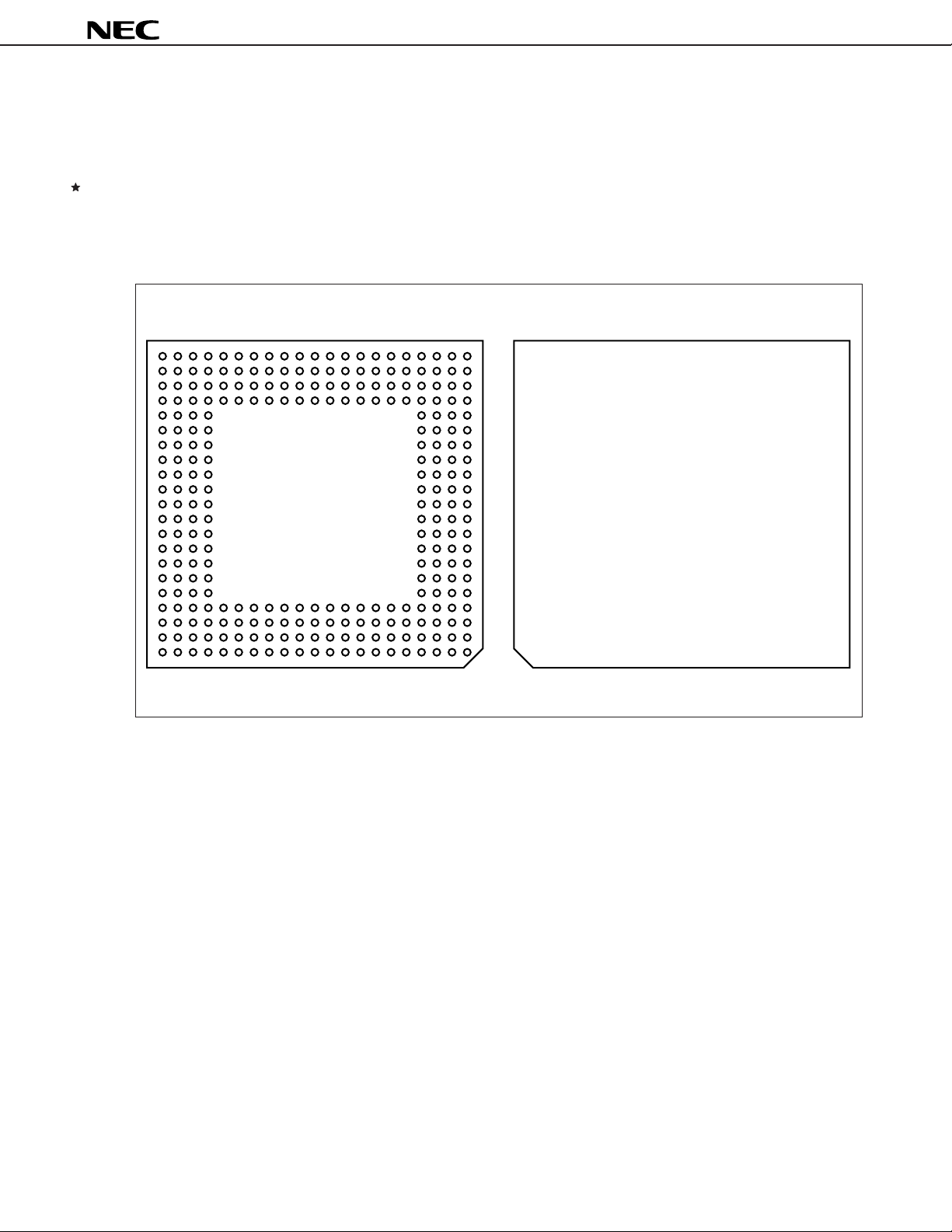
PIN CONFIGURATION
• 223-pin ceramic PGA (48 × 48)
µ
PD30500RJ-150
µ
PD30500RJ-180
µ
PD30500RJ-200
Bottom View Top View
18
17
16
15
14
13
12
11
10
9
8
7
6
5
4
3
2
1
µ
PD30500, 30500A, 30500B
ABCDEFGHJKLMNPRTUV
Index mark
VUTRPNMLKJHGFEDCBA
Data Sheet U12031EJ4V0DS00
3
Page 4

µ
PD30500, 30500A, 30500B
No. Name No. Name No. Name No. Name No. Name No. Name
A2 VDD
A3 GND
A4 VDD
A5 GND
A6 GND
A7 VDD
A8 GND
A9 VDD
A10 GND
A11 VDD
A12 GND
A13 VDD
A14 GND
A15 GND
A16 VDD
A17 GND
A18 GND
B1 GND
B2 GND
B3 VDD
B4 SysADC4
B5 SysADC0
B6 SysAD18
B7 SysAD20
B8 SysAD54
B9 SysAD26
B10 SysAD58
B11 SysAD30
B12 SysAD46
B13 SysAD12
B14 SysAD40
B15 SysAD6
B16 GND
B17 VDD
B18 VDD
C1 VDD
C2 VDD
C3 ValidOut
C4 NMI
C5 SysADC6
C6 SysAD16
C7 SysAD50
C8 SysAD22
C9 SysAD24
C10 SysAD28
C11 SysAD62
C12 SysAD44
C13 SysAD10
C14 SysAD38
C15 SysAD4
C16 SysAD34
C17 SysAD2
C18 GND
D1 GND
D2 Int3
D3 Int5
D4 Release
D5 VDD
D6 SysADC2
D7 SysAD48
D8 SysAD52
D9 SysAD56
D10 SysAD60
D11 SysAD14
D12 SysAD42
D13 SysAD8
D14 SysAD36
D15 ColdReset
D16 SysAD0
D17 ScTOE
D18 VDD
E1 GND
E2 Int0
E3 Int2
E4 Int4
E15 SysAD32
E16 ScDCE1
E17 ScCWE1
E18 VDD
F1 VDD
F2 Reserved
F3 ScValid
F4 Int1
F15 ScDCE0
F16 ScCWE0
F17 ScTDE
F18 GND
G1 GND
G2 Reserved
G3 Reserved
G4 Reserved
G15 ScCLR
G16 ScTCE
G17 Modeln
G18 VDD
H1 VDD
H2 Reserved
H3 Reserved
H4 Reserved
H15 VDDOk
H16 ModeClock
H17 SysClock
H18 GND
J1 GND
J2 WrRdy
J3 Validln
J4 ExtRqst
J15 Reserved
J16 Reserved
J17 Reserved
J18 VDD
K1 VDD
K2 ScMatch
K3 RdRdy
K4 ScDOE
K15 Reserved
K16 VDDP
K17 GNDP
K18 GND
L1 GND
L2 SysCmd8
L3 SysCmd7
L4 SysCmd5
L15 ScLine12
L16 ScLine14
L17 ScLine15
L18 VDD
M1 VDD
M2 SysCmd6
M3 SysCmd4
M4 SysCmd1
M15 ScLine8
M16 ScLine10
M17 ScLine13
M18 GND
N1 GND
N2 SysCmd3
N3 SysCmd2
N4 SysADC7
N15 ScLine5
N16 ScLine7
N17 ScLine11
N18 VDD
P1 VDD
P2 SysCmd0
P3 SysCmdP
P4 SysADC1
P15 ScLine2
P16 ScLine4
P17 ScLine9
P18 GND
R1 VDD
R2 SysADC5
R3 SysADC3
R4 BigEndian
R5 SysAD49
R6 SysAD51
R7 SysAD55
R8 SysAD27
R9 SysAD31
R10 SysAD43
R11 SysAD39
R12 SysAD35
R13 SysAD1
R14 ScWord1
R15 ScLine0
R16 ScLine3
R17 ScLine6
R18 GND
T1 GND
T2 SysAD15
T3 SysAD47
T4 SysAD17
T5 SysAD19
T6 SysAD23
T7 SysAD57
T8 SysAD29
T9 VDD
T10 SysAD45
T11 SysAD41
T12 SysAD7
T13 SysAD5
T14 SysAD33
T15 Reset
T16 ScLine1
T17 VDD
T18 VDD
U1 VDD
U2 VDD
U3 GND
U4 SysAD21
U5 SysAD53
U6 SysAD25
U7 SysAD59
U8 SysAD61
U9 SysAD63
U10 SysAD13
U11 SysAD11
U12 SysAD9
U13 SysAD37
U14 SysAD3
U15 ScWord0
U16 VDD
U17 GND
U18 GND
V1 GND
V2 GND
V3 VDD
V4 GND
V5 GND
V6 VDD
V7 GND
V8 VDD
V9 GND
V10 VDD
V11 GND
V12 VDD
V13 GND
V14 VDD
V15 GND
V16 GND
V17 VDD
V18 GND
4
Data Sheet U12031EJ4V0DS00
Page 5
• 272-pin plastic BGA (C/D advanced type) (29 × 29)
µ
PD30500S2-150
µ
PD30500S2-180
µ
PD30500S2-200
µ
PD30500AS2-250
µ
PD30500BS2-300
Note
Bottom View Top View
21
20
19
18
17
16
15
14
13
12
11
10
9
8
7
6
5
4
3
2
1
µ
PD30500, 30500A, 30500B
AAYWVUTRPNMLKJHGFEDCBA ABCDEFGHJKLMNPRTUVWYAA
Note Under development
Data Sheet U12031EJ4V0DS00
5
Page 6

µ
PD30500, 30500A, 30500B
(1)µPD30500
No. Name No. Name No. Name No. Name No. Name No. Name
A1 GND
A2 VDD
A3 GND
A4 SysAD32
A5 GND
A6 ScCWE1
A7 GND
A8 VDDOk
A9 GND
A10 SysClock
A11 GND
A12 ScLine15
A13 GND
A14 ScLine12
A15 GND
A16 ScLine7
A17 GND
A18 ScLine2
A19 GND
A20 VDD
A21 GND
B1 VDD
B2 VDD
B3 VDD
B4 SysAD2
B5 SysAD0
B6 ScTOE
B7 ScCLR
B8 ScTDE
B9 ModeClock
B10 Reserved
B11 Reserved
B12 NC
B13 ScLine14
B14 ScLine10
B15 ScLine9
B16 ScLine6
B17 ScLine3
B18 ScLine1
B19 VDD
B20 VDD
B21 VDD
C1 GND
C2 VDD
C3 ColdReset
C4 SysAD34
C5 ScDCE1
C6 ScDCE0
C7 ScCWE0
C8 ScTCE
C9 Modeln
C10 Reserved
C11 GNDP
C12 Reserved
C13 ScLine13
C14 ScLine11
C15 ScLine8
C16 ScLine5
C17 ScLine4
C18 ScLine0
C19 Reset
C20 VDD
C21 GND
D1 VDD
D2 VDD
D3 VDD
D4 GND
D5 VDD
D6 GND
D7 VDD
D8 VDD
D9 GND
D10 VDD
D11 VDDP
D12 VDD
D13 GND
D14 VDD
D15 VDD
D16 GND
D17 VDD
D18 GND
D19 VDD
D20 VDD
D21 VDD
E1 GND
E2 SysAD36
E3 SysAD4
E4 VDD
E18 VDD
E19 ScWord1
E20 ScWord0
E21 GND
F1 SysAD8
F2 SysAD38
F3 SysAD6
F4 GND
F18 GND
F19 SysAD1
F20 SysAD33
F21 SysAD3
G1 GND
G2 SysAD10
G3 SysAD40
G4 VDD
G18 VDD
G19 SysAD35
G20 SysAD5
G21 GND
H1 SysAD42
H2 SysAD44
H3 SysAD12
H4 VDD
H18 VDD
H19 SysAD7
H20 SysAD39
H21 SysAD37
J1 GND
J2 SysAD46
J3 SysAD14
J4 GND
J18 GND
J19 SysAD9
J20 SysAD41
J21 GND
K1 SysAD60
K2 SysAD30
K3 SysAD62
K4 VDD
K18 VDD
K19 SysAD11
K20 SysAD43
K21 SysAD13
L1 GND
L2 SysAD58
L3 SysAD28
L4 VDD
L18 VDD
L19 SysAD45
L20 SysAD63
L21 GND
M1 SysAD26
M2 SysAD56
M3 SysAD24
M4 VDD
M18 VDD
M19 SysAD29
M20 SysAD61
M21 SysAD31
N1 GND
N2 SysAD54
N3 SysAD22
N4 GND
N18 GND
N19 SysAD27
N20 SysAD59
N21 GND
P1 SysAD50
P2 SysAD52
P3 SysAD20
P4 VDD
P18 VDD
P19 SysAD25
P20 SysAD57
P21 SysAD55
R1 GND
R2 SysAD18
R3 SysAD48
R4 VDD
R18 VDD
R19 SysAD53
R20 SysAD23
R21 GND
T1 SysAD16
T2 SysADC0
T3 SysADC2
T4 GND
T18 GND
T19 SysAD19
T20 SysAD51
T21 SysAD21
U1 GND
U2 SysADC4
U3 SysADC6
U4 VDD
U18 VDD
U19 SysAD17
U20 SysAD49
U21 GND
V1 VDD
V2 VDD
V3 VDD
V4 GND
V5 NMI
V6 GND
V7 VDD
V8 VDD
V9 GND
V10 VDD
V11 VDD
V12 VDD
V13 GND
V14 VDD
V15 VDD
V16 GND
V17 VDD
V18 GND
V19 VDD
V20 VDD
V21 VDD
W1 GND
W2 VDD
W3 VDD
W4 VDD
W5 Int5
W6 Int4
W7 Int1
W8 Reserved
W9 Reserved
W10 Reserved
W11 Validln
W12 ScDOE
W13 SysCmd7
W14 SysCmd4
W15 SysCmd1
W16 SysADC7
W17 SysADC5
W18 SysAD47
W19 BigEndian
W20 VDD
W21 GND
Y1 VDD
Y2 VDD
Y3 VDD
Y4 Release
Y5 Int3
Y6 Int2
Y7 ScValid
Y8 Reserved
Y9 Reserved
Y10 Reserved
Y11 ExtRqst
Y12 RdRdy
Y13 SysCmd8
Y14 SysCmd5
Y15 SysCmd3
Y16 SysCmd0
Y17 SysCmdP
Y18 SysADC1
Y19 SysAD15
Y20 VDD
Y21 VDD
AA1 GND
AA2 VDD
AA3 GND
AA4 ValidOut
AA5 GND
AA6 Int0
AA7 GND
AA8 Reserved
AA9 GND
AA10 WrRdy
AA11 GND
AA12 ScMatch
AA13 GND
AA14 SysCmd6
AA15 GND
AA16 SysCmd2
AA17 GND
AA18 SysADC3
AA19 GND
AA20 VDD
AA21 GND
6
Data Sheet U12031EJ4V0DS00
Page 7

µ
PD30500, 30500A, 30500B
(2)µPD30500A, 30500B
No. Name No. Name No. Name No. Name No. Name No. Name
A1 GND
A2 VDDIO
A3 GND
A4 SysAD32
A5 GND
A6 ScCWE1
A7 GND
A8 VDDOk
A9 GND
A10 SysClock
A11 GND
A12 ScLine15
A13 GND
A14 ScLine12
A15 GND
A16 ScLine7
A17 GND
A18 ScLine2
A19 GND
A20 VDDIO
A21 GND
B1 VDDIO
B2 VDDIO
B3 VDDIO
B4 SysAD2
B5 SysAD0
B6 ScTOE
B7 ScCLR
B8 ScTDE
B9 ModeClock
B10 GND
B11 GND
B12 GND
B13 ScLine14
B14 ScLine10
B15 ScLine9
B16 ScLine6
B17 ScLine3
B18 ScLine1
B19 VDDIO
B20 VDDIO
B21 VDDIO
C1 GND
C2 VDDIO
C3 ColdReset
C4 SysAD34
C5 ScDCE1
C6 ScDCE0
C7 ScCWE0
C8 ScTCE
C9 Modeln
C10 NC
C11 GNDP
C12 GND
C13 ScLine13
C14 ScLine11
C15 ScLine8
C16 ScLine5
C17 ScLine4
C18 ScLine0
C19 Reset
C20 VDDIO
C21 GND
D1 VDD
D2 VDD
D3 VDD
D4 GND
D5 VDD
D6 GND
D7 VDDIO
D8 VDD
D9 GND
D10 VDDIO
D11 VDDP
D12 VDD
D13 GND
D14 VDDIO
D15 VDD
D16 GND
D17 VDDIO
D18 GND
D19 VDD
D20 VDD
D21 VDD
E1 GND
E2 SysAD36
E3 SysAD4
E4 VDD
E18 VDD
E19 ScWord1
E20 ScWord0
E21 GND
F1 SysAD8
F2 SysAD38
F3 SysAD6
F4 GND
F18 GND
F19 SysAD1
F20 SysAD33
F21 SysAD3
G1 GND
G2 SysAD10
G3 SysAD40
G4 VDDIO
G18 VDDIO
G19 SysAD35
G20 SysAD5
G21 GND
H1 SysAD42
H2 SysAD44
H3 SysAD12
H4 VDD
H18 VDD
H19 SysAD7
H20 SysAD39
H21 SysAD37
J1 GND
J2 SysAD46
J3 SysAD14
J4 GND
J18 GND
J19 SysAD9
J20 SysAD41
J21 GND
K1 SysAD60
K2 SysAD30
K3 SysAD62
K4 VDDIO
K18 VDDIO
K19 SysAD11
K20 SysAD43
K21 SysAD13
L1 GND
L2 SysAD58
L3 SysAD28
L4 VDD
L18 VDD
L19 SysAD45
L20 SysAD63
L21 GND
M1 SysAD26
M2 SysAD56
M3 SysAD24
M4 VDDIO
M18 VDDIO
M19 SysAD29
M20 SysAD61
M21 SysAD31
N1 GND
N2 SysAD54
N3 SysAD22
N4 GND
N18 GND
N19 SysAD27
N20 SysAD59
N21 GND
P1 SysAD50
P2 SysAD52
P3 SysAD20
P4 VDD
P18 VDD
P19 SysAD25
P20 SysAD57
P21 SysAD55
R1 GND
R2 SysAD18
R3 SysAD48
R4 VDDIO
R18 VDDIO
R19 SysAD53
R20 SysAD23
R21 GND
T1 SysAD16
T2 SysADC0
T3 SysADC2
T4 GND
T18 GND
T19 SysAD19
T20 SysAD51
T21 SysAD21
U1 GND
U2 SysADC4
U3 SysADC6
U4 VDD
U18 VDD
U19 SysAD17
U20 SysAD49
U21 GND
V1 VDD
V2 VDD
V3 VDD
V4 GND
V5 NMI
V6 GND
V7 VDD
V8 VDDIO
V9 GND
V10 VDD
V11 VDDIO
V12 VDD
V13 GND
V14 VDDIO
V15 VDD
V16 GND
V17 VDDIO
V18 GND
V19 VDD
V20 VDD
V21 VDD
W1 GND
W2 VDDIO
W3 VDDIO
W4 VDDIO
W5 Int5
W6 Int4
W7 Int1
W8 GND
W9 GND
W10 VDD
W11 Validln
W12 ScDOE
W13 SysCmd7
W14 SysCmd4
W15 SysCmd1
W16 SysADC7
W17 SysADC5
W18 SysAD47
W19 BigEndian
W20 VDDIO
W21 GND
Y1 VDDIO
Y2 VDDIO
Y3 VDDIO
Y4 Release
Y5 Int3
Y6 Int2
Y7 ScValid
Y8 GND
Y9 GND
Y10 GND
Y11 ExtRqst
Y12 RdRdy
Y13 SysCmd8
Y14 SysCmd5
Y15 SysCmd3
Y16 SysCmd0
Y17 SysCmdP
Y18 SysADC1
Y19 SysAD15
Y20 VDDIO
Y21 VDDIO
AA1 GND
AA2 VDDIO
AA3 GND
AA4 ValidOut
AA5 GND
AA6 Int0
AA7 GND
AA8 GND
AA9 GND
AA10 WrRdy
AA11 GND
AA12 ScMatch
AA13 GND
AA14 SysCmd6
AA15 GND
AA16 SysCmd2
AA17 GND
AA18 SysADC3
AA19 GND
AA20 VDDIO
AA21 GND
Data Sheet U12031EJ4V0DS00
7
Page 8

PIN NAMES
BigEndian: Endian Mode Select
ColdReset: Cold Reset
ExtRqst: External Request
GND: Ground
GNDP: Quiet GND for PLL
Int (0:5): Interrupt Request
ModeClock: Boot Mode Clock
Modeln: Boot Mode Data In
NC: No Connection
NMI: Non-maskable Interrupt Request
RdRdy: Read Ready
Release: Release Interface
Reset: Reset
ScCLR: Secondary Cache Block Clear
ScCWE (0:1): Secondary Cache Write Enable
ScDCE (0:1): Data RAM Chip Enable
ScDOE: Data RAM Output Enable
ScLine (0:15): Secondary Cache Line Index
ScMatch: Secondary Cache Tag Match
ScTCE: Secondary Cache Tag RAM Chip Enable
ScTDE: Secondary Cache Tag RAM Data Enable
ScTOE: Secondary Cache Tag RAM Output Enable
ScValid: Secondary Cache Valid
ScWord (0:1): Secondary Cache Word Index
SysAD (0:63): System Address/Data Bus
SysADC (0:7): System Address/Data Check Bus
SysClock: System Clock
SysCmd (0:8): System Command/Data Identifier
SysCmdP: System Command/Data Identifier Bus Parity
Validln: Valid Input
ValidOut: Valid Output
DD: Power Supply (
V
VDD: Power Supply for Processor Core (µPD30500A, 30500B)
DDIO: Power Supply for Processor I/O (
V
VDDOk: VDD is OK
VDDP: Quiet VDD for PLL
WrRdy: Write Ready
µ
PD30500)
µ
PD30500A, 30500B only)
µ
PD30500, 30500A, 30500B
8
Data Sheet U12031EJ4V0DS00
Page 9

INTERNAL BLOCK DIAGRAM
µ
PD30500, 30500A, 30500B
Data, address
System interface
Instruction cache Data cache
Instruction address
Control
SysClock
Clock
generator
CP0
TLB
Execution unit
Floating-point unit
Pipeline control
Data Sheet U12031EJ4V0DS00
9
Page 10

µ
PD30500, 30500A, 30500B
CONTENTS
1. PIN FUNCTIONS ................................................................................................................................ 11
2. ELECTRICAL SPECIFICATIONS ......................................................................................................13
2.1µPD30500 ....................................................................................................................................................13
2.2µPD30500A..................................................................................................................................................16
2.3µPD30500B (Preliminary) ..........................................................................................................................19
2.4 Test Condition ............................................................................................................................................ 22
2.5 Timing Chart ............................................................................................................................................... 22
3. PACKAGE DRAWING........................................................................................................................27
4. RECOMMENDED SOLDERING CONDITIONS ................................................................................. 29
APPENDIX DIFFERENCES BETWEEN THE VR5000 AND VR4310TM.................................................... 30
10
Data Sheet U12031EJ4V0DS00
Page 11

1. PIN FUNCTIONS
Pin Name I/O Function
SysAD (0:63) I/O System address/data bus.
64-bit bus for communication between processor, secondary cache and external agent.
SysADC (0:7) I/O System address/data check bus.
8-bit bus including check bits for the SysAD bus.
SysCmd (0:8) I/O System command/data ID bus.
9-bit bus for communication of commands and data identifiers between processor
and external agent.
SysCmdP I/O System command/data ID bus parity.
1-bit even number parity bit for the SysCmd bus.
ValidIn Input Valid in.
Signal indicating that external agent has transmitted valid address or data onto
SysAD bus and valid command or data identifier onto SysCmd bus.
ValidOut Output Valid out.
Signal indicating that processor has transmitted valid address or data onto SysAD
bus and valid command or data identifier onto SysCmd bus.
ExtRqst Input External request.
Signal used by external agent to request for its use by system interface.
Release Output Interface release.
Signal indicating that the processor has released the system interface to the slave state.
WrRdy Output Write ready.
Signal indicating that the external agent can accept a processor write request.
RdRdy Input Read ready.
Signal indicating that external agent can accept a processor read request.
ScCLR Output Secondary cache block clear.
Clears all the valid bits of the tag RAM.
ScCWE (0:1) Output Secondary cache write enable.
Write enable signal for the secondary cache RAM.
ScDCE (0:1) Output Data RAM chip select.
Chip select signal for secondary cache RAM.
ScDOE Input Data RAM output enable.
Data output enable signal from the external agent.
ScLine (0:15) Output Secondary cache line index.
Cache line index output of the secondary cache.
ScMatch Input Secondary cache tag match.
Tag match signal from secondary cache tag RAM.
ScTCE Output Secondary cache tag RAM chip select.
Chip select signal of the secondary cache tag RAM.
ScTDE Output Secondary cache tag RAM data enable.
Data enable signal from the secondary cache tag RAM.
ScTOE Output Secondary cache tag RAM output enable.
Output enable signal from the secondary cache tag RAM.
ScWord (0:1) I/O Secondary cache word index.
Signal indicating that the double word of the secondary cache index is correct.
ScValid I/O Secondary cache valid.
Signal indicating that the data of the secondary cache is valid.
µ
PD30500, 30500A, 30500B
Data Sheet U12031EJ4V0DS00
11
Page 12

Pin Name I/O Function
Int (0:5) Input Interrupt.
General-purpose processor interrupt requests whose input statuses can be confirmed by
bits 15 through 10 of cause register.
NMI Input Non-maskable interrupt.
Interrupt request that cannot be masked.
ColdReset Input Cold reset.
Signal initializing the internal status of the processor. Inactivate this signal in synchronization with SysClock.
Reset Input Reset.
Signal generating a reset exception, without initializing the internal status of the processor.
Inactivate this signal in synchronization with SysClock.
SysClock Input System clock.
Clock input signal to processor.
BigEndian Input Endian mode setting.
This signal sets the endian mode of the system interface.
When setting the endian mode with this signal, specify little endian with the data from the
ModeIn pin that is input at reset.
To set the endian mode with the data from the ModeIn pin, fix this signal to 0.
BigEndian Bit 8 of boot mode Mode
11 —
1 0 Big endian
0 1 Big endian
0 0 Little endian
ModeClock Output Boot mode clock.
Successive boot mode data clock output resulting from dividing SysClock by 256.
Modeln Input Boot mode data input.
Input of initialization bit stream.
VDDOk Input VDD and VDDIO
Signal indicating that the voltage supplied to the VR5000 is reached to the rated level
for 100 ms or more, and that that status is stabilized. When VDDOk is asserted active, the
VR5000 starts an initialization sequence.
VDDP – PLL VDD.
Power supply for internal PLL.
GNDP – PLL GND.
Ground for internal PLL.
VDD –• VR5000
Positive power supply pin (3.3 V)
• VR5000A
Power supply pin for core (2.5 V)
• VR5000B
Power supply pin for core (1.8 V)
Note1
VDDIO
GND – Ground pin.
– Power supply pin for I/O (3.3 V)
Note1
are valid.
µ
PD30500, 30500A, 30500B
Note2
Notes 1. VDDIO is only for VR5000A and VR5000B.
2. VR5000: VDD = 3.135 V
V
R5000A: VDD = 2.375 V, VDDIO = 3.135 V
VR5000B: VDD = 1.7 V, VDDIO = 3.135 V
12
Data Sheet U12031EJ4V0DS00
Page 13

µ
PD30500, 30500A, 30500B
2. ELECTRICAL SPECIFICATIONS
2.1µPD30500
Absolute Maximum Ratings
Parameter Symbol Condition Rating Unit
Supply voltage VDD –0.5 to +4.0 V
Input voltage
Operating case temperature TC PGA package 0 to +70 °C
Storage temperature Tstg PGA package –65 to +150 °C
Note The upper limit of the input voltage (VDD + 0.3) is +4.0 V.
Cautions 1. Do not short circuit two or more outputs at the same time.
Note
VI –0.5 to VDD + 0.3 V
Pulse of less than 10 ns –1.5 to VDD + 0.3 V
BGA package 0 to +85 °C
BGA package –40 to +125 °C
2. The quality of the product may be degraded if the absolute maximum rating of even one of
the above parameters is exceeded, even momentarily. Absolute maximum ratings, therefore,
specify the values which if exceeded may physically damage the product. Use the product
never exceeding these ratings.
The specifications and conditions shown in the following DC Characteristics and AC
Characteristics are the range within which the product can normally operate and the quality
can be guaranteed.
DC Characteristics (T
Parameter Symbol Condition MIN. MAX. Unit
High-level output voltage VOH VDD = MIN., IOH = –4 mA 2.4 V
Low-level output voltage VOL VDD = MIN., IOL = 4 mA 0.4 V
High-level input voltage
Low-level input voltage
High-level input voltage
Low-level input voltage
Supply current IDD Normal 150 MHz 2.16 A
Input leakage current ILI –5 +5
Input/output leakage current ILIO –5 +5
C = 0 to +70°C (PGA Package), TC = 0 to +85°C (BGA Package), VDD = 3.3 V ±5%)
Note 1
Note 1
Note 2
Note 2
VIH 2.0 VDD + 0.3 V
VIL –0.5 +0.8 V
Pulse of less than 10 ns –1.5 +0.8 V
VIHC 0.8 × VDD VDD + 0.3 V
VILC –0.5 0.2 × VDD V
Pulse of less than 10 ns –1.5 0.2 × VDD V
operation
Standby 0.25 A
180 MHz 2.54 A
200 MHz 2.8 A
Notes 1. Not applied to the SysClock pin.
2. Applied to the SysClock pin only.
µ
A
µ
A
Remark The operating supply current is almost proportional to the operating clock frequency.
Data Sheet U12031EJ4V0DS00
13
Page 14

µ
PD30500, 30500A, 30500B
Capacitance
Parameter Symbol Condition MIN. MAX. Unit
Input capacitance CIn 5pF
Output capacitance Cout 7pF
AC Characteristics (TC = 0 to +70°C (PGA Package), TC = 0 to +85°C (BGA Package), VDD = 3.3 V ±5%)
Clock parameter
Parameter Symbol Condition MIN. MAX. Unit
System clock high-level width tCH 3.0 ns
System clock low-level width tCL 3.0 ns
System clock frequency
System clock cycle tCP 150 MHz 13.3 50 ns
System clock jitter tji System clock frequency > 66 MHz ±125 ps
System clock rise time tCR 2.0 ns
System clock fall time tCF 2.0 ns
Mode clock cycle tMOC 256 × tCP ns
Notes 1, 2
150 MHz 20 75 MHz
180 MHz 20 90 MHz
200 MHz 20 100 MHz
180 MHz 11.1 50 ns
200 MHz 10 50 ns
System clock frequency ≤ 66 MHz ±250 ps
Notes 1. The operation of the VR5000 is guaranteed only when the PLL is operating
2. The operation is guaranteed if the internal operating frequency 100 MHz or higher.
14
Data Sheet U12031EJ4V0DS00
Page 15

µ
PD30500, 30500A, 30500B
System Interface Parameter
Parameter Symbol Condition MIN. MAX. Unit
Data output hold time tDM Modebit (14 : 13) = 10 1.0 ns
Modebit (14 : 13) = 11 1.1 ns
Modebit (14 : 13) = 00 1.3 ns
Modebit (14 : 13) = 01 1.3 ns
Data output delay time tDO 5.0 ns
Data input setup time t DS 1.6 ns
Data input hold time tDH 0.5 ns
Boot Mode Interface Parameter
Parameter Symbol Condition MIN. MAX. Unit
More data setup time tMDS tCP × 0.35 ns
Mode data hold time tMDH tCP × 0.35 ns
Load Coefficient
Parameter Symbol Condition MIN. MAX. Unit
Load coefficient CLD 1.5 ns/25 pF
Data Sheet U12031EJ4V0DS00
15
Page 16

µ
PD30500, 30500A, 30500B
2.2µPD30500A
Absolute Maximum Ratings
Parameter Symbol Condition Rating Unit
Supply voltage VDDIO –0.5 to +4.0 V
VDD –0.3 to +3.3 V
Input voltage
Operating case temperature TC 0 to +85 °C
Storage temperature Tstg –40 to +125 °C
Note
VI –0.5 to VDDIO + 0.3 V
Pulse of less than 10 ns –1.5 to VDDIO + 0.3 V
Note The upper limit of the input voltage (VDDIO + 0.3) is +4.0 V.
Cautions 1. Do not short circuit two or more outputs at the same time.
2. The quality of the product may be degraded if the absolute maximum rating of even one of
the above parameters is exceeded, even momentarily. Absolute maximum ratings, therefore,
specify the values which if exceeded may physically damage the product. Use the product
never exceeding these ratings.
The specifications and conditions shown in the following DC Characteristics and AC
Characteristics are the range within which the product can normally operate and the quality
can be guaranteed.
DC Characteristics (T
Parameter Symbol Condition MIN. MAX. Unit
High-level output voltage VOH VDDIO = MIN., IOH = –4 mA 2.4 V
Low-level output voltage VOL VDDIO = MIN., IOL = 4 mA 0.4 V
High-level input voltage
Low-level input voltage
High-level input voltage
Low-level input voltage
Supply current IDD 1.8 A
Input leakage current ILI –5 +5
Input/output leakage current ILIO –5 +5
C = 0 to +85°C, VDDIO = 3.3 V ±5%, VDD = 2.5 V ±5%)
Note 1
Note 1
Note 2
Note 2
VIH 2.0 VDDIO + 0.3 V
VIL –0.5 +0.8 V
Pulse of less than 10 ns –1.5 +0.8 V
VIHC 0.8 × VDDIO VDDIO + 0.3 V
VILC –0.5 0.2 × VDDIO V
Pulse of less than 10 ns –1.5 0.2 × VDDIO V
IDDIO System clock frequency = 50 MHZ 0.7 A
System clock frequency = 67 MHZ 0.85 A
System clock frequency = 83 MHZ 0.95 A
System clock frequency = 100 MHZ 1.15 A
Notes 1. Not applied to the SysClock pin.
2. Applied to the SysClock pin only.
µ
A
µ
A
16
Data Sheet U12031EJ4V0DS00
Page 17

µ
PD30500, 30500A, 30500B
Power Application Sequence
Two kinds of power sources are provided with the VR5000A. The sequence of the power application order is not
fixed. However, make sure that either of the power supplies does not remain turned on for 1 second or more while
the other remains off.
Parameter Symbol Condition MIN. MAX. Unit
Power application delay tDP 0 1 sec
Capacitance
Parameter Symbol Condition MIN. MAX. Unit
Input capacitance CIn 5pF
Output capacitance Cout 7pF
AC Characteristics (TC = 0 to +85°C, VDDIO = 3.3 V ±5%, VDD = 2.5 V ±5%)
Clock parameter
Parameter Symbol Condition MIN. MAX. Unit
System clock high-level width tCH 3.0 ns
System clock low-level width tCL 3.0 ns
System clock frequency
System clock cycle tCP 10 50 ns
System clock jitter tji System clock frequency > 66 MHz ±125 ps
System clock rise time tCR 2.0 ns
System clock fall time tCF 2.0 ns
Mode clock cycle tMOC 256 × tCP ns
Notes 1, 2
20 100 MHz
System clock frequency ≤ 66 MHz ±250 ps
Notes 1. The operation of the VR5000A is guaranteed only when the PLL is operating
2. The operation is guaranteed if the internal operating frequency 100 MHz or higher.
Data Sheet U12031EJ4V0DS00
17
Page 18

µ
PD30500, 30500A, 30500B
System Interface Parameter
Parameter Symbol Condition MIN. MAX. Unit
Data output hold time tDM Modebit (14 : 13) = 10 1.3 ns
Modebit (14 : 13) = 11 1.4 ns
Modebit (14 : 13) = 00 1.5 ns
Modebit (14 : 13) = 01 1.5 ns
Data output delay time tDO PClock/SysClock division ratio = 5.0 ns
2, 3, 4, 5, 6, 7, 8,
PClock/SysClock division ratio = 2.5 7.0 ns
Data input setup time t DS 1.6 ns
Data input hold time tDH 0.5 ns
Boot Mode Interface Parameter
Parameter Symbol Condition MIN. MAX. Unit
Mode data setup time tMDS tCP × 0.35 ns
Mode data hold time tMDH tCP × 0.35 ns
Load Coefficient
Parameter Symbol Condition MIN. MAX. Unit
Load coefficient CLD 1.5 ns/25 pF
18
Data Sheet U12031EJ4V0DS00
Page 19

µ
PD30500, 30500A, 30500B
2.3µPD30500B (Preliminary)
Absolute Maximum Ratings
Parameter Symbol Condition Rating Unit
Supply voltage VDDIO –0.5 to +4.0 V
VDD –0.3 to +2.5 V
Input voltage
Operating case temperature TC 0 to +85 °C
Storage temperature Tstg –40 to +125 °C
Note
VI –0.5 to VDDIO + 0.3 V
Pulse of less than 10 ns –1.5 to VDDIO + 0.3 V
Note The upper limit of the input voltage (VDDIO + 0.3) is +4.0 V.
Cautions 1. Do not short circuit two or more outputs at the same time.
2. The quality of the product may be degraded if the absolute maximum rating of even one of
the above parameters is exceeded, even momentarily. Absolute maximum ratings, therefore,
specify the values which if exceeded may physically damage the product. Use the product
never exceeding these ratings.
The specifications and conditions shown in the following DC Characteristics and AC
Characteristics are the range within which the product can normally operate and the quality
can be guaranteed.
DC Characteristics (T
Parameter Symbol Condition MIN. MAX. Unit
High-level output voltage VOH VDDIO = MIN., IOH = –4 mA 2.4 V
Low-level output voltage VOL VDDIO = MIN., IOL = 4 mA 0.4 V
High-level input voltage
Low-level input voltage
High-level input voltage
Low-level input voltage
Input leakage current ILI –5 +5
Input/output leakage current ILIO –5 +5
C = 0 to +85°C, VDDIO = 3.3 V ±5%, VDD = 1.8 V ±0.1 V)
Note 1
Note 1
Note 2
Note 2
VIH 2.0 VDDIO + 0.3 V
VIL –0.5 +0.8 V
Pulse of less than 10 ns –1.5 +0.8 V
VIHC 0.8 × VDDIO VDDIO + 0.3 V
VILC –0.5 0.2 × VDDIO V
Pulse of less than 10 ns –1.5 0.2 × VDDIO V
µ
A
µ
A
Notes 1. Not applied to the SysClock pin.
2. Applied to the SysClock pin only.
Power Application Sequence
Two kinds of power sources are provided with the V
R5000B. The sequence of the power application order is not
fixed. However, make sure that either of the power supplies does not remain turned on for 1 second or more while
the other remains off.
Parameter Symbol Condition MIN. MAX. Unit
Power application delay tDP 01se
Data Sheet U12031EJ4V0DS00
19
Page 20

µ
PD30500, 30500A, 30500B
Capacitance
Parameter Symbol Condition MIN. MAX. Unit
Input capacitance CIn 5pF
Output capacitance Cout 7pF
AC Characteristics (TC = 0 to +85°C, VDDIO = 3.3 V ±5%, VDD = 1.8 V ±0.1 V)
Clock parameter
Parameter Symbol Condition MIN. MAX. Unit
System clock high-level width tCH 3.0 ns
System clock low-level width tCL 3.0 ns
System clock frequency
System clock cycle tCP 10 50 ns
System clock jitter tji System clock frequency > 66 MHz ±125 ps
System clock rise time tCR 2.0 ns
System clock fall time tCF 2.0 ns
Mode clock cycle tMOC 256 × tCP ns
Notes 1, 2
20 100 MHz
System clock frequency ≤ 66 MHz ±250 ps
Notes 1. The operation of the VR5000B is guaranteed only when the PLL is operating
2. The operation is guaranteed if the internal operating frequency 100 MHz or higher.
20
Data Sheet U12031EJ4V0DS00
Page 21

µ
PD30500, 30500A, 30500B
System Interface Parameter
Parameter Symbol Condition MIN. MAX. Unit
Data output hold time tDM Modebit (14 : 13) = 10 1.3 ns
Modebit (14 : 13) = 11 1.4 ns
Modebit (14 : 13) = 00 1.5 ns
Modebit (14 : 13) = 01 1.5 ns
Data output delay time tDO 5.0 ns
Data input setup time t DS 1.6 ns
Data input hold time tDH 0.5 ns
Boot Mode Interface Parameter
Parameter Symbol Condition MIN. MAX. Unit
Mode data setup time tMDS tCP × 0.35 ns
Mode data hold time tMDH tCP × 0.35 ns
Load Coefficient
Parameter Symbol Condition MIN. MAX. Unit
Load coefficient CLD 1.5 ns/25 pF
Data Sheet U12031EJ4V0DS00
21
Page 22

2.4 Test Condition
Test point
µ
PD30500, 30500A, 30500B
50%SysClock
t
DO
t
DM
Load Conditions
2.5 Timing Chart
Clock timing
All output pins
All output pins
50%
DUT
L
= 50 pF
C
t
CP
t
CH
80%
22
50%SysClock
20%
t
CL
Data Sheet U12031EJ4V0DS00
CR
t
t
CF
Page 23

Mode clock timing
Clock jitter
µ
PD30500, 30500A, 30500B
t
MOC
50%ModeClock
SysClock
System interface edge timing
SysAD (0 : 63), SysADC (0 : 7),
SysCmd (0 : 8), SysCmdP,
ScLine (0 : 15), ScWord (0 : 1), ScTCE, ScValid
ValidOut, Release, ScCLR,
ScCWE (0 : 1), ScDCE (0 : 1),
SysClock
ScTDE, ScTOE
t
ji
tDM
tDM
t
ji
50%
tDO
tDH
tDS
OutputOutput
tDO
OutputOutput
Input
ValidIn, ExtRqst, RdRdy,
WrRdy, ScDOE, ScMatch,
Int (0 : 5), NMI
Data Sheet U12031EJ4V0DS00
tDS
tDH
Input
23
Page 24

Boot mode interface edge timing
ModeClock
t
MDS
t
MDH
µ
PD30500, 30500A, 30500B
Clocking relations
SysClock
(Input)
PClock
(Output)
SysAD Driven
(Output)
SysAD Received
(Input)
ModeIn
1234Cycle
Input
t
DM
t
DO
Data
Data Data Data Data
DataDataData
Power application sequence (V
24
t
DS
R5000A, VR5000B only)
0.5V
DD
V
VDDIO
DD
0.5VDDIO
Data Sheet U12031EJ4V0DS00
t
DH
t
DP
t
DP
Page 25

Reset Timing
Power-on reset timing
µ
PD30500, 30500A, 30500B
Note 1
DD
3.135 V
VDDI/O
V
Note 2
SysClock
Ok
≥ 100 ms
256 SysClock
V
DD
ModeClock
t
MDS
ModeIn
ColdReset
Reset
Notes 1. 3.135 V (V
R5000), 2.375 V (VR5000A), 1.7 V (VR5000B)
2. VR5000A, VR5000B only
≥ 64 K SysClock
t
MDH
bit0 bit1 bit255
t
DS
Undefined
t
DS
≥ 64 SysClock
Cold reset timing
H
DD
V
Note
VDDIO
SysClock
V
ModeClock
ModeIn
ColdReset
Note V
H
≥ 64 SysClock
DD
Ok
Reset
R5000A, VR5000B only
256 SysClock
t
MDS
≥ 64 K SysClock
t
MDH
bit0 bit1 bit255
t
DS
Undefined
t
≥ 64 SysClock
DS
Data Sheet U12031EJ4V0DS00
25
Page 26

Warm reset timing
V
Note
VDDIO
SysClock
V
DD
Ok
µ
PD30500, 30500A, 30500B
H
DD
H
≥ 64 SysClock
H
ColdReset
Reset
Note VR5000A, VR5000B only
H
t
t
DS
DS
26
Data Sheet U12031EJ4V0DS00
Page 27

3. PACKAGE DRAWING
223 PIN CERAMIC PGA
µ
PD30500, 30500A, 30500B
A
< Bottom View >
18
17
16
15
14
13
12
11
D
10
9
8
7
6
5
4
3
2
1
Index Mark
TSRQPNMLKJHGFEDCBA
J
I
K
L
M
φ
M
F
E
H
G
NOTE
Each lead centerline is located within 0.254( 0.010 inch) of
φφ
its true position (T.P.) at maximum material condition.
ITEM MILLIMETERS INCHES
A
47.24±0.25 1.860±0.010
D
47.24±0.25
E
2.03
F
2.54(T.P.)
G
3.30±0.2
H
0.50 MIN.
I
2.82 0.111
J 3.98 MAX.
K
L 0.46±0.05 0.018±0.002
M 0.254 0.010
1.27±0.2 0.050±0.008
φ
φφ
1.860±0.010
0.080
0.100(T.P.)
0.130±0.008
0.019 MIN.
0.157 MAX.
X223RJ-100A-1
Data Sheet U12031EJ4V0DS00
27
Page 28

272-PIN PLASTIC BGA (C/D advanced type) (29x29)
µ
PD30500, 30500A, 30500B
S
B
Index area
Y
A
A
21
20
19
18
17
16
15
14
13
12
D
AA
VUTRPNMLKJHGFEDCBA
WY
11
10
9
8
7
6
5
4
3
2
1
Z
J
H
detail of A part
G
A
SK
φ
M
L
M
φ
M
S
P
F
A BS
E
N
28
Data Sheet U12031EJ4V0DS00
ITEM MILLIMETERS
29.00±0.20
A
D 29.00±0.20
E 1.80
F 1.27 (T.P.)
G 0.60±0.10
0.90
H
J 1.50±0.20
K 0.15
φ
L
M 0.30
N 0.25 MIN.
P 0.10
Y C1.5
Z C0.5
0.75±0.15
S272S2-127-C6-3
Page 29

µ
PD30500, 30500A, 30500B
4. RECOMMENDED SOLDERING CONDITIONS
Soldering this product under the following soldering conditions is recommended.
For the details of the recommended soldering conditions, refer to Information Document Semiconductor Device
Mounting Technology Manual (C10535E).
For the soldering methods and recommended other than those recommended, consult NEC.
(1) Soldering Conditions of Surface Mount Type
µ
PD30500S2-150: 272-pin plastic BGA (C/D advanced type) (29 × 29)
µ
PD30500S2-180: 272-pin plastic BGA (C/D advanced type) (29 × 29)
µ
PD30500S2-200: 272-pin plastic BGA (C/D advanced type) (29 × 29)
µ
PD30500AS2-250: 272-pin plastic BGA (C/D advanced type) (29 × 29)
µ
PD30500BS2-300
Note 1
: 272-pin plastic BGA (C/D advanced type) (29 × 29)
Soldering Method Soldering Conditions
Infrared reflow Package peak temperature: 235°C, Time: 30 sec max. (210°C min.), IR35-103-3
Number of times: 3 times max., Number of days: 3
necessary at 125°C for 10 hours)
VPS Package peak temperature: 215°C, Time: 25 to 40 sec max. (200°C min.), VP15-103-3
Number of times: 3 times max., Number of days: 3
necessary at 125°C for 10 hours)
Partial heating Pin temperature: 300°C max., Time: 3 sec max. (per device side) —
Note 2
(after that, prebaking is
Note 2
(after that, prebaking is
Recommended
Conditions Symbol
Notes 1. Under development
2. Number of days in storage after the dry pack has been opened. The storage conditions are at 25°C, 65% RH
MAX.
Caution Do not use two or more soldering methods in combination (except partial heating).
(2) Soldering Conditions of Insertion Type
µ
PD30500RJ-150: 223-pin ceramic PGA (48 × 48)
µ
PD30500RJ-180: 223-pin ceramic PGA (48 × 48)
µ
PD30500RJ-200: 223-pin ceramic PGA (48 × 48)
Soldering Method Soldering Conditions
Wave soldering Solder bath temperature: 260°C max., Time: 10 sec max.
(Pin only)
Partial heating Pin temperature: 300°C max., Time: 3 sec max. (per pin)
Caution Wave soldering is only for the lead part in order that jet solder cannot contact with the chip directly.
Data Sheet U12031EJ4V0DS00
29
Page 30

µ
PD30500, 30500A, 30500B
APPENDIX DIFFERENCES BETWEEN THE VR5000 AND VR4310
Item VR5000 V R4310
Operating frequency Internal 200 MHz MAX. 167 MHz MAX.
External 100 MHz MAX. 83.3 MHz MAX.
Pipeline 2-way super scalar 5-stage 5-stage pipeline
pipeline
Cache Primary instruction cache 32 Kbytes 16 Kbytes
Primary data cache 32 Kbytes 8 Kbytes
Secondary cache interface Provided None
Data protection Byte parity None
System bus Write data transfer rate 9 types (DDDD/DDxDDx/ 2 types (D/Dxx)
DDxxDDxx/DxDxDxDx/
DDxxxDDxxx/DDxxxxDDxxxx/
DxxDxxDxxDxx/
DDxxxxxxDDxxxxxx/DxxxDxxx)
Initialization pin at reset ModeIn (dedicated serial pin) DivMode (0:2)
Status after last data write Access ends Last data retained when transfer
Integer operation unit Corresponding instruction MIPS I, II, III, IV instruction sets MIPS I, II, III instruction sets
JTAG interface None Provided
SyncOut-SyncIn bus None Provided
Clock interface Multiplication ratio of input 2, 3, 4, 5, 6, 7, 8 1.5, 2, 2.5, 3, 4, 5, 6
to internal
Division ratio of internal to 2, 3, 4, 5, 6, 7, 8 1.5, 2, 2.5, 3, 4, 5, 6
bus
Clock output None TClock
Power management mode Standby mode (pipline does Not provided
not operate)
PRId register Imp = 0x23 Imp = 0x0B
TM
rate is set
30
Data Sheet U12031EJ4V0DS00
Page 31

[MEMO]
µ
PD30500, 30500A, 30500B
Data Sheet U12031EJ4V0DS00
31
Page 32

[MEMO]
µ
PD30500, 30500A, 30500B
32
Data Sheet U12031EJ4V0DS00
Page 33

[MEMO]
µ
PD30500, 30500A, 30500B
Data Sheet U12031EJ4V0DS00
33
Page 34

µ
PD30500, 30500A, 30500B
NOTES FOR CMOS DEVICES
1 PRECAUTION AGAINST ESD FOR SEMICONDUCTORS
Note:
Strong electric field, when exposed to a MOS device, can cause destruction of the gate oxide and
ultimately degrade the device operation. Steps must be taken to stop generation of static electricity
as much as possible, and quickly dissipate it once, when it has occurred. Environmental control
must be adequate. When it is dry, humidifier should be used. It is recommended to avoid using
insulators that easily build static electricity. Semiconductor devices must be stored and transported
in an anti-static container, static shielding bag or conductive material. All test and measurement
tools including work bench and floor should be grounded. The operator should be grounded using
wrist strap. Semiconductor devices must not be touched with bare hands. Similar precautions need
to be taken for PW boards with semiconductor devices on it.
2 HANDLING OF UNUSED INPUT PINS FOR CMOS
Note:
No connection for CMOS device inputs can be cause of malfunction. If no connection is provided
to the input pins, it is possible that an internal input level may be generated due to noise, etc., hence
causing malfunction. CMOS devices behave differently than Bipolar or NMOS devices. Input levels
of CMOS devices must be fixed high or low by using a pull-up or pull-down circuitry. Each unused
pin should be connected to V
being an output pin. All handling related to the unused pins must be judged device by device and
related specifications governing the devices.
DD or GND with a resistor, if it is considered to have a possibility of
3 STATUS BEFORE INITIALIZATION OF MOS DEVICES
Note:
Power-on does not necessarily define initial status of MOS device. Production process of MOS
does not define the initial operation status of the device. Immediately after the power source is
turned ON, the devices with reset function have not yet been initialized. Hence, power-on does
not guarantee out-pin levels, I/O settings or contents of registers. Device is not initialized until the
reset signal is received. Reset operation must be executed immediately after power-on for devices
having reset function.
Note that this document is not designated as ‘preliminary’, while some of the related documents are preliminary
versions.
R3000, VR4000, VR4310, VR5000, VR5000A, VR5000B, VR10000, and VR Series are trademarks of NEC
V
Corporation.
MIPS is a trademark of MIPS Technologies Inc.
34
Data Sheet U12031EJ4V0DS00
Page 35

µ
PD30500, 30500A, 30500B
Regional Information
Some information contained in this document may vary from country to country. Before using any NEC
product in your application, please contact the NEC office in your country to obtain a list of authorized
representatives and distributors. They will verify:
• Device availability
• Ordering information
• Product release schedule
• Availability of related technical literature
• Development environment specifications (for example, specifications for third-party tools and
components, host computers, power plugs, AC supply voltages, and so forth)
• Network requirements
In addition, trademarks, registered trademarks, export restrictions, and other legal issues may also vary
from country to country.
NEC Electronics Inc. (U.S.)
Santa Clara, California
Tel: 408-588-6000
800-366-9782
Fax: 408-588-6130
800-729-9288
NEC Electronics (Germany) GmbH
Duesseldorf, Germany
Tel: 0211-65 03 02
Fax: 0211-65 03 490
NEC Electronics (UK) Ltd.
Milton Keynes, UK
Tel: 01908-691-133
Fax: 01908-670-290
NEC Electronics (Germany) GmbH
Benelux Office
Eindhoven, The Netherlands
Tel:040-2445845
Fax: 040-2444580
NEC Electronics (France) S.A.
Velizy-Villacoublay, France
Tel:01-30-67 58 00
Fax: 01-30-67 58 99
NEC Electronics (France) S.A.
Spain Office
Madrid, Spain
Tel: 91-504-2787
Fax: 91-504-2860
NEC Electronics Hong Kong Ltd.
Hong Kong
Tel:2886-9318
Fax: 2886-9022/9044
NEC Electronics Hong Kong Ltd.
Seoul Branch
Seoul, Korea
Tel: 02-528-0303
Fax: 02-528-4411
NEC Electronics Singapore Pte. Ltd.
United Square, Singapore 1130
Tel:65-253-8311
Fax: 65-250-3583
NEC Electronics Taiwan Ltd.
NEC Electronics Italiana s.r.l.
Milano, Italy
Tel: 02-66 75 41
Fax: 02-66 75 42 99
NEC Electronics (Germany) GmbH
Scandinavia Office
Taeby, Sweden
Tel: 08-63 80 820
Fax: 08-63 80 388
Taipei, Taiwan
Tel: 02-2719-2377
Fax: 02-2719-5951
NEC do Brasil S.A.
Electron Devices Division
Rodovia Presidente Dutra, Km 214
07210-902-Guarulhos-SP Brasil
Tel: 55-11-6465-6810
Fax: 55-11-6465-6829
J99.1
Data Sheet U12031EJ4V0DS00
35
Page 36

µ
PD30500, 30500A, 30500B
Exporting this product or equipment that includes this product may require a governmental license from the U.S.A. for some
countries because this product utilizes technologies limited by the export control regulations of the U.S.A.
• The information in this document is subject to change without notice. Before using this document, please
confirm that this is the latest version.
• No part of this document may be copied or reproduced in any form or by any means without the prior written
consent of NEC Corporation. NEC Corporation assumes no responsibility for any errors which may appear in
this document.
• NEC Corporation does not assume any liability for infringement of patents, copyrights or other intellectual
property rights of third parties by or arising from use of a device described herein or any other liability arising
from use of such device. No license, either express, implied or otherwise, is granted under any patents, copyrights
or other intellectual property rights of NEC Corporation or others.
• Descriptions of circuits, software, and other related information in this document are provided for illustrative
purposes in semiconductor product operation and application examples. The incorporation of these circuits,
software, and information in the design of the customer's equipment shall be done under the full responsibility
of the customer. NEC Corporation assumes no responsibility for any losses incurred by the customer or third
parties arising from the use of these circuits, software, and information.
• While NEC Corporation has been making continuous effort to enhance the reliability of its semiconductor devices,
the possibility of defects cannot be eliminated entirely. To minimize risks of damage or injury to persons or
property arising from a defect in an NEC semiconductor device, customers must incorporate sufficient safety
measures in its design, such as redundancy, fire-containment, and anti-failure features.
• NEC devices are classified into the following three quality grades:
"Standard", "Special", and "Specific". The Specific quality grade applies only to devices developed based on a
customer designated “quality assurance program“ for a specific application. The recommended applications of
a device depend on its quality grade, as indicated below. Customers must check the quality grade of each device
before using it in a particular application.
Standard: Computers, office equipment, communications equipment, test and measurement equipment,
audio and visual equipment, home electronic appliances, machine tools, personal electronic
equipment and industrial robots
Special: Transportation equipment (automobiles, trains, ships, etc.), traffic control systems, anti-disaster
systems, anti-crime systems, safety equipment and medical equipment (not specifically designed
for life support)
Specific: Aircraft, aerospace equipment, submersible repeaters, nuclear reactor control systems, life
support systems or medical equipment for life support, etc.
The quality grade of NEC devices is "Standard" unless otherwise specified in NEC's Data Sheets or Data Books.
If customers intend to use NEC devices for applications other than those specified for Standard quality grade,
they should contact an NEC sales representative in advance.
M7 98.8
 Loading...