

DATA SHEET
DATA SHEET
CMOS DIGITAL INTEGRATED CIRCUITS
PPPP
PD2845GR
1 V, 1.3 mA, 94MHz PLL SYNTHESIZER LSI
FOR PAGER SYSTEM
DESCRIPTION
PD2845GR is a PLL synthesizer LSI for pager system. This LSI is manufactured using low voltage CMOS
P
process and therefore realized the low power consumption PLL operated on 1 V, 1.3 mA. This LSI is packaged in 16
pin plastic SSOP suitable for high-density surface mounting. So, this product contributes to produce a long-lifebattery and physically-small pager system.
FEATURES
• Operating frequency : · Input frequency : fin = 10 MHz to 94 MHz
· Reference oscillating frequency : f
• Low Supply voltage : · PLL block : V
· Charge pump block: V
• Low power consumption • I
• Equipped with power-save function • Serial data can be received in power-save mode.
• Packaged in 16 pin plastic SSOP suitable for high-density surface mounting.
DD
= 1.3 mA TYP. @ fin = 70 MHz, f
DD1
= 1.00 V to 1.15 V @ fin = 10 MHz to 70 MHz
DD1
V
= 1.05 V to 1.15 V @ fin = 10 MHz to 94 MHz
DD2
= 3.0 V ± 300 mV
x’tal
= 12.8 MHz
x’tal
= 12.8 MHz
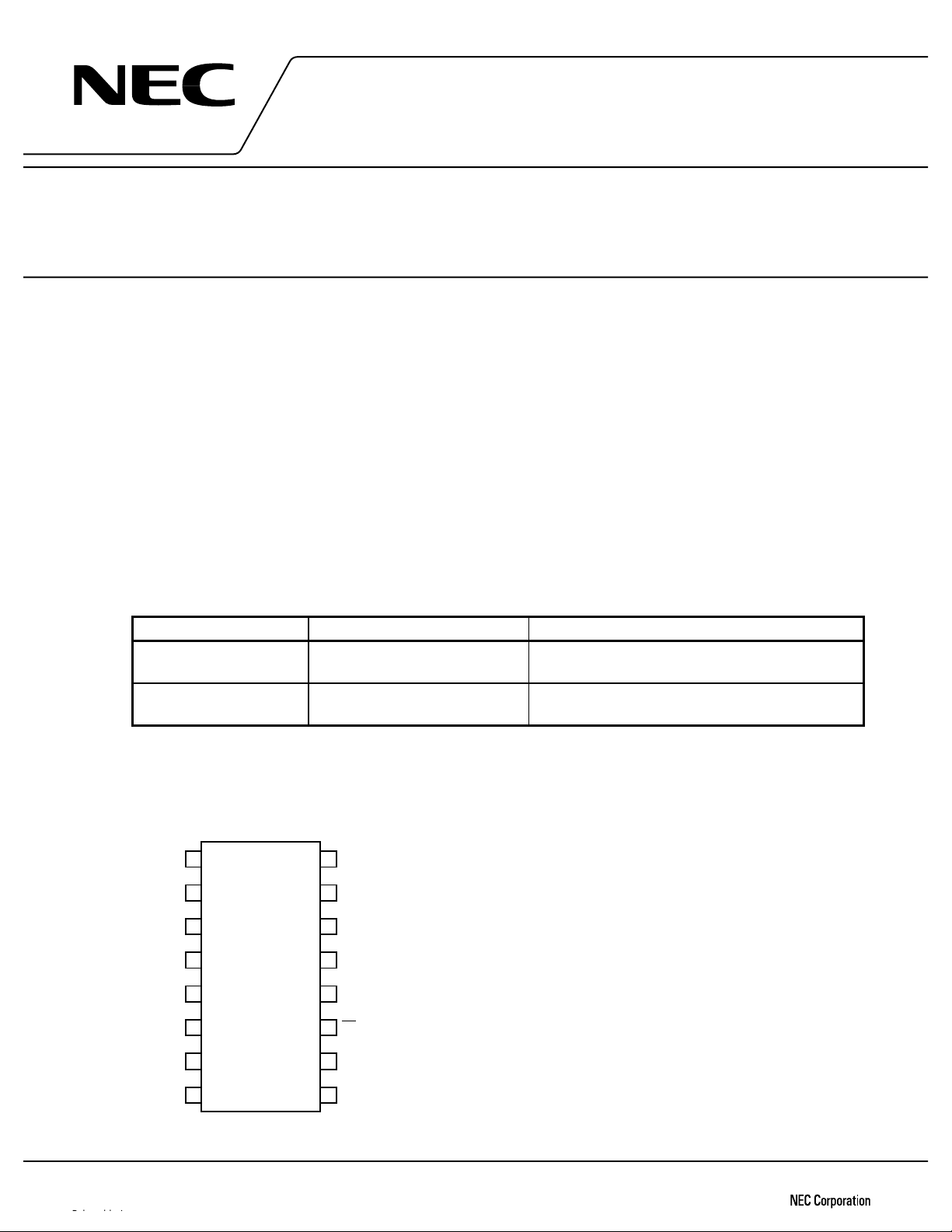
ORDERING INFORMATION
PART NUMBER PACKAGE SUPPLYING FORM
P
PD2845GR-E1 16 pin plastic SSOP
(225 mil)
P
PD2845GR-E2 16 pin plastic SSOP
(225 mil)
* To order evaluation samples, please contact your local NEC sales office (Order number : PPD2845GR).
Embossed tape 12 mm wide. QTY 2.5 k/reel
Pin 1 is in tape pull-out direction.
Embossed tape 12 mm wide. QTY 2.5 k/reel
Pin 1 is in tape roll-in direction.
PIN ASSIGNMENT
(Top View)
V
DD1
F
GND
FR
RESET
EO
IN
XI
XO
LE
CLK
DATA
PS
EOP
EON
Document No. P12150EJ2V0DS00 (2nd edition)
(Previous No. IC-3291)
Date Published February 1997 N
NC
V
DD2
Caution Electro-static sensitive devices
1994©
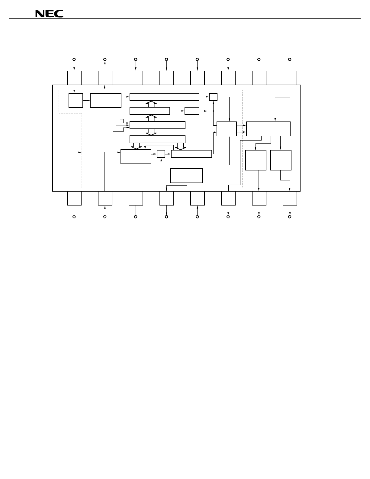
INTERNAL BLOCK DIAGRAM
PPPP
PD2845GR
XI XO LE
16 15 14 13 12 11 10 9
IN
AMP
1 2 3 4 5 6 7 8
V
DD1
1/2
PRESCALER
DATA
CLK
LE
F
IN
5 BIT
reference divider 13 BIT
latch 13 BIT
Shift register 23 BIT
32/33
PRESCALER
GND FR RESET EO EOP EON
CLK
latch 18 BIT
gate
DATA
gate
timer
divider 13 BIT
TEST CIRCUIT
FV
PS NC V
FR
Phase
comparator
Phase detector
error out
Pch
open
drain
Nch
open
drain
DD2
2
PPPP
PD2845GR
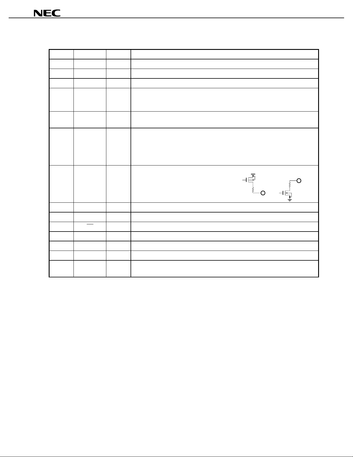
PIN EXPLANATION
PIN No. PIN NAME I/O EXPLANATION FOR FUNCTION
1V
2FINI Frequency Input
3 GND
4 FR O Test pin for monitor.
5 RESET I Test pin for monitor reset. (Refer to RESET on 12 page)
6 EO O Internal charge pump output. In the case of passive filter, this output should be used.
7
8
DD1
EOP
EON
•
•
O
O
Supply voltage to PLL block
Ground
Normally used as PLL, output L should be selected by test bit and this pin should be
opened. (Refer to setting for reference counter on 11 page)
Normally used as PLL, this pin should be grounded.
p
Input signal phase f
fp > fr : Low output
p
< fr : High output
f
p
= fr : High-impedance
f
Outputs for external charge pump. In the case of active filter, this outputs should be used.
EOP : PCH open drain
EON : NCH open drain
vs. reference signal f
r
EON
EOP
9V
10 NC
11 PS I Control bias input for power-save (Refer to Power-save on 12 page).
12 DATA I Data input for divided ratio.
13 CLK I Clock input for shift register.
14 LE I Latch enable input.
15
16
DD2
XO
XI
•
•
O
Supply voltage to charge pump.
Non Connection.
X’tal oscillator connection pin.
I
3
PPPP
PD2845GR
ABSOLUTE MAXIMUM RATINGS (UNLESS OTHERWISE SPECIFIED, TA = +25 °C
Supply Voltage V
Input Voltage V
Output Voltage V
Output Current I
Operating Ambient Temperature T
Storage Temperature T
DD1
DD2
V
I1
I2
V
O1
O2
V
O
A
stg
0.3 to 2.0 V
ð
0.3 to 6.0 V
ð
0.3 to V
ð
0.3 to 6.0 (DATA, CLK, LE, PS) V
ð
0.3 to V
ð
0.3 to V
ð
DD1
+0.3 (Except for DATA, CLK, LE, PS pin) V
DD1
+0.3 (XO, FR) V
DD2
+0.3 (EO, EOP, EON) V
10 mA
10 to +50 °C
ð
55 to +125 °C
ð
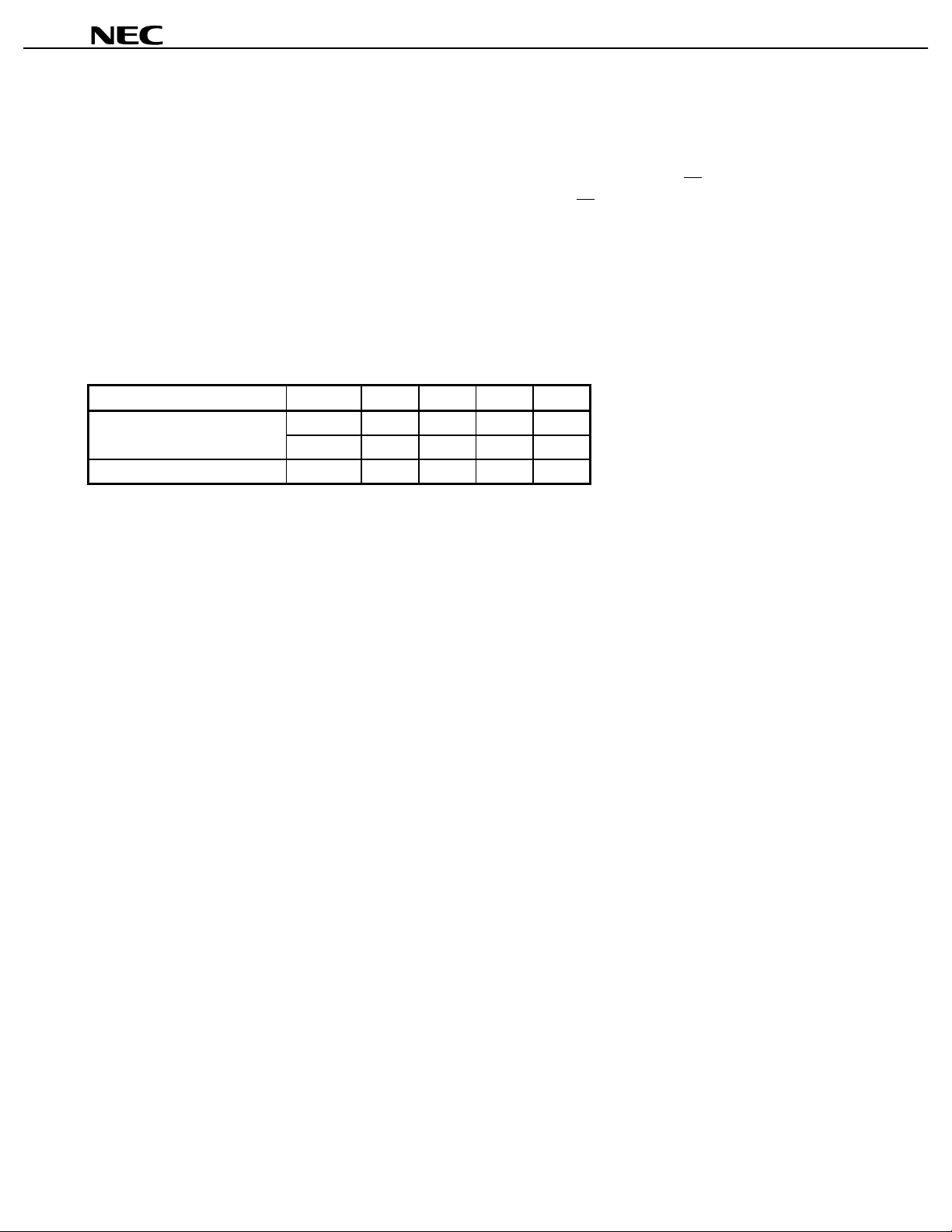
RECOMMENDED OPERATING RANGE
PARAMETER SYMBOL MIN. TYP. MAX. UNIT
DD1
Supply Voltage
Operating Ambient Temperature T
V
V
DD2
A
1.0 1.05 1.1 V
2.85 3.0 3.15 V
10 +25 +50 °C
ð
)
4
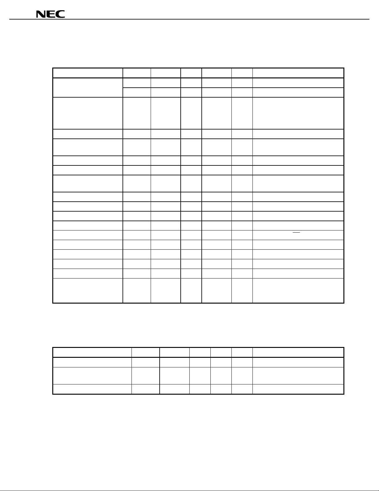
ELECTRICAL CHARACTERISTICS
PPPP
PD2845GR
DC PERFORMANCE (Unless otherwise specified, V
PARAMETER SYMBOL MIN. TYP. MAX. UNIT CONDITIONS
Supply Voltage V
Circuit Current I
Data Retain Current I
High Level Output Current1
High Level Output Current2
High Level Output Current3
Low Level Output Current1
Low Level Output Current2
Low Level Output Current3
High Level Input Current1
Low Level Input Current1
High Level Input Current2
*1
*1
*1
*2
*2
*2
*2
*1
*2
High Level Input Voltage1 V
Low Level Input Voltage1 V
High Level Input Voltage2 V
Low Level Input Voltage2 V
Output Leak Current I
DD1
DD2
V
DD1
DR
OH1
I
OH2
I
OH3
I
OL1
I
OL2
I
OL3
I
IH1
I
IL1
I
IH2
I
IH1
IL1
IH2
IL2
L
1.00 1.05 1.15 V PLL Operation
2.70 3.0 3.30 V P/D Charge pump block
1.0 mA EO, EOP pin. V
ð
0.5 mA XO pin. V
ð
0.1 mA FR pin. V
ð
1.0 mA EO, EON pin. V
0.4 mA XO pin. VOL = 0.5 V
0.4 mA FR pin. VOL = 0.5 V
0.4
0.4
ð
DD1
0.8 u V
0 0.2 u V
DD1
0.8 u V
0 0.2 u V
DD1
= 1.00 V to 1.15 V, V
DD2
= 2.70 to 3.30 V, TA =
1.3 2.2 mA fin = 70 MHz, 0.2 V
fx’tal = 12.8 MHz X’tal OSC IN.
DD1
= 1.0 V to 1.1 V
V
DD2
= 2.85 V to 3.15 V
V
1.0 10
1.0
A No Input Signal, V
P
OH
DD2
= V
= 0.5 V
ð0.5 V
OH
= V
OH
= V
V
OL
V
AFIN, XI pin. VIH = V
P
AFIN, XI pin. VIL = 0 V, V
P
A DATA, CLK, LE, PS pin. V
P
4.0 V DATA, CLK, LE, PS pin.
10
DD1
DD1
V
DD1
4
ð
1.0
r
V DATA, CLK, LE, PS pin.
V RESET pin.
V RESET pin.
A EO, EOP, EON pin.
P
DD1
= 1.0 V to 1.1 V
V
DD2
= 2.85 V to 3.15 V
V
DD2
DD1
DD1
DD2
P-P
DD1
ð0.5 V
ð0.5 V
DD1
10 to +50 °C)
ðððð
.
= 1.1 V
= 2.85 V
= 2.85 V
1.0 V
DD1
1.0 V
IH1
= 3.85 V
Current from IC
*1
Current into IC
*2
AC PERFORMANCE (Unless otherwise specified, V
PARAMETER SYMBOL MIN. TYP. MAX. UNIT CONDITIONS
Input frequency 1 f
Input frequency 2 f
Reference Oscillating Frequency f
in1
in2
x’tal
10 70 MHz FIN pin, Vin = 0.2 V
10 94 MHz FIN pin, Vin = 0.2 V
DD1
= 1.00 V to 1.15 V, V
DD2
= 2.70 to 3.30 V, TA =
12.8 MHz XI, XO pin
DD1
= 1.05 V to 1.15 V
V
P-P
P-P
,
10 to +50
ðððð
C)
qqqq
5

TEST CIRCUIT
DC measurement
BS2
2
GND
4
5
6
7
8
V
DD1
F
IN
GND
FR
RESET
EO
EOP
EON
PD2845GR
µ
XO
LE
CLK
DATA
PS
NC
V
DD2
PPPP
PD2845GR
relay RL1
C1
X’tal
XI
C2
D1
BS3 GND
16
15
14
13
12
11
10
BS1
AC measurement
V
DD1
V
DD2
1 F
µ
1 F
BNC1
BNC2
relay RL1
Diode D1
Capacitor C1,C2
X’tal
1 000 pF
SW 1
V
DD1
F
IN
GND
FR
RESET
EO
EOP
10 pF
XI
X’tal
XO
10 pF
LE
CLK
DATA
PS
NC
µ
100 pF
50 Ω
SW3
: SRR-204
: 1S945
: 18 pF
: 12.8 MHz
12.8 MHz
SW2
BNC1
: Frequency input
BNC2
: Frequency output
SW1
: switch for voltage on/off
SW2
: Desired for PS mode : Low
SW3
: Desired for reset mode : High
EON
PD2845GR
µ
V
DD2
100 pF
6

APPLICATION CIRCUIT EXAMPLES
Passive filter application example (using internal charge pump)
V
DD1
1 F
µ
V
DD2
100 pF
1 000 pF
V
DD1
F
IN
GND
1 F
µ
VCO out
VCO
XO
LE
PPPP
PD2845GR
10 pF
XI
X’tal
12.8 MHz
10 pF
controller
FR
RESET
EO
passive filter
EOP
EON
PD2845GR
µ
Active filter application example (using external charge pump)
IN
(2 pin)
F
VCO
LPF
PMOS
NMOS
CLK
DATA
PS
NC
V
DD2
EO
EOP
EON
100 pF
V
DD1
V
DD2
X’tal
: 1.0 to 1.1 V
: 2.85 to 3.15 V
: 12.8 MHz
7

INPUT TIMING OF SERIAL DATA
DATA
latch
PPPP
PD2845GR
CLK
LE
This logic circuit is controlled by a 3-wire serial bus interface with DATA (12 pin), CLK (13 pin) and LE (14 pin).
On the control setting, Binary-coded serial data is input to DATA pin. This data is read into the shift register at the
rising edge of the CLK signal input to the CLK pin. When the LE signal is at the low level, DATA CLK are received
into the LSI to be latched at the rising edge of the LE signal.
While the LE signal is at the high level, neither DATA nor CLK signals can be received.
CAUTION At the initial V
the non-data input stage. [Refer to ‘Power-save (pin 11)’ on 12 page]
read
CC
supplied time, serial data must be input, because the IC output is unstable on
8

PPPP
PD2845GR
INPUT SIGNAL DIVIDER
INPUT SIGNAL DIVIDER obtain the frequency: fp input to phase comparator. This circuit divides input frequency:
fin to obtain fp. This block consists of prescaler, 5 bit swallow counter, 13 bit main counter and divide-ratio control
circuit.
Setting numbers
• Main counter M = 32 to 8 191
• Swallow counter S = 0 to 31
• Prescaler P = 32, P+1 = 33
Total divide ratio
NT = S(P+1) + P(MðS) = PM+S = 32 M+S (M t S)
NT = 1 024 to 262 143
?
p
in
Relation between f
fp = fin/(32 M+S)
(ex)
At fp = 5 kHz fin = 70 MHz
NT = 70 M/5 k = 14 000
Therefore 14 000 32 = 437 • • • 16
and f
nn
MS
Reference Counter
Reference Counter obtain the frequency: fr input to phase comparater. This circuit divides the reference
oscillating frequency: f
X’tal
of X’tal or TCXO to obtain fr. This block consists of 13 bit programmable reference counter
and prescaler of divide-by-2.
Setting number
• 13 bit programmable reference counter R = 2 to 8 191
Total reference counter block divide ratio
RT = 2 u R
RT = 4 to 16 382
?
r
X’tal
Relation between f
X’tal
fr = (f
/2)/R
and f
(ex)
fr = 5 kHz f
X’tal
= 12.8 MHz
R = (12.8 MHz/2)/5 kHz = 1 280
9

Data format of shift register
Foundaly constraction of shift register
PPPP
PD2845GR
LE
LSB
DATA
CLK
A D22D21D20D19D18D17D16D15D14D13D12D11D10 D9 D8 D7 D6 D5 D4 D3 D2 D1
last bit
(1) Setting for data selection bit
Data selection bit: last A bit can govern the latch selection.
Data selection bit’s construction and function
A Function
1 Setting for swallow and main counter’s divide ratio.
Setting for charge pump output selection.
0 Setting for reference counter’s divide ratio.
“0” = Low, “1” = High
(2) Setting for swallow/main counter’s data and charge pump output selection
Bit constraction of setting for swallow/main counter and charge pump output selection
MSB
first bit
D22A D21 D20 D19 D18 D17 D16 D15 D14 D13 D12 D11 D10 D9 D8 D7 D6 D5 D4 D3 D2 D1
A
A = 1 charge
pump
output
selection
no
assigned
02122232420212223242526272829210211212
2
swallow counter : S
(5 bits 0 to 31)
main counter : M
(13 bits 32 to 8 191)
CAUTION D19, D20 are not assigned for setting but CLK signals must be input because of the bit
construction.
• SWALLOW COUNTER DATA
S = (D14 u 2
4
) + (D15 u 23) + (D16 u 22) + (D17 u 21) + (D18 u 20)
• MAIN COUNTER DATA
M = (D1 u 212) + (D2 u 211) + (D3 u 210) + (D4 u 29) + (D5 u 28) + (D6 u 27) + (D7 u 26) + (D8 u 25) + (D9 u 24) +
(D10 u 23) + (D11 u 22) + (D12 u 21) + (D13 u 20)
10

PPPP
PD2845GR
NT = 32M + S
= 32 u {(D1 u 212) + (D2 u 211) + (D3 u 210) + (D4 u 29) + (D5 u 28) + (D6 u 27) + (D7 u 26) + (D8 u 25) + (D9 u 24) +
(D10 u 23) + (D11 u 22) + (D12 u 21) + (D13 u 20)} + {(D14 u 24) + (D15 u 23) + (D16 u 22) + (D17 u 21) + (D18
20)}
NT = (D1 u 217) + (D2 u 216) + (D3 u 215) + (D4 u 214) + (D5 u 213) + (D6 u 212) + (D7 u 211) + (D8 u 210) + (D9 u 29) +
?
(D10 u 28) + (D11 u 27) + (D12 u 26) + (D13 u 25) + (D14 u 24) + (D15 u 23) + (D16 u 22) + (D17 u 21) + (D18 u 20)
Thus, total divide ratio of input signal divider ‘NT’ can be transferred to binary-code in order to setting data ‘D1 to
D18’ input. (D1 should be top digit and D18 should be bottom digit.)
• Charge pump output selection data
u
D22 D21 EO Pin
(To use internal
charge pump)
0 0 Hi- Impedance OFF
0 1 Hi-Impedance OUTPUT
1 0 OUTPUT OFF
1 1 OUTPUT OUTPUT
EOP, EO Pin
(To use external
charge pump)
“0” = Low, “1” = High
(3) Setting for reference counter
D22A D21 D20 D19 D18 D17 D16 D15 D14 D13 D12 D11 D10 D9 D8 D7 D6 D5 D4 D3 D2 D1
0212223242526272829210211212
2
A
A = 0
(13 bits 2 to 8 191)
01
TEST BIT
(FR pin)
no assignedreference counter : R
CAUTION D1 to D7 are not assigned for setting but CLK signals must be input because of the bit
construction.
RT = 2 u R
RT = 2 u {(D10 u 2
?
12
) + (D11 u 211) + (D12 u 210) + (D13 u 29) + (D14 u 28) + (D15 u 27) + (D16 u 26) + (D17 u 25) +
(D18 u 24) + (D19 u 23) + (D20 u 22) + (D21 u 21) + (D22 u 20)}
*TEST BIT:
for IC tester (FR pin) use or not use (PLL operation).
for normally PLL operation, input D9 = 0, D8 = 1 (FR pin = output L).
11

PPPP
PD2845GR
Power-save and RESET
Power-save (PIN 11)
Power-save-mode can be selected by input data to PS pin.
H; operation mode
L; power-save-mode
On the power-save-mode, reference oscillator and prescaler turn off and error-outs (EO, EOP, EON) output Hi-
impedance but shift register data is remained. Serial data can be received in power-save-mode.
Power-save usage for initial VCC supplying
Note:
To prevent unstable mode at initial VCC supplying, Power-save-mode must be selected. After counter data
setting, normal operation mode can be selected.
RESET (PIN 5)
Reset-mode can be selected by input data to RESET pin.
H; reset-mode L(GND or Open); Normal operation.
On the reset-mode, reference oscillator/prescalers turn off and error-outs (EO, EOP, EON) output Hi-impedance.
Shift-register data is initialized.
This reset-mode should be used at LSI testing, normally use as PLL, RESET pin should be opened or grounded.
Supplementary explanation:
When RESET pin bias is switched from H to L, initial divide ratios can be set automatically as follows
• Input signal divider: NT = 10372
• 13 bit programmable reference counter: R = 1 280 (RT = 2 560)
These divide ratios make PLL loop without controller on condition as follows
fin = 51.86 MHz
x’tal
f
= 12.8 MHz
fp = fr = 5.0 kHz
12

PHASE COMPARATOR
PHASE COMPARATOR compares the phase between divided input frequency (f
This circuit make the change pump output signals according to following detection.
To use internal charge pump
detection
p
fr > f
p
fr = f
p
fr < f
*3
EO
H H OFF
Hi-Impedance OFF OFF
L OFF L
EOP
*4
EON
*4
*3
(passive filter type)
To use external charge pump
*4
(active filter type)
VCO should be used as type of ‘higher voltagehigher frequency’.
EO
EOP
PPPP
PD2845GR
p
) and reference frequency (fr).
EON
EOP is Pch open drain, EON is Nch open drain. EO is output pin of internal charge pump.
SYSTEM APPLICATION EXAMPLE
Pager block diagram of direct conversion type
π/2
×5
LPF
PLL
µ
PD2845GR
LPF
∫
DET
DECODER
CLOCK
∫
DRIVER
DRIVER
BZ
LCD
13

PACKAGE DIMENSIONS
16 PIN PLASTIC SHRINK SOP (225 mil)
16 9
detail of lead end
P
PPPP
PD2845GR
18
A
G
F
K
E
C
B
N
DM
NOTE
Each lead centerline is located within 0.10 mm (0.004 inch) of
its true position (T.P.) at maximum material condition.
M
L
H
I
ITEM MILLIMETERS INCHES
A
5.50 MAX.
B
0.475 MAX.
C
0.65 (T.P.)
D 0.20±0.10 0.008±0.004
E
0.125±0.075
F
1.8 MAX.
G
1.44
H
6.2±0.3
I
4.4±0.2
J
0.9±0.2
K 0.15
L 0.5±0.2 0.020
M
N
P5°±5°
+0.10
–0.05
0.10
0.10 0.004
J
0.217 MAX.
0.019 MAX.
0.026 (T.P.)
0.005±0.003
0.071 MAX.
0.057
0.244±0.012
+0.009
0.173
–0.008
+0.009
0.035
–0.008
+0.004
0.006
–0.002
+0.008
–0.009
0.004
5°±5°
P16GM-65-225B-2
14

PPPP
PD2845GR
NOTE ON CORRECT USE
(1) Observe precautions for handling because of electrostatic sensitive devides.
(2) Form a ground pattern as wide as possible to minimize ground impedance.
(3) Connect a bypass capacitor (e. g. 1 000 pF) to the V
(4) The DC cut capacitor must be each attached to FIN, XI and XO pin.
(5) External R, C values of loop filter should be determined according to the VCO specification.
(6) While VCO signal is not input to FIN pin, power-save-mode must be set.
(7) After initially VCC, VDD are supplied, serial data should be input immediately. (Before serial data input, LSI
operation is unstable or undesired.)
DD
pin.
RECOMMENDED SOLDERING CONDITIONS
This product should be soldered in the following recommended conditions. Other soldering method and conditions
than the recommended conditions are to be consulted with our sales representatives.
PD2845GR
PPPP
Soldering process Soldering conditions Symbol
Infrared ray reflow Peak package’s surface temperature: 235 °C or below,
Reflow time: 30 seconds or below (210 °C or higher),
Number of reflow process: 2, Exposure limit*: None
VPS Peak package’s surface temperature: 215 °C or below,
Reflow time: 40 seconds or below (200 °C or higher),
Number of reflow process: 2, Exposure limit*: None
Partial heating method Terminal temperature: 300 °C or below,
Flow time: 3 seconds or below, Exposure limit*: None
*: Exposure limit before soldering after dry-package is opened.
Storage conditions: 25 °C and relative humidity at 65 % or less.
Apply only a single process at once, except for “Partial heating method”.
Note
For details of recommended soldering conditions for surface mounting, refer to information document
SEMICONDUCTOR DEVICE MOUNTING TECHNOLOGY MANUAL (C10535E).
IR35-00-2
VP15-00-2
15

PPPP
PD2845GR
No part of this document may be copied or reproduced in any form or by any means without the prior written
consent of NEC Corporation. NEC Corporation assumes no responsibility for any errors which may appear in this
document.
NEC Corporation does not assume any liability for infringement of patents, copyrights or other intellectual
property rights of third parties by or arising from use of a device described herein or any other liability arising
from use of such device. No license, either express, implied or otherwise, is granted under any patents,
copyrights or other intellectual property rights of NEC Corporation or others.
While NEC Corporation has been making continuous effort to enhance the reliability of its semiconductor devices,
the possibility of defects cannot be eliminated entirely. To minimize risks of damage or injury to persons or
property arising from a defect in an NEC semiconductor device, customers must incorporate sufficient safety
measures in its design, such as redundancy, fire-containment, and anti-failure features.
NEC devices are classified into the following three quality grades:
"Standard", "Special", and "Specific". The Specific quality grade applies only to devices developed based on
a customer designated "quality assurance program" for a specific application. The recommended applications
of a device depend on its quality grade, as indicated below. Customers must check the quality grade of each
device before using it in a particular application.
Standard: Computers, office equipment, communications equipment, test and measurement equipment,
audio and visual equipment, home electronic appliances, machine tools, personal electronic
equipment and industrial robots
Special: Transportation equipment (automobiles, trains, ships, etc.), traffic control systems, anti-disaster
systems, anti-crime systems, safety equipment and medical equipment (not specifically designed
for life support)
Specific: Aircrafts, aerospace equipment, submersible repeaters, nuclear reactor control systems, life
support systems or medical equipment for life support, etc.
The quality grade of NEC devices is "Standard" unless otherwise specified in NEC's Data Sheets or Data Books.
If customers intend to use NEC devices for applications other than those specified for Standard quality grade,
they should contact an NEC sales representative in advance.
Anti-radioactive design is not implemented in this product.
M4 96. 5
 Loading...