

Page 1
DATA SHEET
MOS INTEGRATED CIRCUIT
µ
PD178P018
8-BIT SINGLE-CHIP MICROCONTROLLER
DESCRIPTION
The µPD178P018 is a device in which the on-chip mask ROM of the µPD178018 is replaced with a one-time
PROM or EPROM.
Because this device can be programmed by users, it is ideally suited for system evaluation, small-lot and multiple-
device production, and early development and time-to-market.
The µPD178P018 is a PROM version corresponding to the µPD178004, 178006, and 178016.
µ
Caution The
PD178P018KK-T does not maintain planned reliability when used in your system’s massproduced products. Please use only experimentally or for evaluation purposes during trial manufacture.
For more information on functions, refer to the following User’s Manuals. Be sure to read them when
designing.
µ
PD178018 Subseries User’s Manual: U11410E
78K/0 Series User’s Manual Instruction: U12326E (In Preparation)
FEATURES
• Pin-compatible with mask ROM version (except for VPP pin)
• Internal PROM: 60 Kbytes
•µPD178P018GC : One-time programmable (ideally suited for small-lot production)
•
µ
PD178P018KK-T : Reprogrammable (ideally suited for system evaluation)
• Internal high-speed RAM: 1024 bytes
• Internal expansion RAM: 2048 bytes
• Buffer RAM: 32 bytes
• Can be operated in the same power supply voltage as the mask ROM version
(During PLL operation: V
The electrical specifications (power supply current, etc.) and PLL analog specifications of the
differ from that of mask ROM versions. So, these differences should be considered and verified before
application sets are mass-produced.
DD = 4.5 to 5.5 V)
µ
PD178P018
In this document, the term PROM is used in parts common to one-time PROM versions and EPROM versions.
The information in this document is subject to change without notice.
Document No. U12298EJ1V0DS00 (1st Edition)
Date Published May 1997 N
Printed in Japan
©
1997
Page 2
APPLICATIONS
Car stereo, home stereo systems
ORDERING INFORMATION
Part Number Package Internal ROM Quality Grade
µ
PD178P018GC-3B9 80-pin plastic QFP (14 × 14 mm, 0.65-mm pitch) One-Time PROM Standard
µ
PD178P018KK-T
Note
80-pin ceramic WQFN (14 × 14 mm, 0.65-mm pitch) EPROM Not applicable
Note Under planning
Please refer to "Quality grade on NEC Semiconductor Devices" (Document number C11531E) published by
NEC Corporation to know the specification of quality grade on the devices and its recommended applications.
µ
PD178018 SUBSERIES EXPANSION
PD178P018
80 pins PROM: 60 KB RAM: 3 KB
µ
µ
PD178P018
PD178018 Subseries
µ
80 pins ROM: 60 KB RAM: 3 KBPD178018
80 pins ROM: 48 KB RAM: 3 KB
80 pins ROM: 48 KB RAM: 1 KB
80 pins ROM: 32 KB RAM: 1 KB
µ
PD178016
µ
PD178006
µ
µ
PD178004
2
Page 3
µ
PD178P018
FUNCTION DESCRIPTION
Item Function
Internal memory • PROM : 60 Kbytes
• RAM
High-speed RAM : 1024 bytes
Expansion RAM : 2048 bytes
Buffer RAM : 32 bytes
General register 8 bits × 32 registers (8 bits × 8 registers × 4 banks)
Instruction cycle With variable instruction execution time function
0.44 µs/0.88 µs/1.78 µs/3.56 µs/7.11 µs/14.22 µs (with 4.5-MHz crystal resonator)
Instruction set • 16-bit operation
• Multiply/divide (8 bits × 8 bits, 16 bits ÷ 8 bits)
• Bit manipulate (set, reset, test, Boolean operation)
• BCD Adjust, etc.
I/O port Total : 62 pins
• CMOS input : 1 pin
• CMOS I/O : 54 pins
• N-ch open-drain I/O : 4 pins
• N-ch open-drain output : 3 pins
A/D converter 8-bit resolution × 6 channels
Serial interface • 3-wire/SBI/2-wire/I2C bus
• 3-wire serial I/O mode
(with automatic transmit/receive function of up to 32 bytes): 1 channel
Timer • Basic timer (timer carry FF (10 Hz)) : 1 channel
• 8-bit timer/event counter : 2 channels
• 8-bit timer (D/A converter: PWM output): 1 channel
• Watchdog timer : 1 channel
Buzzer (BEEP) output 1.5 kHz, 3 kHz, 6 kHz
Vectored Maskable interrupt Internal: 8, external: 7
interrupt Non-maskable interrupt Internal: 1
Software interrupt Internal: 1
Test input Internal: 1
PLL frequency Division mode Two types
synthesizer • Direct division mode (VCOL pin)
• Pulse swallow mode (VCOH and VCOL pins)
Reference frequency 11 types selectable by program (1, 1.25, 2.5, 3, 5, 6.25, 9, 10, 12.5, 25, 50 kHz)
Charge pump Error out output: 2
Phase comparator Unlock detectable by program
Frequency counter • Frequency measurement
• AMIFC pin: for 450-kHz count
• FMIFC pin: for 450-kHz/10.7-MHz count
D/A converter (PWM output) 8-/9-bit resolution × 3 channels (shared by 8-bit timer)
Standby function • HALT mode
• STOP mode
Note
mode selectable : 1 channel
(1/2)
Note When using the I2C bus mode (including when this mode is implemented by program without using the
peripheral hardware), consult your local NEC sales representative when you place an order for mask.
3
Page 4
µ
PD178P018
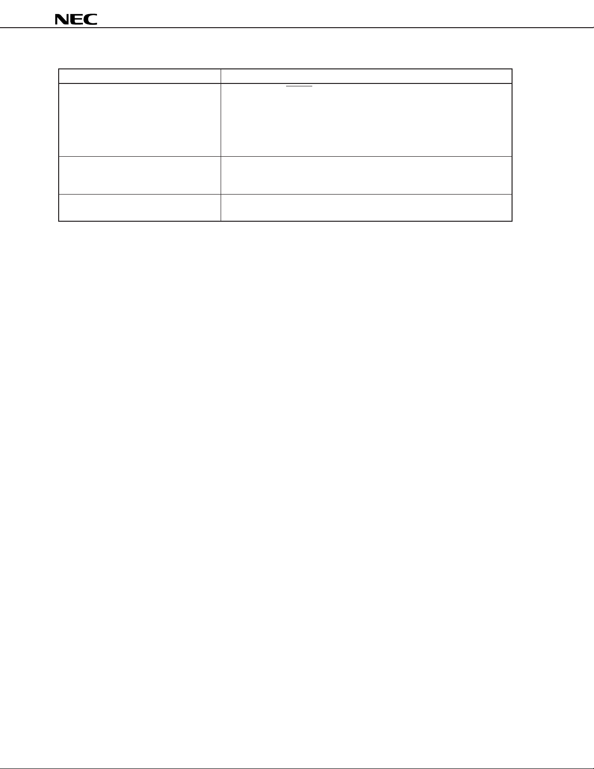
Item Function
Reset • Reset via the RESET pin
• Internal reset by watchdog timer
• Reset by power-ON clear circuit (3-value detection)
• Detection of less than 4.5 V
• Detection of less than 3.5 V
• Detection of less than 2.5 V
Power supply voltage • VDD = 4.5 to 5.5 V (with PLL operating)
•VDD = 3.5 to 5.5 V (with CPU operating, CPU clock: fX/2 or less)
•VDD = 4.5 to 5.5 V (with CPU operating, CPU clock: fX)
Package • 80-pin plastic QFP (14 × 14 mm, 0.65-mm pitch)
• 80-pin ceramic WQFN (14 × 14 mm, 0.65-mm pitch)
Note
(CPU clock: fX)
Note
(CPU clock: fX/2 or less and on power application)
Note
(in STOP mode)
Note These voltage values are maximum values. The reset is actually executed at a voltage lower than these
values.
(2/2)
4
Page 5
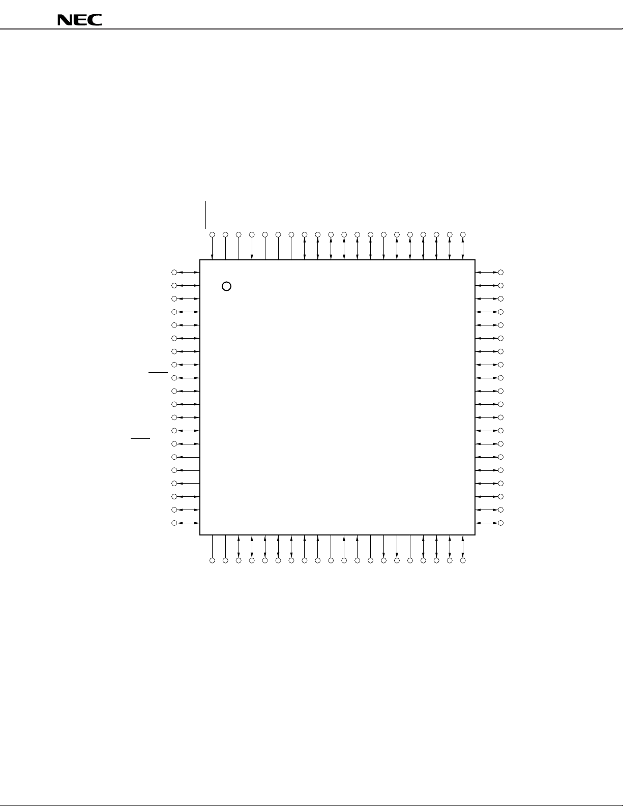
PIN CONFIGURATIONS (TOP VIEW)
(1) Normal operating mode
• 80-PIN PLASTIC QFP (14 × 14 mm, 0.65-mm pitch)
µ
PD178P018GC-3B9
• 80-PIN CERAMIC WQFN (14 × 14 mm, 0.65-mm pitch)
µ
PD178P018KK-T
RESET
P10/ANI0
P11/ANI1
P12/ANI2
P13/ANI3
P14/ANI4
P15/ANI5
P20/SI1
P21/SO1
P22/SCK1
P23/STB
P24/BUSY
P25/SI0/SB0/SDA0
P26/SO0/SB1/SDA1
P27/SCK0/SCL
P132/PWM0
P133/PWM1
P134/PWM2
P40
P41
P42
VDDREGOSCX1X2
80 79 78 77 76 75 74 73 72 71 70 69 68 67 66 65 64 63 62 61
1
2
3
4
5
6
7
8
9
10
11
12
13
14
15
16
17
18
19
20
2122 23 24 25 26 27 28 29 30 31 32 33 34 35 36 37 38 39 40
GND
REGCPU
P06/INTP6
P05/INTP5
P04/INTP4
P03/INTP3
P02/INTP2
P01/INTP1
P00/INTP0
P125
P124
P123
P122
P121
µ
PD178P018
P120
60
59
58
57
56
55
54
53
52
51
50
49
48
47
46
45
44
43
42
41
P37
P36/BEEP
P35
P34/TI2
P33/TI1
P32
P31
P30
P67
P66
P65
P64
P63
P62
P61
P60
P57
P56
P55
P54
GNDPORT
Cautions 1. Connect the V
2. Connect the VDDPORT and VDDPLL pins to VDD.
3. Connect the GNDPORT and GNDPLL pins to GND.
4. Connect each of the REGOSC and REGCPU pins to GND via a 0.1-µF capacitor.
P43
P44
P45
P46
P47
DDPORT
V
PP pin to GND directly.
AMIFC
DDPLL
FMIFC
V
VCOL
VCOH
EO0
GNDPLL
EO1
PP
V
P50
P51
P52
P53
5
Page 6

µ
PD178P018
AMIFC : AM Intermediate Frequency Counter Input
ANI0 to ANI5 : A/D Converter Input
BEEP : Buzzer Output
BUSY : Busy Output
EO0, EO1 : Error Out Output
FMIFC : FM Intermediate Frequency Counter Input
GND : Ground
GNDPLL : PLL Ground
GNDPORT : Port Ground
INTP0 to INTP6 : Interrupt Inputs
P00 to P06 : Port 0
P10 to P15 : Port 1
P20 to P27 : Port 2
P30 to P37 : Port 3
P40 to P47 : Port 4
P50 to P57 : Port 5
P60 to P67 : Port 6
P120 to P125 : Port 12
P132 to P134 : Port 13
PWM0 to PWM2 : PWM Output
REGCPU : Regulator for CPU Power Supply
REGOSC : Regulator for Oscillator
RESET : Reset Input
SB0, SB1 : Serial Data Bus Input/Output
SCK0, SCK1 : Serial Clock Input/Output
SCL : Serial Clock Input/Output
SDA0, SDA1 : Serial Data Input/Output
SI0, SI1 : Serial Data Input
SO0, SO1 : Serial Data Output
STB : Strobe Output
TI1, TI2 : Timer Clock Input
VCOL, VCOH : Local Oscillation Input
DD : Power Supply
V
V
DDPLL : PLL Power Supply
DDPORT : Port Power Supply
V
V
PP : Programming Power Supply
X1, X2 : Crystal Resonator Connection
6
Page 7
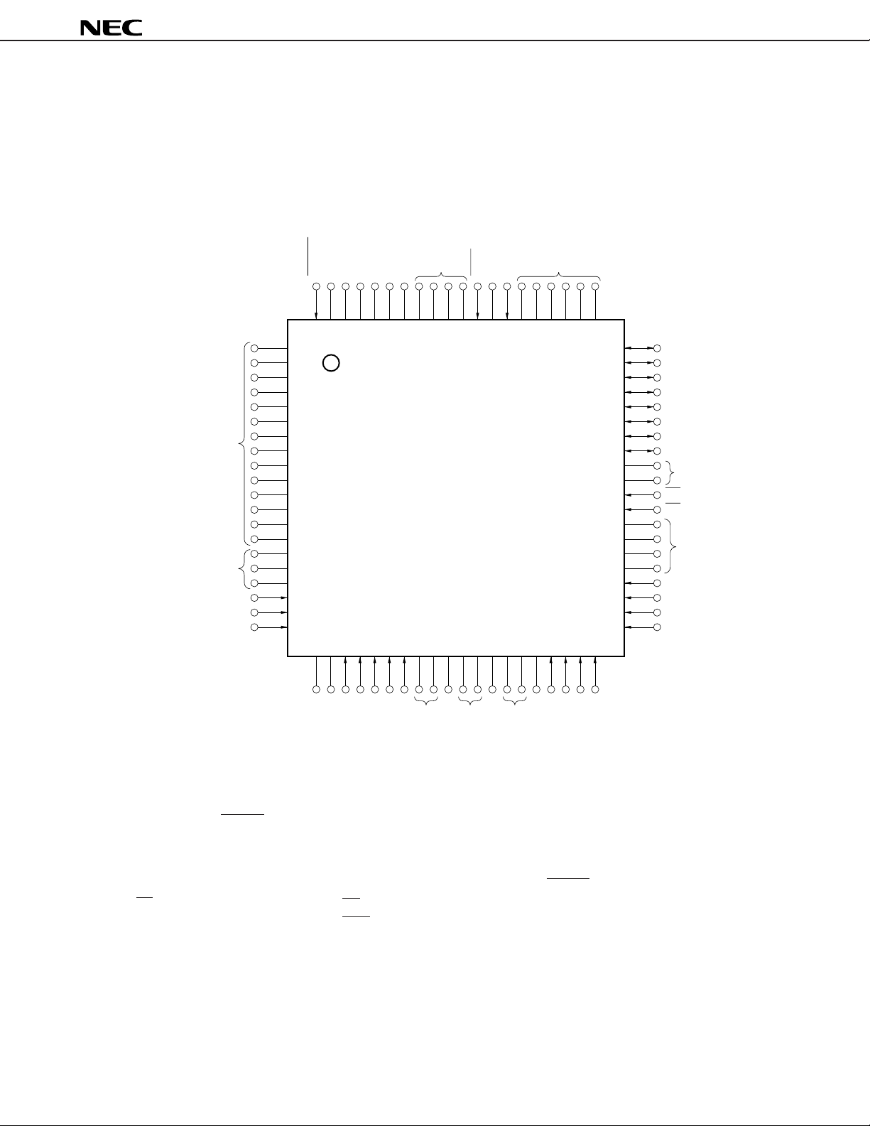
(2) PROM programming mode
µ
PD178P018
• 80-PIN PLASTIC QFP (14 ×
µ
PD178P018GC-3B9
• 80-PIN CERAMIC WQFN
(L)
A0
A1
A2
Note
1
2
3
4
5
6
7
8
9
10
11
12
13
14
15
16
17
18
19
20
µ
PD178P018KK-T
Open
14 mm)
(L)
RESET
VDDVDD(L)
80 79 78 77767574 73 72717069 68 67 66656463 62 61
21 22 23 24252627 28 29303132 33 34 35363738 39 40
Open
GND
DD
V
PGM
(L)
A9
(L)
60
59
58
57
56
55
54
53
52
51
50
49
48
47
46
45
44
43
42
41
D7
D6
D5
D4
D3
D2
D1
D0
(L)
CE
OE
(L)
A15
A14
A13
A12
Open
PP
A8
V
A16
A10
A11
DD
A3A4A5A6A7
V
GND
(L)
DD
V
(L)
GND
Note Under planning
Cautions 1. (L) : Individually connect to GND via a pull-down resistor.
2. GND : Connect to GND.
3. RESET : Set to the low level.
4. Open : Leave open.
A0 to A16 : Address Bus
CE : Chip Enable
D0 to D7 : Data Bus
GND : Ground
OE : Output Enable
PGM : Program
RESET : Reset
V
DD : Power Supply
PP : Programming Power Supply
V
7
Page 8
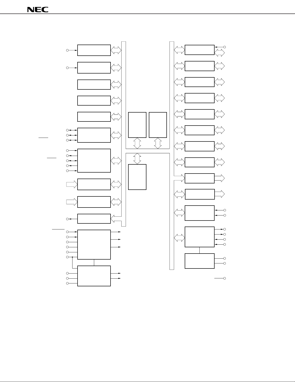
BLOCK DIAGRAM
µ
PD178P018
TI1/P33
TI2/P34
SI0/SB0/SDA0/P25
SO0/SB1/SDA1/P26
SCK0/SCL/P27
SI1/P20
SO1/P21
SCK1/P22
STB/P23
BUSY/P24
ANI0/P10 to
ANI5/P15
INTP0/P00 to
INTP6/P06
BEEP/P36
8-bit TIMER/
EVENT COUNTER 1
8-bit TIMER/
EVENT COUNTER 2
8-bit TIMER3
WATCHDOG TIMER
BASIC TIMER
SERIAL
INTERFACE 0
SERIAL
INTERFACE 1
A/D CONVERTER
6
INTERRUPT
7
CONTROL
BUZZER OUTPUT
78K/0
CPU
CORE
RAM
(3072 Bytes)
PROM
(60 K Bytes)
PORT 0
PORT 1
PORT 2
PORT 3
PORT 4
PORT 5
PORT 6
PORT 12
PORT 13
D/A CONVERTER
(PWM)
FREQUENCY
COUNTER
P00
6
P01 to P06
6
P10 to P15
P20 to P27
8
8
P30 to P37
8
P40 to P47
8
P50 to P57
8
P60 to P67
6
P120 to P125
3
P132 to P134
PWM0/P132 to
3
PWM2/P134
AMIFC
FMIFC
RESET
V
DD
X1
X2
PORT
SYSTEM
CONTROL
RESET
CPU
PERIPHERAL
PLL
EO0
EO1
VCOL
VCOH
GNDPORT
V
REGOSC
REGCPU
DD
V
VOLTAGE
REGULATOR
OSC
V
CPU
PLL
VOLTAGE
REGULATOR
V
DD
PLL
GNDPLL
PP
V
GND
8
Page 9

µ
PD178P018
CONTENTS
1. PIN FUNCTION LIST.......................................................................................................................... 10
1.1 Pins in Normal Operating Mode ............................................................................................... 10
1.2 Pins in PROM Programming Mode........................................................................................... 12
1.3 Pins Input/Output Circuits and Recommended Connection of Unused Pins ...................... 13
2. PROM PROGRAMMING ..................................................................................................................... 16
2.1 Operating Modes........................................................................................................................ 16
2.2 PROM Write Procedure ............................................................................................................. 18
2.3 PROM Read Procedure.............................................................................................................. 22
3. PROGRAM ERASURE (µPD178P018KK-T ONLY) ....................................................................... 23
4. OPAQUE FILM ON ERASURE WINDOW (µPD178P018KK-T ONLY)........................................ 23
5. ONE-TIME PROM VERSION SCREENING .................................................................................... 23
6. ELECTRICAL SPECIFICATIONS ...................................................................................................... 24
7. PACKAGE DRAWINGS ..................................................................................................................... 46
8. RECOMMENDED SOLDERING CONDITIONS ................................................................................. 48
APPENDIX A. DEVELOPMENT TOOLS ................................................................................................ 49
APPENDIX B. RELATED DOCUMENTS ................................................................................................ 53
9
Page 10
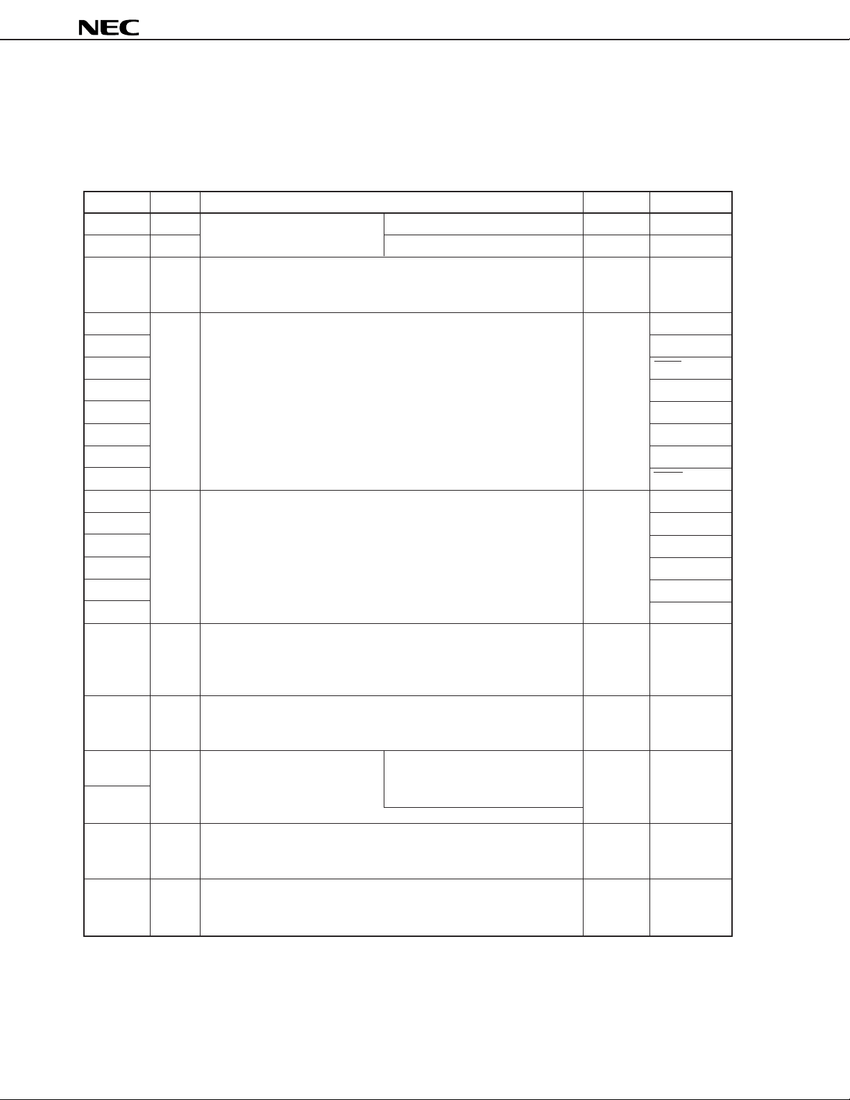
1. PIN FUNCTION LIST
1.1 Pins in Normal Operating Mode
(1) Port pins
µ
PD178P018
Pin Name I/O Function After Reset
P00 Input Port 0. Input only Input INTP0
P01 to P06 I/O 7-bit input/output port.
P10 to P15 I/O Port 1. Input ANI0 to ANI5
6-bit input/output port.
Input/output mode can be specified bit-wise.
P20 I/O Port 2. Input SI1
P21 8-bit input/output port. SO1
P22 Input/output mode can be specified bit-wise. SCK1
P23 STB
P24 BUSY
P25 SI0/SB0/SDA0
P26
P27 SCK0/SCL
P30 to P32 I/O Port 3. Input —
P33 8-bit input/output port. TI1
P34 Input/output mode can be specified bit-wise. TI2
P35 —
P36 BEEP
P37 —
P40 to P47 I/O Port 4. Input —
8-bit input/output port.
Input/output mode can be specified in 8-bit units.
Test input flag (KRIF) is set to 1 by falling edge detection.
P50 to P57 I/O Port 5. Input —
8-bit input/output port.
Input/output mode can be specified bit-wise.
P60 to P63 I/O Port 6. Middle voltage N-ch open-drain Input —
8-bit input/output port. input/output port.
P64 to P67 Input/output mode can be LEDs can be driven directly.
specified bit-wise.
P120 to I/O Port 12. Input —
P125 6-bit input/output port.
Input/output mode can be specified bit-wise.
P132 to Output Port 13. — PWM0 to
P134 3-bit output port. PWM2
N-ch open-drain output port.
Input/output mode can be specified bit-wise.
Input INTP1 to INTP6
Alternate Function
SO0/SB1/SDA1
10
Page 11
(2) Non-port pins (1 of 2)
µ
PD178P018
Pin Name I/O Function After Reset
INTP0 to Input External maskable interrupt inputs with specifiable valid edges (rising Input P00 to P06
INTP6 edge, falling edge, both rising and falling edges).
SI0 Input Serial interface serial data input Input
SI1 P20
SO0 Output Serial interface serial data output Input
SO1 P21
SB0 I/O Serial interface serial data input/output Input P25/SI0/SDA0
SB1
SDA0 P25/SI0/SB0
SDA1 P26/SO0/SB1
SCK0 I/O Serial interface serial clock input/output Input P27/SCL
SCK1 P22
SCL P27/SCK0
STB Output Serial interface automatic transmit/receive strobe output Input P23
BUSY Input Serial interface automatic transmit busy input Input P24
TI1 Input External count clock input to 8-bit timer (TM1) Input P33
TI2 External count clock input to 8-bit timer (TM2) P34
BEEP Output Buzzer output Input P36
ANI0 to ANI5
PWM0 to Output PWM output — P132 to P134
PWM2
EO0, EO1 Output Error out output from charge pump of the PLL frequency synthesizer — —
VCOL Input Inputs PLL local band oscillation frequency (In HF, MF mode). — —
VCOH Input Inputs PLL local band oscillation frequency (In VHF mode). — —
AMIFC Input Inputs AM intermediate frequency counter. — —
FMIFC Input Inputs FM intermediate frequency counter. — —
RESET Input System reset input — —
X1 Input Crystal resonator connection for system clock oscillation — —
X2 — ——
REGOSC — Regulator for oscillator. Connected to GND via a 0.1-µF capacitor. — —
REGCPU — Regulator for CPU power supply. Connected to GND via a 0.1-µF capacitor. — —
VDD — Positive power supply — —
GND — Ground ——
VDDPORT — Positive power supply for port block — —
GNDPORT — Ground for port block — —
VDDPLL — Positive power supply for PLL — —
GNDPLL — Ground for PLL — —
Input A/D converter analog input Input P10 to P15
Alternate Function
P25/SB0/SDA0
P26/SB1/SDA1
P26/SO0/SDA1
11
Page 12
(2) Non-port pins (2/2)
µ
PD178P018
Pin Name I/O Function After Reset
VPP — High-voltage applied during program write/verification. — —
Connected directly to GND in normal operating mode.
Alternate Function
1.2 Pins in PROM Programming Mode
Pin Name I/O Function
RESET Input PROM programming mode setting
When +5 V or +12.5 V is applied to VPP pin and a low-level signal is applied to the RESET pin, this
chip is set in the PROM programming mode.
VPP Input PROM programming mode setting and high-voltage applied during program write/verification.
A0 to A16 Input Address bus
D0 to D7 I/O Data bus
CE Input PROM enable input/program pulse input
OE Input Read strobe input to PROM
PGM Input Program/program inhibit input in PROM programming mode.
VDD — Positive power supply
GND — Ground potential
12
Page 13
µ
PD178P018
1.3 Pins Input/Output Circuits and Recommended Connection of Unused Pins
Table 1-1 shows the input/output circuit types of pins and the recommended conditions for unused pins.
Refer to Figure 1-1 for the configuration of the input/output circuit of each type.
Table 1-1. Type of I/O Circuit of Each Pin
Pin Name I/O Circuit Type I/O Recommended Connections of Unused Pins
P00/INTP0 2 Input Connected to GND or GNDPORT
P01/INTP1 to P06/INTP6 8 I/O Set in general-purpose input port mode by software and
P10/ANI0 to P15/ANI5 11-A individually connected to VDD, VDDPORT, GND, or GNDPORT
P20/SI1 8 via a resistor.
P21/SO1 5
P22/SCK1 8
P23/STB 5
P24/BUSY 8
P25/SI0/SB0/SDA0 10
P26/SO0/SB1/SDA1
P27/SCK0/SCL
P30 to P32 5
P33/TI1, P34/TI2 8
P35 5
P36/BEEP
P37
P40 to P47 5-G
P50 to P57 5
P60 to P63 13
P64 to P67 5
P120 to P125
P132/PWM0 to P134/PWM2 19 Output Set to the low-level output by software and open
EO0 DTS-EO1 Open
EO1 DTS-EO2
VCOL, VCOH DTS-AMP Input Set to disabled status by software and open
AMIFC, FMIFC
VPP — — Connected to GND or GNDPORT directly
13
Page 14
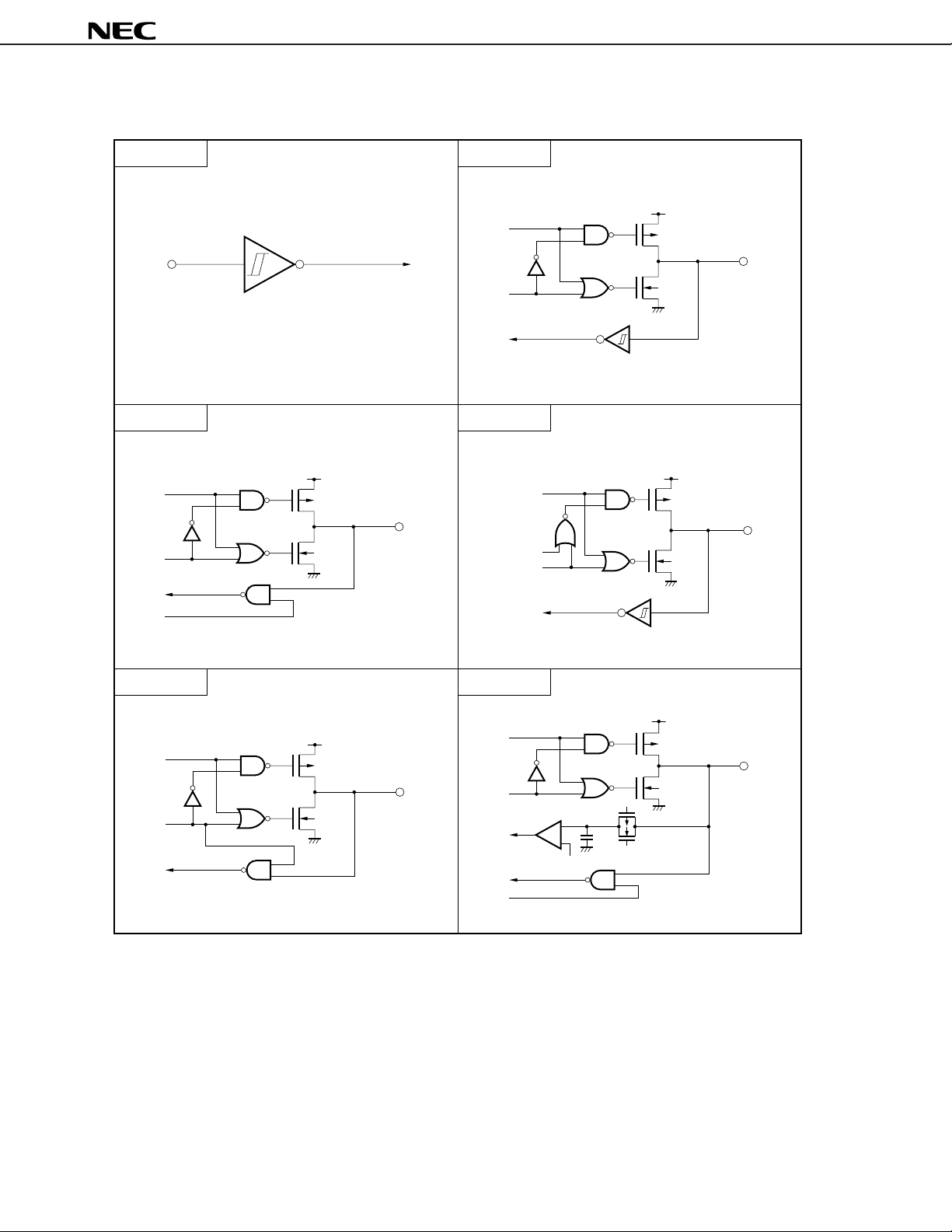
Figure 1-1. Types of Pin Input/Output Circuits (1/2)
Type 2 Type 8
data
IN
output
disable
Schmitt-Triggered Input with Hysteresis Characteristics
V
DD
P-ch
N-ch
µ
PD178P018
IN/OUT
Type 5
data
V
DD
P-ch
Type 10
IN/OUT
output
disable
N-ch
open drain
output disable
input
enable
Type 5-G Type 11-A
V
data
output
disable
DD
P-ch
IN/OUT
N-ch
data
output
disable
comparator
input
enable
data
P-ch
+
–
N-ch
V
REF
(Threshold voltage)
V
DD
P-ch
N-ch
V
P-ch
N-ch
IN/OUT
DD
IN/OUT
Remark All V
14
DD and GND in the above figures are the positive power supply and ground potential of the ports,
and should be read as V
DDPORT and GNDPORT, respectively.
Page 15
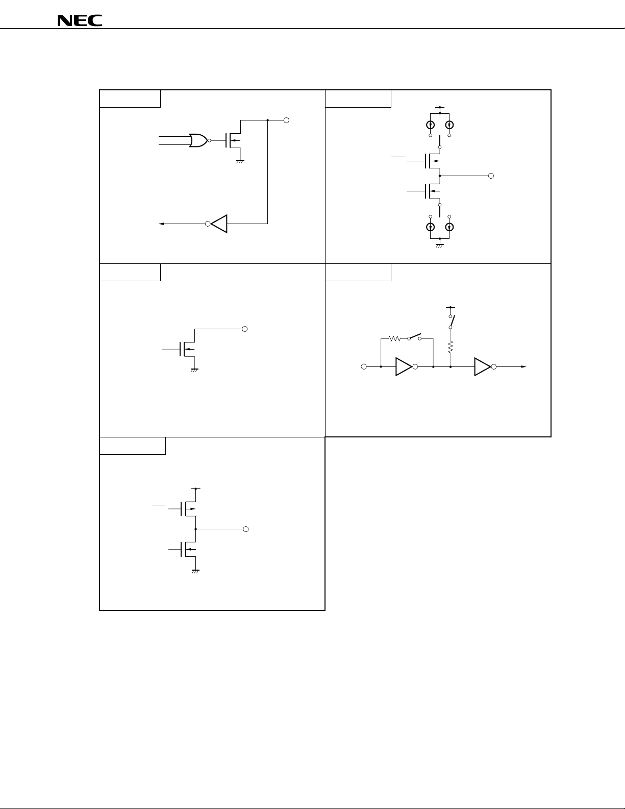
Figure 1-1. Types of Pin Input/Output Circuits (2/2)
µ
PD178P018
Type 13 Type DTS-EO2
IN/OUT
output disable
data
Middle-Voltage Input Buffer
Type 19
N-ch
N-ch
Type DTS-AMP
OUT
IN
DW
UP
DD
V
P-ch
N-ch
GNDPLL
V
PLL
DD
OUT
PLL
Type DTS-EO1
DW
Remark All V
and should be read as V
DD
PLL
V
P-ch
OUT
UP
DD and GND in the above figures are the positive power supply and ground potential of the ports,
N-ch
GNDPLL
DDPORT and GNDPORT, respectively.
15
Page 16
µ
PD178P018
2. PROM PROGRAMMING
The µPD178P018 has an internal 60-Kbyte PROM as a program memory. For programming, set the PROM
programming mode with the V
PP and RESET pins. For the connection of unused pins, refer to “PIN CONFIGURA-
TIONS (TOP VIEW) (2) PROM programming mode.”
Caution Programs must be written in addresses 0000H to EFFFH (the last address EFFFH must be
specified). They cannot be written by a PROM writer which cannot specify the write address.
2.1 Operating Modes
When +5 V or +12.5 V is applied to the V
PP pin and a low-level signal is applied to the RESET pin, the PROM
programming mode is set. This mode will become the operating mode as shown in Table 2-1 when the CE, OE, and
PGM pins are set as shown.
Further, when the read mode is set, it is possible to read the contents of the PROM.
Table 2-1. Operating Modes of PROM Programming
Pin RESET VPP VDD CE OE PGM D0 to D7
Operating Mode
Page data latch L +12.5 V +6.5 V H L H Data input
Page write H H L High-impedance
Byte write L H L Data input
Program verify L L H Data output
Program inhibit x H H High-impedance
xLL
Read +5 V +5 V L L H Data output
Output disable L H x High-impedance
Standby H x x High-impedance
Remark x : L or H
16
Page 17

µ
PD178P018
(1) Read mode
Read mode is set if CE = L and OE = L are set.
(2) Output disable mode
Data output becomes high-impedance, and is in the output disable mode, if OE = H is set.
µ
Therefore, it allows data to be read from any device by controlling the OE pin, if multiple
connected to the data bus.
(3) Standby mode
Standby mode is set if CE = H is set.
In this mode, data outputs become high-impedance irrespective of the OE status.
(4) Page data latch mode
Page data latch mode is set if CE = H, PGM = H, and OE = L are set at the beginning of page write mode.
In this mode, 1 page 4-byte data is latched in an internal address/data latch circuit.
(5) Page write mode
After 1 page 4 bytes of addresses and data are latched in the page data latch mode, a page write is executed
by applying a 0.1-ms program pulse (active low) to the PGM pin with CE = H and OE = H. Then, program
verification can be performed, if CE = L and OE = L are set.
If programming is not performed by a one-time program pulse, X times (X ≤ 10) write and verification operations
should be executed repeatedly.
PD178P018s are
(6) Byte write mode
Byte write is executed when a 0.1-ms program pulse (active low) is applied to the PGM pin with CE = L and OE
= H. Then, program verification can be performed if OE = L is set.
If programming is not performed by a one-time program pulse, X times (X ≤ 10) write and verification operations
should be executed repeatedly.
(7) Program verify mode
Program verify mode is set if CE = L, PGM = H, and OE = L are set.
In this mode, check if a write operation is performed correctly after the write.
(8) Program inhibit mode
Program inhibit mode is used when the OE pin, V
in parallel and a write is performed to one of those devices.
When a write operation is performed, the page write mode or byte write mode described above is used. At this
time, a write is not performed to a device which has the PGM pin driven high.
PP pin, and D0 to D7 pins of multiple
µ
PD178P018s are connected
17
Page 18
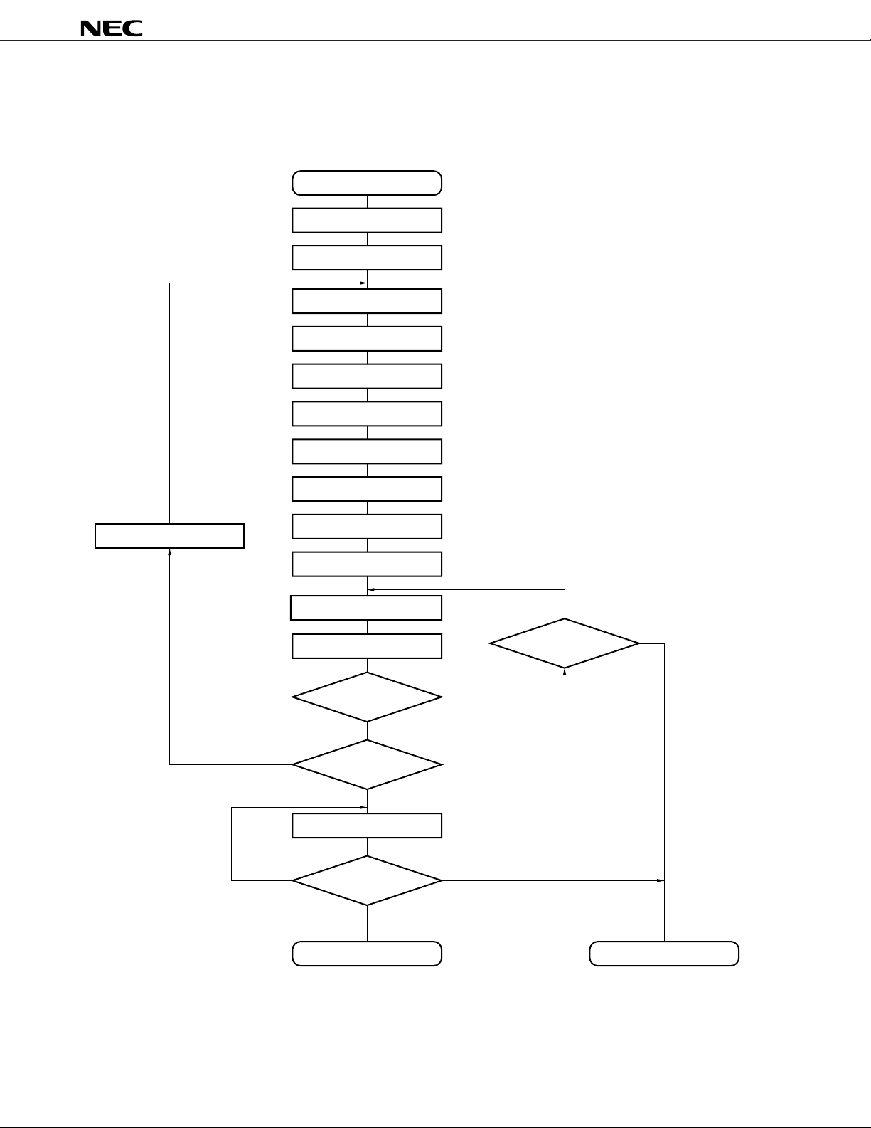
2.2 PROM Write Procedure
Figure 2-1. Page Program Mode Flow Chart
Start
Address = G
DD
= 6.5 V, V
V
Address = Address + 1
X = 0
Latch
Latch
PP
= 12.5 V
µ
PD178P018
Address = Address + 1
Address = Address + 1
Address = Address + 1
0.1-ms program pulse
No
Address = N?
V
DD
= 4.5 to 5.5 V, V
Latch
Latch
X = X + 1
Verify
4 bytes
Pass
Yes
PP
= V
No
X = 10?
Fail
DD
Yes
Remark G = Start address
N = Program last address
18
Pass
Verify
all bytes
All Pass
Write end Defective product
Fail
Page 19

A2 to A16
A0, A1
D0 to D7
V
V
PP
V
µ
PD178P018
Figure 2-2. Page Program Mode Timing
Page Data Latch Program VerifyPage Program
Data Input Data Output
PP
DD
V
CE
PGM
OE
VDD + 1.5
DD
V
V
V
V
DD
IH
V
IL
IH
V
IL
IH
V
IL
19
Page 20

Figure 2-3. Byte Program Mode Flow Chart
Start
Address = G
DD
V
= 6.5 V, V
X = 0
PP
= 12.5 V
µ
PD178P018
Address = Address + 1
Remark G = Start address
N = Program last address
No
Pass
X = X + 1
0.1-ms program pulse
Vefity
Pass
Address = N?
Yes
DD
= 4.5 to 5.5 V, V
V
Verify
all bytes
All Pass
Write end Defective product
PP
= V
No
X = 10?
Fail
DD
Fail
Yes
20
Page 21

Figure 2-4. Byte Program Mode Timing
Program Program Verify
A0 to A16
D0 to D7 Data Input Data Output
V
PP
PP
V
V
DD
VDD + 1.5
V
DD
V
DD
µ
PD178P018
V
IH
CE
V
IL
IH
V
PGM
V
IL
IH
V
OE
V
IL
Cautions 1. VDD should be applied before VPP, and removed after VPP.
2. V
PP must not exceed +13.5 V including overshoot.
3. Reliability may be adversely affected if removal/reinsertion is performed while +12.5 V is being
applied to VPP.
21
Page 22

µ
PD178P018
2.3 PROM Read Procedure
The contents of PROM are readable to the external data bus (D0 to D7) according to the read procedure shown
below.
(1) Fix the RESET pin at low level, supply +5 V to the V
“PIN CONFIGURATIONS (TOP VIEW) (2) PROM programming mode”.
(2) Supply +5 V to the V
(3) Input address of read data into the A0 to A16 pins.
(4) Read mode
(5) Output data to D0 to D7 pins.
The timings of the above steps (2) to (5) are shown in Figure 2-5.
DD and VPP pins.
PP pin, and connect all other unused pins as shown in
Figure 2-5. PROM Read Timings
Address InputA0 to A16
CE (Input)
OE (Input)
Hi-Z Hi-Z
Data OutputD0 to D7
22
Page 23

µ
PD178P018
3. PROGRAM ERASURE (µPD178P018KK-T ONLY)
The µPD178P018KK-T is capable of erasing (FFH) the data written in a program memory and rewriting.
To erase the programmed data, expose the erasure window to light having a wavelength shorter than about 400
nm. Normally, irradiate ultraviolet rays of 254-nm wavelength. The amount of exposure required to completely erase
the programmed data is as follows:
2
• UV intensity x erasure time: 30 W•s/cm
• Erasure time: 40 min. or more (When a UV lamp of 12,000
needed because of deterioration in performance of the UV lamp, soiled erasure window, etc.)
When erasing the contents of the data, set up the UV lamp within 2.5 cm from the erasure window. Further, if a
filter is provided for a UV lamp, irradiate the ultraviolet rays after removing the filter.
or more
µ
W/cm2 is used. However, a longer time may be
4. OPAQUE FILM ON ERASURE WINDOW (µPD178P018KK-T ONLY)
To protect from an intentional erasure by rays other than that of the lamp for erasing EPROM contents, or to protect
internal circuit other than EPROM from misoperating by rays, cover the erasure window with an opaque film when
EPROM contents erasure is not performed.
5. ONE-TIME PROM VERSION SCREENING
The one-time PROM version (µPD178P018GC-3B9) cannot be tested completely by NEC before it is shipped,
because of its structure. It is recommended to perform screening to verify PROM after writing necessary data and
performing high-temperature storage under the condition below.
Storage Temperature Storage Time
125°C 24 hours
23
Page 24

µ
PD178P018
6. ELECTRICAL SPECIFICATIONS
ABSOLUTE MAXIMUM RATINGS (TA = 25°C)
Parameter Symbol Test Conditions Ratings Unit
Power supply voltage VDD –0.3 to +7.0 V
VPP –0.3 to +13.5 V
Input voltage VI1 Excluding P60 to P63 –0.3 to VDD + 0.3 V
VI2 P60 to P63 N-ch open-drain –0.3 to +16 V
VI3 A9 PROM programming mode –0.3 to +13.5 V
Output voltage VO –0.3 to VDD + 0.3 V
Output withstand VBDS P132 to P134 N-ch open-drain 16 V
voltage
Analog input voltage
Output current high IOH 1 pin –10 mA
Output current low IOL
Operating ambient TA –40 to +85 °C
temperature
Storage temperature T stg –65 to +150 °C
VAN P10 to P15 Analog input pin –0.3 to VDD + 0.3 V
P01 to P06, P30 to P37, P56, P57, P60 to P67, –15 mA
P120 to P125 total
P10 to P15, P20 to P27, P40 to P47, P50 to P55, –15 mA
P132 to P134 total
Note
1 pin Peak value 15 mA
r.m.s. value 7.5 mA
Note r.m.s. (root mean square) value should be calculated as follows: [r.m.s value] = [Peak value] × √duty
Caution Product quality may suffer if the absolute maximum rating is exceeded for even a single
parameter even momentarily. That is, the absolute maximum ratings are rated values at which
the product is on the verge of suffering physical damage, and therefore the product must be
used under conditions which ensure that the absolute maximum ratings are not exceeded.
Remark The characteristics of an alternate-function pin and a port pin are the same unless specified otherwise.
RECOMMENDED SUPPLY VOLTAGE RANGES (T
Parameter Symbol Test Conditions MIN. TYP. MAX. Unit
Power supply voltage VDD1 During CPU operation and PLL operation. 4.5 5.5 V
VDD2 While the CPU is operating and the PLL is stopped. 3.5 5.5 V
Cycle Time: TCY ≥ 0.89 µs
VDD3 While the CPU is operating and the PLL is stopped. 4.5 5.5 V
Cycle Time: TCY = 0.44 µs
A = –40 to +85°C)
Remark TCY: Cycle Time (Minimum instruction execution time)
24
Page 25

µ
PD178P018
DC CHARACTERISTICS (TA = –40 to +85°C, VDD = 3.5 to 5.5 V)
Parameter Symbol Test Conditions MIN. TYP. MAX. Unit
Input voltage high VIH1 P10 to P15, P21, P23, 0.7VDD VDD V
P30 to P32, P35 to P37,
P40 to P47, P50 to P57,
P64 to P67, P120 to P125
VIH2 P00 to P06, P20, P22, 0.85VDD VDD V
P24 to P27, P33, P34,
RESET
VIH3 P60 to P63 0.7VDD 15 V
(N-ch open-drain)
Input voltage low VIL1 P10 to P15, P21, P23, 0 0.3VDD V
P30 to P32, P35 to P37,
P40 to P47, P50 to P57,
P64 to P67, P120 to P125
VIL2 P00 to P06, P20, P22, 0 0.15VDD V
P24 to P27, P33, P34,
RESET
VIL3 P60 to P63 4.5 V ≤ VDD ≤ 5.5 V 0 0.3V DD V
(N-ch open-drain) 3.5 V ≤ VDD < 4.5 V 0 0.2VDD V
Output voltage high VOH1 4.5 V ≤ VDD ≤ 5.5 V, VDD – 1.0 V
IOH = –1 mA
3.5 V ≤ VDD < 4.5 V, VDD – 0.5 V
IOH = –100 µA
Output voltage low VOL1 P50 to P57, P60 to P63 VDD = 4.5 to 5.5 V, 0.4 2.0 V
IOH = 15 mA
P01 to P06, P10 to P15, V DD = 4.5 to 5.5 V, 0.4 V
P20 to P27, P30 to P37, I OL = 1.6 mA
P40 to P47, P64 to P67,
P120 to P125,
P132 to P134
VOL2 SB0, SB1, SCK0 VDD = 4.5 to 5.5 V, 0.2VDD V
N-ch open-drain pulled-up
(R = 1 KΩ)
(1/3)
Remark The characteristics of an alternate-function pin and a port pin are the same unless specified otherwise.
25
Page 26

µ
PD178P018
DC CHARACTERISTICS (TA = –40 to +85°C, VDD = 3.5 to 5.5 V)
Parameter Symbol Test Conditions MIN. TYP. MAX. Unit
Input leakage ILIH1 P00 to P06, P10 to P15, VIN = VDD 3
current high P20 to P27, P30 to P37,
P40 to P47, P50 to P57,
P64 to P67, P120 to P125,
RESET
ILIH2 P60 to P63 VIN = 15 V 80
Input leakage ILIL1 P00 to P06, P10 to P15, VIN = 0 V –3
current low P20 to P27, P30 to P37,
P40 to P47, P50 to P57,
P64 to P67, P120 to P125,
RESET
ILIL2 P60 to P63 –3
Output leakage ILOH P132 to P134 VOUT = 15 V 3
current high
Output leakage ILOL P132 to P134 VOUT = 0 V –3
current low
Output off leak ILOF EO0, EO1 VOUT = VDD, ±1
current VOUT = 0 V
Note
Note When an input instruction is executed, the low-level input leakage current for P60 to P63 becomes –200
µ
A (MAX.) only in one clock cycle (at no wait). It remains at –3 µA (MAX.) for other than an input instruction.
(2/3)
µ
A
µ
A
µ
A
µ
A
µ
A
µ
A
µ
A
Remark The characteristics of an alternate-function pin and a port pin are the same unless specified otherwise.
REFERENCE CHARACTERISTICS (TA = 25°C, VDD = 5 V)
Parameter Symbol Test Conditions MIN. TYP. MAX. Unit
Output current high IOH1 EO0 VOUT = VDD – 1 V –4 mA
EO1 (EOCON0 = 1) –6 mA
EO1 (EOCON0 = 0) –2 mA
Output current low IOL1 EO0 VOUT = 1 V 6 mA
EO1 (EOCON0 = 1) 8 mA
EO1 (EOCON0 = 0) 3 mA
(1/2)
26
Page 27

µ
PD178P018
DC CHARACTERISTICS (TA = –40 to +85°C, VDD = 3.5 to 5.5 V)
Parameter Symbol Test Conditions MIN. TYP. MAX. Unit
Power supply IDD1 While the CPU is operating TCY = 0.89 µs
Note 1
current
IDD2
IDD3 While the CPU is operating TCY = 0.89 µs
IDD4 Pin X1 sine wave TCY = 0.44 µs
Data hold VDDR1 When the crystal is oscillating TCY = 0.44 µs 4.5 5.5 V
power supply
voltage
Data hold
power supply current
VDDR2 TCY = 0.89 µs 3.5 5.5 V
VDDR3 When the crystal oscillation is stopped 2.7 5.5 V
IDDR1 While the crystal oscillation TA = 25°C, VDD = 5V 2 4
IDDR2
and the PLL is stopped
fX = 4.5-MHz operation
and the PLL is stopped
HALT Mode.
input VIN = VDD VDD = 4.5 to 5.5 V
fX = 4.5-MHz operation
When power off by Power On Clear is detected
is stopped
TCY = 0.44 µs
VDD = 4.5 to 5.5 V
Note 2
Note 3
Note 2
Note 3
2.5 15 mA
4.0 27 mA
14mA
1.6 6 mA
230
Notes 1. The port current is not included.
2. When the Processor Clock Control register (PCC) is set at 00H, and the Oscillation Mode Select
register (OSMS) is set to 00H.
3. When PCC is set to 00H and OSMS is set to 01H.
(3/3)
µ
A
µ
A
Remarks 1. T
CY: Cycle Time (Minimum instruction execution time)
2. fx: System clock oscillation frequency.
REFERENCE CHARACTERISTICS (T
Parameter Symbol Test Conditions MIN. TYP. MAX. Unit
Power supply IDD5 During CPU operation TCY = 0.44 µs
current and PLL operation.
VCOH pin sine wave
input
fIN = 130 MHz,
VIN = 0.15 Vp-p
A = 25°C, VDD = 5 V)
Note
7mA
Note When the Processor Clock Control register (PCC) is set to 00H, and the Oscillation Mode Select register
(OSMS) is set to 01H.
Remark T
CY: Cycle Time (Minimum instruction execution time)
(2/2)
27
Page 28

AC CHARACTERISTICS
µ
PD178P018
(1) BASIC OPERATION (T
Parameter Symbol Test Conditions MIN. TYP. MAX. Unit
Cycle time TCY fXX = fX/2
(Minimum instruction
execution time)
TI1, TI2 input fTI 4.5 ≤ VDD ≤ 5.5 V 0 4.5 MHz
frequency
TI1, TI2 input high/ tTIH, 4.5 ≤ VDD ≤ 5.5 V 111 ns
low-level width
Interrupt input high/ TINTH, INTP0 8/fsam
low-level width
RESET low-level tRSL 10
width
tTIL 3.5 V ≤ VDD < 4.5 V 1.8
TINTL INTP1 to INTP6 10
A = –40 to +85°C, VDD = 3.5 to 5.5 V)
Note 1
, fX = 4.5-MHz operation 0.89 14.22
Note 2
fXX = fX
fX = 4.5-MHz operation
3.5 V ≤ VDD < 4.5 V 0 275 kHz
, 4.5 ≤ VDD ≤ 5.5 V 0.44 7.11
3.5 ≤ VDD < 4.5 V 0.89 7.11
Note 3
Notes 1. When the Oscillation Mode Selection register (OSMS) is set to 00H.
2. When OSMS is set to 01H.
3. In combination with bits 0 (SCS0) and 1 (SCS1) of the Sampling Clock Select register (SCS),
selection of f
Remarks 1. f
2. f
sam is possible among fXX/2
XX: System clock frequency (fX or fX/2)
X: System clock oscillation frequency
N
, fXX/32, fXX/64, and fXX/128 (when N = 0 to 4).
µ
s
µ
s
µ
s
µ
s
µ
s
µ
s
µ
s
T
CY vs VDD
(when system clock fXX is operating at fX/2)
60
10
s]
µ
CY [
2.0
1.0
Cycle Time T
0.5
0.4
0
123456
Power Supply Voltage VDD [V] Power Supply Voltage VDD [V]
Operation
Guaranteed
Range
T
CY vs VDD
(when system clock fXX is operating at fX)
60
10
s]
µ
Operation
2.0
1.0
Cycle Time TCY [
0.5
0.4
0
123456
Guaranteed
Range
28
Page 29

µ
PD178P018
(2) SERIAL INTERFACE (TA = –40 to +85°C, VDD = 3.5 to 5.5 V)
(a) Serial interface channel 0
(i) 3-wire serial I/O mode (SCK0 ... internal clock output)
Parameter Symbol Test Conditions MIN. TYP. MAX. Unit
SCK0 cycle time tKCY1 4.5 V ≤ VDD ≤ 5.5 V 800 ns
3.5 V ≤ VDD < 4.5 V 1600 ns
SCK0 high-/low-level width tKH1, 4.5 V ≤ VDD ≤ 5.5 V
tKL1 3.5 V ≤ VDD < 4.5 V
SI0 setup time (to SCK0↑)tSIK1 4.5 V ≤ VDD ≤ 5.5 V 100 ns
3.5 V ≤ VDD < 4.5 V 150 ns
SI0 hold time (from SCK0↑)tKSI1 400 ns
SO0 output delay time from SCK0↓ tKSO1 C = 100 pF
Note
tKCY1/2 – 50
tKCY1/2 – 100
ns
ns
300 ns
Note C is the load capacitance of the SO0 output line.
(ii) 3-wire serial I/O mode (SCK0 ... external clock input)
Parameter Symbol Test Conditions MIN. TYP. MAX. Unit
SCK0 cycle time tKCY2 4.5 V ≤ VDD ≤ 5.5 V 800 ns
3.5 V ≤ VDD < 4.5 V 1600 ns
SCK0 high-/low-level width tKH2, 4.5 V ≤ VDD ≤ 5.5 V 400 ns
tKL2 3.5 V ≤ VDD < 4.5 V 800 ns
SI0 setup time (to SCK0↑)tSIK2 100 ns
SI0 hold time (from SCK0↑)tKSI2 400 ns
SO0 output delay time from SCK0↓ tKSO2 C = 100 pF
Note
300 ns
SCK0 rising or falling edge time tR2, tF2 1000 ns
Note C is the load capacitance of the SO0 output line.
29
Page 30

µ
PD178P018
(iii) SBI mode (SCK0 ... internal clock output)
Parameter Symbol Test Conditions MIN. TYP. MAX. Unit
SCK0 cycle time tKCY3 4.5 V ≤ VDD ≤ 5.5 V 800 ns
3.5 V ≤ VDD < 4.5 V 3200 ns
SCK0 high-/low-level width tKH3, 4.5 V ≤ VDD ≤ 5.5 V
tKL3 3.5 V ≤ VDD < 4.5 V
SB0, SB1 setup time (to SCK0↑)tSIK3 4.5 V ≤ VDD ≤ 5.5 V 100 ns
3.5 V ≤ VDD < 4.5 V 300 ns
SB0, SB1 hold time (from SCK0↑)
SB0, SB1 output delay time from tKSO3 R = 1 kΩ 4.5 V ≤ VDD ≤ 5.5 V 0 250 ns
SCK0↓
SB0, SB1↓ from SCK0
SCK0↓ from SB0, SB1↓ tSBK tKCY3 ns
SB0, SB1 high-level width tSBH tKCY3 ns
SB0, SB1 low-level width tSBL tKCY3 ns
↑
tKSI3 tKCY3/2 ns
C = 100 pF
tKSB tKCY3 ns
Note
3.5 V ≤ VDD < 4.5 V 0 1000 ns
tKCY3/2 – 50
tKCY3/2 – 150
Note R and C are the load resistance and load capacitance of the SB0 and SB1 output lines.
(iv) SBI mode (SCK0 ... external clock input)
Parameter Symbol Test Conditions MIN. TYP. MAX. Unit
SCK0 cycle time tKCY4 4.5 V ≤ VDD ≤ 5.5 V 800 ns
3.5 V ≤ VDD < 4.5 V 3200 ns
ns
ns
SCK0 high-/low-level width tKH4, 4.5 V ≤ VDD ≤ 5.5 V 400 ns
tKL4 3.5 V ≤ VDD < 4.5 V 1600 ns
SB0, SB1 setup time (to SCK0↑)tSIK4 4.5 V ≤ VDD ≤ 5.5 V 100 ns
3.5 V ≤ VDD < 4.5 V 300 ns
SB0, SB1 hold time (from SCK0↑)
SB0, SB1 output delay time from tKSO4 R = 1 kΩ 4.5 V ≤ VDD ≤ 5.5 V 0 300 ns
SCK0↓
SB0, SB1↓ from SCK0
SCK0↓ from SB0, SB1↓ tSBK tKCY4 ns
SB0, SB1 high-level width tSBH tKCY4 ns
SB0, SB1 low-level width tSBL tKCY4 ns
SCK0 rising or falling edge time tR4, tF4 1000 ns
↑
tKSI4 tKCY4/2 ns
C = 100 pF
tKSB tKCY4 ns
Note
3.5 V ≤ VDD < 4.5 V 0 1000 ns
Note R and C are the load resistance and load capacitance of the SB0 and SB1 output lines.
30
Page 31

µ
PD178P018
(v) 2-wire serial I/O mode (SCK0 ... internal clock output)
Parameter Symbol Test Conditions MIN. TYP. MAX. Unit
SCK0 cycle time tKCY5 R = 1 kΩ 1600 ns
SCK0 high-level width tKH5
C = 100 pF
Note
tKCY5/2 – 160
ns
SCK0 low-level width t KL5 4.5 V ≤ VDD ≤ 5.5 V
3.5 V ≤ VDD < 4.5 V
SB0, SB1 setup time (to SCK0↑)tSIK5 4.5 V ≤ VDD ≤ 5.5 V 300 ns
3.5 V ≤ VDD < 4.5 V 350 ns
SB0, SB1 hold time (from SCK0↑)
SB0, SB1 output delay time from tKSO5 0 300 ns
SCK0↓
tKSI5 600 ns
tKCY5/2 – 50
tKCY5/2 – 100
400 ns
ns
ns
Note R and C are the load resistance and load capacitance of the SCK0, SB0, and SB1 output lines.
(vi) 2-wire serial I/O mode (SCK0 ... external clock input)
Parameter Symbol Test Conditions MIN. TYP. MAX. Unit
SCK0 cycle time tKCY6 1600 ns
SCK0 high-level width tKH6 650 ns
SCK0 low-level width t KL6 800 ns
SB0, SB1 setup time (to SCK0↑)tSIK6 100 ns
SB0, SB1 hold time (from SCK0↑)
SB0, SB1 output delay time from tKSO6 R = 1 kΩ 4.5 V ≤ VDD ≤ 5.5 V 0 300 ns
SCK0↓
tKSI6 tKCY6/2 ns
C = 100 pF
Note
3.5 V ≤ VDD < 4.5 V 0 500 ns
SCK0 at rising or falling edge time tR6, tF6 1000 ns
Note R and C are the load resistance and load capacitance of the SB0 and SB1 output lines.
31
Page 32

µ
PD178P018
(vii) I2C bus mode (SCL ... internal clock output)
Parameter Symbol Test Conditions MIN. TYP. MAX. Unit
SCL cycle time tKCY7 R = 1 kΩ 10
SCL high-level width tKH7
SCL low-level width tKL7 tKCY7 – 50 ns
SDA0, SDA1 setup time (to SCL↑)
SDA0, SDA1 hold time tKSI7 0ns
(from SCL↓)
SDA0, SDA1 output delay time tKSO7 4.5 V ≤ VDD ≤ 5.5 V 0 300 ns
(from SCL↓)
SDA0, SDA1↓ from SCL↑ or tKSB 200 ns
SDA0, SDA1↑ from SCL
SCL↓ from SDA0, SDA1↓ tSBK 400 ns
SDA0, SDA1 high-level width tSBH 500 ns
↑
tSIK7 200 ns
C = 100 pF
Note
3.5 V ≤ VDD < 4.5 V 0 500 ns
tKCY7 – 160
µ
ns
s
Note R and C are the load resistance and load capacitance of the SCL, SDA0, and SDA1 output lines.
(viii) I2C bus mode (SCL ... external clock input)
Parameter Symbol Test Conditions MIN. TYP. MAX. Unit
SCL cycle time tKCY8 1000 ns
SCL high-/low-level width tKH8, tKL8 400 ns
SDA0, SDA1 setup time (to SCL↑)
SDA0, SDA1 hold time tKSI8 0ns
(from SCL↓)
SDA0, SDA1 output delay time tKSO8 R = 1 kΩ 4.5 V ≤ VDD ≤ 5.5 V 0 300 ns
from SCL↓
SDA0, SDA1↓ from SCL↑ or tKSB 200 ns
SDA0, SDA1↑ from SCL↑
SCL↓ from SDA0, SDA1↓ tSBK 400 ns
SDA0, SDA1 high-level width tSBH 500 ns
SCL rising or falling edge time tR8, tF8 1000 ns
tSIK8 200 ns
C = 100 pF
Note
3.5 V ≤ VDD < 4.5 V 0 500 ns
Note R and C are the load resistance and load capacitance of the SDA0 and SDA1 output lines.
32
Page 33

µ
PD178P018
(b) Serial interface channel 1
(i) 3-wire serial I/O mode (SCK1 ... internal clock output)
Parameter Symbol Test Conditions MIN. TYP. MAX. Unit
SCK1 cycle time tKCY9 4.5 V ≤ VDD ≤ 5.5 V 800 ns
3.5 V ≤ VDD < 4.5 V 1600 ns
SCK1 high-/low-level width tKH9, 4.5 V ≤ VDD ≤ 5.5 V
tKL9 3.5 V ≤ VDD < 4.5 V
SI1 setup time (to SCK1↑)tSIK9 4.5 V ≤ VDD ≤ 5.5 V 100 ns
3.5 V ≤ VDD < 4.5 V 150 ns
SI1 hold time (from SCK1↑)tKSI9 400 ns
SO1 output delay time (from SCK1↓)
tKSO9 C = 100 pF
Note
tKCY9/2 – 50
tKCY9/2 – 100
ns
ns
300 ns
Note C is the load capacitance of the SO1 output line.
(ii) 3-wire serial I/O mode (SCK1 ... external clock input)
Parameter Symbol Test Conditions MIN. TYP. MAX. Unit
SCK1 cycle time tKCY10 4.5 V ≤ VDD ≤ 5.5 V 800 ns
3.5 V ≤ VDD < 4.5 V 1600 ns
SCK1 high-/low-level width tKH10, 4.5 V ≤ VDD ≤ 5.5 V 400 ns
tKL10 3.5 V ≤ VDD < 4.5 V 800 ns
SI1 setup time (to SCK1↑)tSIK10 100 ns
SI1 hold time (from SCK1↑)tKSI10 400 ns
SO1 output delay time (from SCK1↓
)tKSO10 C = 100 pF
Note
300 ns
SCK1 rising or falling edge time tR10, tF10 1000 ns
Note C is the load capacitance of the SO1 output line.
33
Page 34

µ
PD178P018
(iii) 3-wire serial I/O mode with automatic transmit/receive function (SCK1 ... internal clock
output)
Parameter Symbol Test Conditions MIN. TYP. MAX. Unit
SCK1 cycle time tKCY11 4.5 V ≤ VDD ≤ 5.5 V 800 ns
3.5 V ≤ VDD < 4.5 V 1600 ns
SCK1 high-/low-level width tKH11, 4.5 V ≤ VDD ≤ 5.5 V
tKL11 3.5 V ≤ VDD < 4.5 V
SI1 setup time (to SCK1↑)tSIK11 4.5 V ≤ VDD ≤ 5.5 V 100 ns
3.5 V ≤ VDD < 4.5 V 150 ns
SI1 hold time (from SCK1↑)tKSI11 400 ns
SO1 output delay time (from SCK1↓
STB↑ from SCK1
Strobe signal high-level width tSBW
Busy signal setup time tBYS 100 ns
(to busy signal detection timing)
Busy signal hold time tBYH 4.5 V ≤ VDD ≤ 5.5 V 100 ns
(from busy signal detection timing)
SCK1↓ from busy inactive tSPS 2tKCY11 ns
↑
)tKSO11 C = 100 pF
tSBD
3.5 V ≤ VDD < 4.5 V 150 ns
Note
tKCY11/2 – 50
tKCY11/2 – 100
300 ns
tKCY11/2 – 100 tKCY11/2 + 100
tKCY11 – 30 tKCY11 + 30
ns
ns
ns
ns
Note C is the load capacitance of the SO1 output line.
(iv) 3-wire serial I/O mode with automatic transmit/receive function (SCK1 ... external clock
input)
Parameter Symbol Test Conditions MIN. TYP. MAX. Unit
SCK1 cycle time tKCY12 4.5 V ≤ VDD ≤ 5.5 V 800 ns
3.5 V ≤ VDD < 4.5 V 1600 ns
SCK1 high-/low-level width tKH12, 4.5 V ≤ VDD ≤ 5.5 V 400 ns
tKL12 3.5 V ≤ VDD < 4.5 V 800 ns
SI1 setup time (to SCK1↑)tSIK12 100 ns
SI1 hold time (from SCK1↑)tKSI12 400 ns
SO1 output delay time (from SCK1↓
SCK1 rising or falling edge time tR12, tF12 1000 ns
)tKSO12 C = 100 pF
Note
300 ns
Note C is the load capacitance of the SO1 output line.
34
Page 35

AC Timing Test Point (Excluding X1 Input)
0.8V
DD
0.2V
DD
TI Timing
TI1, TI2
Interrupt Input Timing
Test Points
t
TIL
1/f
µ
PD178P018
0.8V
DD
0.2V
DD
TI
t
TIH
INTP0 to INTP6
RESET Input Timing
RESET
t
INTL
t
INTH
t
RSL
35
Page 36

Serial Transfer Timing
3-Wire Serial I/O Mode:
SCK0, SCK1
t
KLm
µ
PD178P018
t
KCYm
t
KHm
t
Rn
t
t
SIKm
KSIm
t
Fn
SI0, SI1
t
KSOm
SO0, SO1
Remark m = 1, 2, 9, 10
n = 2, 10
SBI Mode (Bus Release Signal Transfer):
SCK0
tKSB tSBL tSBH tSBK
Input Data
Output Data
tKCY3, 4
tKL3, 4 tKH3, 4
tF4tR4
tSIK3, 4
tKSI3, 4
SB0, SB1
36
tKSO3, 4
Page 37

SBI Mode (Command Signal Transfer):
SCK0
t
KSB
SB0, SB1
2-Wire Serial I/O Mode:
µ
PD178P018
t
KCY3, 4
t
KL3, 4
t
R4
t
SBK
t
KH3, 4
t
KSO3, 4
t
F4
t
SIK3, 4
t
KSI3, 4
2
I
C Bus Mode:
SCL
SDA0, SDA1
t
SBH
SB0, SB1
F8
t
t
SBK
SCK0
t
KL7, 8
t
KCY5, 6
t
KL5, 6
t
R6
t
t
KH7, 8
SIK5, 6
t
KSO5, 6
t
R8
t
KSI7, 8
t
KCY7, 8
t
KSO7, 8
t
KH5, 6
t
SIK7, 8
t
KSI5, 6
t
F6
t
KSB
t
SBK
t
KSB
37
Page 38

3-Wire Serial I/O Mode with Automatic Transmit/Receive Function:
µ
PD178P018
SO1
SI1
D2 D1 D0
D2 D1 D0
t
t
KH11, 12
KSI11, 12
t
F12
t
SIK11, 12
t
KSO11, 12
SCK1
t
t
KL11, 12
t
KCY11, 12
R12
t
SBD
t
SBW
STB
3-Wire Serial I/O Mode with Automatic Transmit/Receive Function (Busy Processing):
789
Note
Note
10
t
t
BYS
BYH
10+n
Note
t
D7
D7
1SCK1
SPS
BUSY
(Active high)
Note The signal is not actually driven low here; it is shown as such to indicate the timing.
38
Page 39

µ
PD178P018
A/D CONVERTER CHARACTERISTICS (TA = –40 to +85°C, VDD = 4.5 to 5.5 V)
Parameter Symbol Test Conditions MIN. TYP. MAX. Unit
Resolution 8 8 8 bit
Conversion total ±3.0 LSB
error
Conversion time tCONV 22.2 44.4
Sampling time tSAMP 15/fXX
Analog input VIAN 0VDD V
voltage
Remarks 1. fXX : System clock frequency (fX/2)
X: System clock oscillation frequency
2. f
PLL CHARACTERISTICS (TA = –40 to +85°C, VDD = 4.5 to 5.5 V)
Parameter Symbol Test Conditions MIN. TYP. MAX. Unit
Operating fIN1 VCOL Pin MF Mode Sine wave input VIN = 0.1 Vp-p 0.5 3 MHz
frequency
fIN2 VCOL Pin HF Mode Sine wave input VIN = 0.2 Vp-p 9 55 MHz
fIN3 VCOH Pin VHF Mode Sine wave input VIN = 0.15 Vp-p 60 160 MHz
µ
s
µ
s
IFC CHARACTERISTICS (TA = –40 to +85°C, VDD = 4.5 to 5.5 V)
Parameter Symbol Test Conditions MIN. TYP. MAX. Unit
Operating fIN4 AMIFC Pin AMIF Count Mode 0.4 0.5 MHz
frequency Sine wave input VIN = 0.1 Vp-p
fIN5 FMIFC Pin FMIF Count Mode 10 11 MHz
Sine wave input VIN = 0.1 Vp-p
fIN6 FMIFC Pin AMIF Count Mode 0.4 0.5 MHz
Sine wave input VIN = 0.1 Vp-p
Note
Note
Note
Note The condition of a sine wave input of VIN = 0.1 Vp-p is the standard value for operation of this device during
stand-alone operation, so in consideration of the effect of noise, it is recommended that operation be at
an input amplitude condition of VIN = 0.15 Vp-p.
39
Page 40

PROM PROGRAMMING CHARACTERISTICS
DC CHARACTERISTICS
µ
PD178P018
(1) PROM Write Mode (T
Parameter Symbol Symbol
Input voltage, high VIH VIH 0.7VDD VDD V
Input voltage, low VIL VIL 0 0.3VDD V
Output voltage, high VOH VOH IOH = –1 mA VDD – 1.0 V
Output voltage, low VOL VOL IOL = 1.6 mA 0.4 V
Input leakage current ILI ILI 0 ≤ VIN ≤ VDD –10 +10 µA
VPP supply voltage VPP VPP 12.2 12.5 12.8 V
VDD supply voltage VDD VCC 6.25 6.5 6.75 V
VPP supply current IPP IPP PGM = VIL 50 mA
VDD supply current IDD ICC 50 mA
A = 25 ±5°C, VDD = 6.5 ±0.25 V, VPP = 12.5 ±0.3 V)
Note
Test Conditions MIN. TYP. MAX. Unit
(2) PROM Read Mode (TA = 25 ±5°C, VDD = 5.0 ±0.5 V, VPP = VDD ±0.6 V)
Parameter Symbol Symbol
Input voltage, high VIH VIH 0.7VDD VDD V
Input voltage, low VIL VIL 0 0.3VDD V
Output voltage, high VOH1 VOH1 IOH = –1 mA VDD – 1.0 V
VOH2 VOH2 IOH = –100 µAVDD – 0.5 V
Output voltage, low VOL VOL IOL = 1.6 mA 0.4 V
Input leakage current ILI ILI 0 ≤ VIN ≤ VDD –10 +10 µA
Output leakage current ILO ILO 0 ≤ VOUT ≤ VDD, OE = VIH –10 +10 µA
VPP supply voltage VPP VPP VDD – 0.6 V DD VDD + 0.6 V
VDD supply voltage VDD VCC 4.5 5.0 5.5 V
VPP supply current IPP IPP VPP = VDD 100 µA
VDD supply current IDD ICCA1 CE = VIL, VIN = VIH 50 mA
Note
Test Conditions MIN. TYP. MAX. Unit
Note Corresponding µPD27C1001A symbol.
40
Page 41

AC CHARACTERISTICS
(1) PROM Write Mode
µ
PD178P018
(a) Page program mode (T
Parameter Symbol
Address setup time (to OE ↓)tAS tAS 2 µs
OE setup time tOES tOES 2 µs
CE setup time (to OE ↓)tCES tCES 2 µs
Input data setup time (to OE ↓)tDS tDS 2 µs
Address hold time (from OE ↑)tAH tAH 2 µs
Input data hold time (from OE ↑)tDH tDH 2 µs
Data output float delay time tDF tDF 0 250 ns
from OE ↑
VPP setup time (to OE ↓)tVPS tVPS 1.0 ms
VDD setup time (to OE ↓)tVDS tVCS 1.0 ms
Program pulse width tPW tPW 0.095 0.1 0.105 ms
Valid data delay time from OE ↓ tOE tOE 1 µs
OE pulse width during data tLW tLW 1 µs
latching
PGM setup time tPGMS tPGMS 2 µs
CE hold time tCEH tCEH 2 µs
OE hold time tOEH tOEH 2 µs
A = 25 ±5°C, VDD = 6.5 ±0.25 V, VPP = 12.5 ±0.3 V)
Note
Symbol
tAHL tAHL 2 µs
tAHV tAHV 0 µs
Test Conditions MIN. TYP. MAX. Unit
(b) Byte program mode (TA = 25 ±5°C, VDD = 6.5 ±0.25 V, VPP = 12.5 ±0.3 V)
Parameter Symbol
Address setup time (to PGM ↓)tAS tAS 2 µs
OE set time tOES tOES 2 µs
CE setup time (to PGM ↓)tCES tCES 2 µs
Input data setup time (to PGM ↓)tDS tDS 2 µs
Address hold time (from OE ↑)tAH tAH 2 µs
Input data hold time tDH tDH 2 µs
(from PGM ↑)
Data output float delay time tDF tDF 0 250 ns
from OE ↑
VPP setup time (to PGM ↓)tVPS tVPS 1.0 ms
VDD setup time (to PGM ↓)tVDS tVCS 1.0 ms
Program pulse width tPW tPW 0.095 0.1 0.105 ms
Valid data delay time from OE ↓ tOE tOE 1 µs
OE hold time tOEH —2µs
Symbol
Note
Test Conditions MIN. TYP. MAX. Unit
Note Corresponding µPD27C1001A symbol.
41
Page 42

(2) PROM Read Mode (TA = 25 ±5°C, VDD = 5.0 ±0.5 V, VPP = VDD ±0.6 V)
µ
PD178P018
Parameter Symbol
Data output delay time from tACC tACC CE = OE = VIL 800 ns
address
Data output delay time CE ↓ tCE tCE OE = VIL 800 ns
Data output delay time OE ↓ t OE tOE CE = VIL 200 ns
Data output float delay time tDF tDF CE = VIL 060ns
from OE ↑
Data hold time to address tOH tOH CE = OE = VIL 0ns
Symbol
Note
Test Conditions MIN. TYP. MAX. Unit
Note Corresponding µPD27C1001A symbol.
(3) PROM Programming Mode Setting (T
Parameter Symbol Test Conditions MIN. TYP. MAX. Unit
PROM programming mode tSMA 10 µs
setup time
A = 25°C, VSS = 0 V)
42
Page 43

PROM Write Mode Timing (page program mode)
Page Data Latch Page Program Program Verify
A2 to A16
µ
PD178P018
V
DD
V
CE
PGM
OE
A0, A1
D0 to D7
PP
VDD + 1.5
t
LW
t
AHL
t
DH
Data Input
t
AHV
t
DF
Hi-Z Hi-Z
t
PGMS
t
CES
t
CEH
t
PW
Data
t
OE
Output
t
OES
t
t
OEH
AH
t
AS
t
DS
Hi-Z
t
VPS
V
PP
V
DD
t
VDS
V
DD
V
IH
V
IL
V
IH
V
IL
V
IH
V
IL
43
Page 44

PROM Write Mode Timing (byte program mode)
Program Program Verify
A0 to A16
t
AS
µ
PD178P018
t
DF
Hi-Z Hi-Z Hi-Z
t
DS
V
PP
V
DD
t
VPS
Data Input Data Output
t
DH
V
PP
D0 to D7
VDD + 1.5
V
DD
V
DD
IH
V
t
VDS
CE
V
IL
IH
V
t
CES
t
PW
PGM
V
IL
IH
V
t
OES
t
OE
OE
V
IL
Cautions 1. VDD should be applied before VPP, and removed after VPP.
PP must not exceed +13.5 V including overshoot.
2. V
3. Reliability may be adversely affected if removal/reinsertion is performed while + 12.5 V is being
applied to VPP.
t
AH
t
OEH
PROM Read Mode Timing
A0 to A16 Effective Address
IH
V
CE
V
IL
IH
V
CE
t
OE
V
D0 to D7
IL
t
ACC
Note1
Hi-Z
Note 1
t
OE
t
OH
Data Output
Note 2
t
DF
Hi-Z
Notes 1. If you want to read within the range of tACC, make the OE input delay time from the fall of CE a maximum
of t
ACC – tOE.
DF is the time from when either OE or CE first reaches VIH.
2. t
44
Page 45

PROM Programming Mode Setting Timing
DD
V
V
DD
0
RESET
V
DD
V
PP
0
A0 to A16 Effective Address
t
SMA
µ
PD178P018
45
Page 46

7. PACKAGE DRAWINGS
80 PIN PLASTIC QFP (14×14)
µ
PD178P018
A
B
61
60
41
40
CD
80
1
20
21
F
G
M
H
I
P
J
K
N
L
NOTE
Each lead centerline is located within 0.13 mm (0.005 inch) of
its true position (T.P.) at maximum material condition.
detail of lead end
S
Q
R
M
ITEM MILLIMETERS INCHES
A 17.2±0.4 0.677±0.016
B 14.0±0.2 0.551
C 14.0±0.2 0.551
D 17.2±0.4 0.677±0.016
F 0.825 0.032
G 0.825 0.032
H 0.30±0.10 0.012
I 0.13 0.005
J 0.65 (T.P.) 0.026 (T.P.)
K 1.6±0.2 0.063±0.008
L 0.8±0.2 0.031
M 0.15 0.006
N 0.10 0.004
P 2.7 0.106
Q 0.1±0.1 0.004±0.004
R5°±5° 5°±5°
S 3.0 MAX. 0.119 MAX.
+0.10
–0.05
+0.009
–0.008
+0.009
–0.008
+0.004
–0.005
+0.009
–0.008
+0.004
–0.003
S80GC-65-3B9-4
46
Page 47

80 PIN CERAMIC WQFN
µ
PD178P018
A
B
T
U1
U
NOTE
Each lead centerline is located within 0.06
mm (0.003 inch) of its true position (T.P.) at
maximum material condition.
K
C
D
W
G
F
Z
ITEM MILLIMETERS INCHES
A
B
C
D
F
G
H
I
J
K
Q
R
S
T R 2.0 R 0.079
U
U1 2.1 0.083
W
Z 0.10 0.004
14.0±0.2
13.6
13.6
14.0±0.2
1.84
3.6 MAX.
0.45±0.10
0.06
0.65 (T.P.)
1.0±0.15
C 0.3
0.825
0.825
9.0
0.75±0.15
M
IH
J
X80KW-65A-1
0.551±0.008
0.535
0.535
0.551±0.008
0.072
0.142 MAX.
+0.004
0.018
–0.005
0.003
0.024 (T.P.)
+0.007
0.039
–0.006
C 0.012
0.032
0.032
0.354
+0.006
0.030
–0.007
Q
80
1
S
R
47
Page 48

µ
PD178P018
8. RECOMMENDED SOLDERING CONDITIONS
This product should be soldered and mounted under the conditions recommended in the table below.
For detail of recommended soldering conditions, refer to the information document “Semiconductor Device
Mounting Technology Manual” (C10535E).
For soldering methods and conditions other than those recommended below, contact an NEC sales representa-
tive.
Table 8-1. Surface Mounting Type Soldering Conditions
µ
PD178P018GC-3B9: 80-pin plastic QFP (14 × 14 mm, 0.65-mm pitch)
Soldering Method
Infrared reflow
VPS
Wave soldering
Partial heating
Soldering Conditions
Package peak temperature: 235°C, Duration: 30 sec. max. (at 210°C or above),
Number of times: Three times max.
Exposure limit: 7 days
(Points to note)
Do not bake components in any packaging except heat-resistant trays, that is
components in magazines, tape, or non-heat-resistant trays.
Package peak temperature: 215°C, Duration: 40 sec. max. (at 200°C or above),
Number of times: Three times max.
Exposure limit: 7 days
(Points to note)
Do not bake components in any packaging except heat-resistant trays, that is
components in magazines, tape, or non-heat-resistant trays.
Solder bath temperature : 260°C max., Duration : 10 sec. max., Number of times
: once, Preheating temperature : 120°C max.
(package surface temperature)
Exposure limit: 7 days
(Points to note)
Do not bake components in any packaging except heat-resistant trays, that is
components in magazines, tape, or non-heat-resistant trays.
Pin temperature: 300°C max. Duration: 3 sec. max. (per pin row)
Note
(20 hours pre-baking is required at 125°C afterwards)
Note
(20 hours pre-baking is required at 125°C afterwards)
Note
(20 hours pre-baking is required at 125°C afterwards)
Recommended
Condition Symbol
IR35-207-3
VP15-207-3
WS60-207-1
—
Note Exposure limit before soldering after the dry pack package is opened. Storage conditions: 25°C and
relative humidity at 65% or less.
Caution Do not use different soldering method together (except for partial heating).
48
Page 49

µ
PD178P018
APPENDIX A. DEVELOPMENT TOOLS
The following development tools are available for system development using the µPD178P018 Subseries.
LANGUAGE PROCESSING SOFTWARE
RA78K/0
CC78K/0
DF178018
CC78K/0-L
Notes 1, 2, 3, 4
Notes 1, 2, 3, 4
Notes 1, 2, 3, 4
Notes 1, 2, 3, 4
78K/0 Series common assembler package
78K/0 Series common C compiler package
µ
PD178018 Subseries common device file
78K/0 Series common C compiler library source file
PROM WRITING TOOLS
PG-1500 PROM writer
PG-178P018GC
Program writer adapters connected to a PG-1500
PA-178P018KK-T
PG-1500 controller
Notes 1, 2
PG-1500 control program
DEBUGGING TOOLS
IE-78000-R In-circuit emulator common to 78K/0 Series
IE-78000-R-A In-circuit emulator common to 78K/0 Series (for the integrated debugger)
IE-78000-R-BK Break board common to 78K/0 Series
IE-178018-R-EM Emulation board common to µPD178018 Subseries
EP-78230GC-R Emulation probe common to µPD78234 Subseries
EV-9200GC-80 Socket for mounting on target system board created for 80-pin plastic QFP (GC-3B9 type)
EV-9900 Jig used when removing the µPD178P018KK-T from the EV-9200GC-80.
SM78K0
ID78K0
SD78K/0
DF178018
Notes 5, 6, 7
Notes 4, 5, 6, 7
Notes 1, 2
Notes 1, 2, 4, 5, 6, 7
78K/0 series common system simulator
Integrated debugger for IE-78000-R-A
IE-78000-R screen debugger
µ
PD178018 Subseries device file
REAL-TIME OS
RX78K/0
MX78K0
Notes 1, 2, 3, 4
Notes 1, 2, 3, 4
78K/0 Series real-time OS
78K/0 Series OS
Notes 1. PC-9800 Series (MS-DOSTM) based
2. IBM PC/AT
3. HP9000 series 300
4. HP9000 series 700
TM
and compatibles (PC DOSTM/IBM DOSTM/MS-DOS) based
TM
(HP-UX™) based
TM
(HP-UXTM) based, SPARCstationTM (SunOSTM) based, EWS4800 series (EWS-
UX/V) based
5. PC-9800 series (MS-DOS + WindowsTM) based
6. IBM PC/AT and compatibles (PC DOS/IBM DOS/MS-DOS + Windows) based
7. NEWSTM (NEWS-OSTM) based
49
Page 50

FUZZY INFERENCE DEVELOPMENT SUPPORT SYSTEM
µ
PD178P018
FE9000
FT9080
FI78K0
FD78K0
Note 1
Note 1
/FT9085
Notes 1, 3
Notes 1, 3
/FE9200
Note 2
Note 3
Fuzzy knowledge data creation tool
Translator
Fuzzy inference module
Fuzzy inference debugger
Notes 1. PC-9800 series (MS-DOS) based
2. IBM PC/AT and its compatibles (PC DOS/IBM DOS/MS-DOS + Windows) based
3. IBM PC/AT and its compatibles (PC DOS/IBM DOS/MS-DOS) based
Remarks 1. Please refer to the 78K/0 Series Selection Guide (U11126E) for information on third party
development tools.
2. The RA78K/0, CC78K/0, SD78K/0, ID78K/0, SM78K/0, and RX78K/0 are used in combination with
the DF178018.
50
Page 51

CONVERSION SOCKET DRAWING AND RECOMMENDED FOOTPRINT
Figure A-1. Drawing of EV-9200GC-80 (for Reference only)
Based on EV-9200GC-80
(1) Package drawing (in mm)
µ
PD178P018
E
C
D
No.1 pin index
EV-9200GC-80
1
A
B
F
G
H
I
ITEM MILLIMETERS INCHES
A
B
C
D
E
F
G
H
I
J
K
L
M
N
O
P
Q
R
S
M
N O
18.0
14.4
14.4
18.0
4-C 2.0
0.8
6.0
16.0
18.7
6.0
16.0
18.7
8.2
8.0
2.5
2.0
0.35
φ
2.3
φ
1.5
R
J
Q
P
EV-9200GC-80-G1E
0.709
0.567
0.567
0.709
4-C 0.079
0.031
0.236
0.63
0.736
0.236
0.63
0.736
0.323
0.315
0.098
0.079
0.014
φ
0.091
φ
0.059
S
L
K
51
Page 52

Figure A-2. Recommended Footprint of EV-9200GC-80 (for Reference only)
Based on EV-9200GC-80
(2) Pad drawing (in mm)
G
J
K
F
E
D
L
C
B
A
HI
µ
PD178P018
EV-9200GC-80-P1E
ITEM MILLIMETERS INCHES
+0.001
–0.002
+0.001
–0.002
0.776
0.591
0.591
0.776
0.236
0.236
0.014
φ
0.093
φ
0.091
φ
0.062
+0.003
–0.002
+0.003
–0.002
+0.001
–0.001
+0.001
–0.002
+0.001
–0.002
A
B
C
D
E
F
G
H
I
J
K
L
Caution
19.7
15.0
±
0.65
0.02 × 19=12.35
±
0.65
0.02 × 19=12.35
±
0.026 × 0.748=0.486
0.05
±
0.026 × 0.748=0.486
0.05
15.0
19.7
6.0±0.05
6.0±0.05
0.35±0.02
φ
2.36±0.03
φ
2.3
φ
1.57±0.03
Dimensions of mount pad for EV-9200 and that for target
device (QFP) may be different in some parts. For the
recommended mount pad dimensions for QFP, refer to
"SEMICONDUCTOR DEVICE MOUNTING TECHNOLOGY
MANUAL" (C10535E).
+0.003
–0.002
+0.003
–0.002
52
Page 53

APPENDIX B. RELATED DOCUMENTS
DEVICE DOCUMENTS
µ
PD178P018
Title
µ
PD178018 Subseries User’s Manual U11410J U11410E
78K/0 Series User’s Manual—Instruction U12326J IEU-1372
78K/0 Series Instruction Set U10904J —
78K/0 Series Instruction Table U10903J —
µ
PD178018 Subseries Special Function Register Table To be prepared —
78K/0 Series Application Note Basics (II) U10121J U10121E
Document No. Document No.
(Japanese) (English)
Development Tool Documents (User’s Manual)
Title
RA78K Series Assembler Package Operation EEU-809 EEU-1399
Language EEU-815 EEU-1404
RA78K Series Structured Assembler Preprocessor EEU-817 EEU-1402
CC78K Series C Compiler Operation EEU-656 EEU-1280
Language EEU-655 EEU-1284
CC78K/0 C Compiler Operation U11517J U11517E
Language U11518J U11518E
CC78K/0 C Compiler Application Note
CC78K Series Library Source File U12322J —
PG-1500 PROM Programmer U11940J EEU-1335
PG-1500 Controller PC-9800 Series (MS-DOS) Based EEU-704 EEU-1291
PG-1500 Controller IBM PC Series (PC DOS) Based EEU-5008 U10540E
IE-78000-R U11376J U11376E
IE-78000-R-A U10057J U10057E
IE-78000-R-BK EEU-867 EEU-1427
IE-178018-R-EM U10668J U10668E
EP-78230 EEU-985 EEU-1515
SM78K0 System Simulator Windows Based Reference U10181J U10181E
SM78K Series System Simulator U10092J U10092E
Programming Know-how
External Parts User
Open Interface
Specifications
Document No. Document No.
(Japanese) (English)
EEA-618 EEA-1208
ID78K0 Integrated Debugger EWS Based Reference U11151J —
ID78K0 Integrated Debugger PC Based Reference U11539J U11539E
ID78K0 Integrated Debugger Windows Based Guide U11649J U11649E
SD78K/0 Screen Debugger PC-9800 Series (MS-DOS) Based
SD78K/0 Screen Debugger IBM PC/AT (PC DOS) Based Introduction EEU-5024 EEU-1414
Introduction EEU-852 U10539E
Reference U10952J —
Reference U11279J U11279E
Caution The contents of the above documents are subject to change without notice. Please ensure that
the latest versions are used in design work, etc.
53
Page 54

RELATED DOCUMENTS FOR EMBEDDED SOFTWARE (USER’S MANUAL)
µ
PD178P018
Title
78K/0 Series Realtime OS Basics U11537J —
Installation U11536J —
Technical U11538J —
78K/0 Series OS MX78K0 Basics EEU-5010 —
Fuzzy Knowledge Data Creation Tool EEU-829 EEU-1438
78K/0, 78K/II, 87AD Series EEU-862 EEU-1444
Fuzzy Inference Development Support System—Translator
78K/0 Series Fuzzy Inference Development Support System—
78K/0 Series Fuzzy Inference Development Support System EEU-921 EEU-1458
—Fuzzy Inference Debugger
Fuzzy Inference Module
Document No. Document No.
(Japanese) (English)
EEU-858 EEU-1441
OTHER DOCUMENTS
Title
IC Package Manual C10943X
Semiconductor Device Mounting Technology Manual C10535J C10535E
Quality Guides on NEC Semiconductor Devices C11531J C11531E
NEC Semiconductor Device Reliability and Quality Control System C10983J C10983E
Electrostatic Discharge (ESD) Test MEM-539 —
Semiconductor Device Quality Assurance Guide C11893J C11893E
Microcomputer-related Product Guide (Products by other Manufacturers) U11416J —
Document No. Document No.
(Japanese) (English)
Caution The contents of the above documents are subject to change without notice. Ensure that the
latest versions are used in design work, etc.
54
Page 55

[MEMO]
µ
PD178P018
55
Page 56

[MEMO]
µ
PD178P018
56
Page 57

[MEMO]
µ
PD178P018
57
Page 58

NOTES FOR CMOS DEVICES
1 PRECAUTION AGAINST ESD FOR SEMICONDUCTORS
Note: Strong electric field, when exposed to a MOS device, can cause destruction of
the gate oxide and ultimately degrade the device operation. Steps must be
taken to stop generation of static electricity as much as possible, and quickly
dissipate it once, when it has occurred. Environmental control must be
adequate. When it is dry, humidifier should be used. It is recommended to avoid
using insulators that easily build static electricity. Semiconductor devices
must be stored and transported in an anti-static container, static shielding bag
or conductive material. All test and measurement tools including work bench
and floor should be grounded. The operator should be grounded using wrist
strap. Semiconductor devices must not be touched with bare hands. Similar
precautions need to be taken for PW boards with semiconductor devices on it.
µ
PD178P018
2 HANDLING OF UNUSED INPUT PINS FOR CMOS
Note: No connection for CMOS device inputs can be cause of malfunction. If no
connection is provided to the input pins, it is possible that an internal input level
may be generated due to noise, etc., hence causing malfunction. CMOS device
behave differently than Bipolar or NMOS devices. Input levels of CMOS devices
must be fixed high or low by using a pull-up or pull-down circuitry. Each unused
pin should be connected to VDD or GND with a resistor, if it is considered to have
a possibility of being an output pin. All handling related to the unused pins must
be judged device by device and related specifications governing the devices.
3 STATUS BEFORE INITIALIZATION OF MOS DEVICES
Note: Power-on does not necessarily define initial status of MOS device. Production
process of MOS does not define the initial operation status of the device.
Immediately after the power source is turned ON, the devices with reset function
have not yet been initialized. Hence, power-on does not guarantee out-pin
levels, I/O settings or contents of registers. Device is not initialized until the
reset signal is received. Reset operation must be executed immediately after
power-on for devices having reset function.
58
Page 59

µ
PD178P018
Regional Information
Some information contained in this document may vary from country to country. Before using any NEC
product in your application, please contact the NEC office in your country to obtain a list of authorized
representatives and distributors. They will verify:
• Device availability
• Ordering information
• Product release schedule
• Availability of related technical literature
• Development environment specifications (for example, specifications for third-party tools and
components, host computers, power plugs, AC supply voltages, and so forth)
• Network requirements
In addition, trademarks, registered trademarks, export restrictions, and other legal issues may also vary
from country to country.
NEC Electronics Inc. (U.S.)
Santa Clara, California
Tel: 800-366-9782
Fax: 800-729-9288
NEC Electronics (Germany) GmbH
Duesseldorf, Germany
Tel: 0211-65 03 02
Fax: 0211-65 03 490
NEC Electronics (Germany) GmbH
Benelux Office
Eindhoven, The Netherlands
Tel:040-2445845
Fax: 040-2444580
NEC Electronics (France) S.A.
Velizy-Villacoublay, France
Tel:01-30-67 58 00
Fax: 01-30-67 58 99
NEC Electronics Hong Kong Ltd.
Hong Kong
Tel:2886-9318
Fax: 2886-9022/9044
NEC Electronics Hong Kong Ltd.
Seoul Branch
Seoul, Korea
Tel: 02-528-0303
Fax: 02-528-4411
NEC Electronics (UK) Ltd.
Milton Keynes, UK
Tel: 01908-691-133
Fax: 01908-670-290
NEC Electronics Italiana s.r.1.
Milano, Italy
Tel: 02-66 75 41
Fax: 02-66 75 42 99
NEC Electronics (France) S.A.
Spain Office
Madrid, Spain
Tel: 01-504-2787
Fax: 01-504-2860
NEC Electronics (Germany) GmbH
Scandinavia Office
Taeby, Sweden
Tel: 08-63 80 820
Fax: 08-63 80 388
NEC Electronics Singapore Pte. Ltd.
United Square, Singapore 1130
Tel:253-8311
Fax: 250-3583
NEC Electronics Taiwan Ltd.
Taipei, Taiwan
Tel: 02-719-2377
Fax: 02-719-5951
NEC do Brasil S.A.
Sao Paulo-SP, Brasil
Tel: 011-889-1680
Fax: 011-889-1689
J96. 8
59
Page 60

µ
PD178P018
Purchase of NEC I2C components conveys a license under the Philips I2C Patent Rights to use these components in an I2C
system, provided that the system conforms to the I2C Standard Specification as defined by Philips.
MS-DOS and Windows are either registered trademarks or trademarks of Microsoft Corporation in the United
States and/or other countries.
IBM DOS, PC/AT, and PC DOS are trademarks of International Business Machines Corporation.
HP9000 Series 300, HP9000 series 700, and HP-UX are trademarks of Hewlett-Packard Company.
SPARCstation is a trademark of SPARC International, Inc.
SunOS is a trademark of Sun Microsystems, Inc.
NEWS and NEWS-OS are trademarks of Sony Corporation.
The related documents indicated in this publication may include preliminary versions.
However, preliminary versions are not marked as such.
The export of these products from Japan is regulated by the Japanese government. The export of some or all of
these products may be prohibited without governmental license. To export or re-export some or all of these
products from a country other than Japan may also be prohibited without a license from that country. Please call
an NEC sales representative.
µ
License not needed :
The customer must judge the need for license :
No part of this document may be copied or reproduced in any form or by any means without the prior written
consent of NEC Corporation. NEC Corporation assumes no responsibility for any errors which may appear in
this document.
NEC Corporation does not assume any liability for infringement of patents, copyrights or other intellectual property
rights of third parties by or arising from use of a device described herein or any other liability arising from use
of such device. No license, either express, implied or otherwise, is granted under any patents, copyrights or other
intellectual property rights of NEC Corporation or others.
While NEC Corporation has been making continuous effort to enhance the reliability of its semiconductor devices,
the possibility of defects cannot be eliminated entirely. To minimize risks of damage or injury to persons or
property arising from a defect in an NEC semiconductor device, customers must incorporate sufficient safety
measures in its design, such as redundancy, fire-containment, and anti-failure features.
NEC devices are classified into the following three quality grades:
"Standard", "Special", and "Specific". The Specific quality grade applies only to devices developed based on a
customer designated "quality assurance program" for a specific application. The recommended applications of
a device depend on its quality grade, as indicated below. Customers must check the quality grade of each device
before using it in a particular application.
Standard: Computers, office equipment, communications equipment, test and measurement equipment,
audio and visual equipment, home electronic appliances, machine tools, personal electronic
equipment and industrial robots
Special: Transportation equipment (automobiles, trains, ships, etc.), traffic control systems, anti-disaster
systems, anti-crime systems, safety equipment and medical equipment (not specifically designed
for life support)
Specific: Aircrafts, aerospace equipment, submersible repeaters, nuclear reactor control systems, life
support systems or medical equipment for life support, etc.
The quality grade of NEC devices is "Standard" unless otherwise specified in NEC's Data Sheets or Data Books.
If customers intend to use NEC devices for applications other than those specified for Standard quality grade,
they should contact an NEC sales representative in advance.
Anti-radioactive design is not implemented in this product.
PD178P018KK-T
µ
PD178P018GC-3B9
60
M4 96.5
 Loading...