

Page 1
DATA SHEET
MOS INTEGRATED CIRCUIT
µ
PD178F098
8-BIT SINGLE-CHIP MICROCONTROLLER
DESCRIPTION
The µPD178F098 is a flash memory model of the µPD178076, 178078, 178096, and 178098, and is provided with
a flash memory to/from which data can be written/erased with the microcontroller mounted on a printed circuit board.
For the detailed functional description, refer to the following User’s Manuals:
µ
PD178078, 178098 Subseries User’s Manual: U12790E
78K/0 Series User’s Manual - Instruction : U12326E
FEATURES
• Serial interface (UART mode)
• IEBusTM controller
• Pin-compatible with mask ROM models (except VPP pin)
• Flash memory: 60K bytes
• Internal high-speed RAM: 1024 bytes
• Internal extension RAM: 2048 bytes
• Buffer RAM: 32 bytes
• Operable at same supply voltage as mask ROM models (VDD = 4.5 to 5.5 V during PLL operation)
Note The capacities of the flash memory and internal extension RAM can be changed using the memory size
select register (IMS) and internal extension RAM size select register (IXS).
Remark For the differences between the flash memory model and mask ROM models, refer to 1. DIFFERENCES
BETWEEN
The electrical specifications (such as supply current) in the
mask ROM models. Confirm these differences before mass-producing any application set.
APPLICATION FIELD
Car stereos
Note
Note
µ
PD178F098 AND MASK ROM MODELS.
µ
PD178F098 differ from those of the
ORDERING INFORMATION
Part Number Package
µ
PD178F098GF-3BA 100-pin plastic QFP (14 × 20)
The information in this document is subject to change without notice. Before using this document, please
confirm that this is the latest version.
Not all devices/types available in every country. Please check with local NEC representative for availability
and additional information.
Document No. U12920EJ1V0DS00
Date Published June 2000 N CP(K)
Printed in Japan
The mark shows major revised points.
©
1997, 2000
Page 2
DEVELOPMENT OF 8-BIT DTS SERIES
µ
PD178F098
Models under mass production
Models under development
Flash memory model or
PROM model
80 pins 80 pins
100 pins
µ
PD178F048
Internal OSD controller
8-bit PWM × 4 channels
14-bit PWM × 1 channel
PD178F098
µ
Internal IEBus controller and UART
100 pins
100 pins
Mask ROM model
PD178048 subseries
µ
Internal OSD controller
8-bit PWM × 4 channels
14-bit PWM × 1 channel
PD178098 subseries
µ
Internal IEBus controller
PD178078 subseries
µ
Internal UART
80 pins
80 pins
80 pins
PD178F134
µ
Internal LCD and UART
PD178F124
µ
Internal UART Internal UART
PD178P018A
µ
80 pins
80 pins
80 pins
80 pins
µ
PD178034 subseries
Internal LCD and UART
µ
PD178024 subseries
µ
PD178018A subseries
PD178003 subseries
µ
Limits functions of
PD178018A subseries
µ
2
Data Sheet U12920EJ1V0DS00
Page 3
µ
PD178F098
FUNCTIONAL OUTLINE
Item Functions
Internal Flash memory 60K bytes
memory High-speed RAM 1024 bytes
Buffer RAM 32 bytes
Extension RAM 2048 bytes
General-purpose register 8 bits × 32 registers (8 bits × 8 registers × 4 banks)
Minimum instruction execution • 0.32 µs/0.64 µs/1.27 µs/2.54 µs/5.08 µs (with crystal resonator of fX = 6.3 MHz)
time • 0.44 µs/0.89 µs/1.78 µs/3.56 µs/7.11 µs (with crystal resonator of fX = 4.5 MHz)
Instruction set • 16-bit operation
• Multiplication/division (8 bits × 8 bits, 16 bits ÷ 8 bits)
• Bit manipulation (set, reset, test Boolean operation)
• BCD adjustment, etc.
I/O port Total : 80 pins
• CMOS input : 8 pins
• CMOS I/O : 64 pins
• N-ch open-drain output : 8 pins
A/D converter 8-bit resolution × 8 channels
Serial interface • 3-wire/SBI/2-wire/I2C bus
• 3-wire mode : 1 channel
• 3-wire mode (with automatic transmit/receive function of up to 32 bytes): 1 channel
• UART mode : 1 channel
IEBus controller Provided
Timer • Basic timer (timer carry FF (10 Hz)) : 1 channel
• 16-bit timer/event counter : 1 channel
• 8-bit timer/event counter : 2 channels
• Watchdog timer : 1 channel
Buzzer output BEEP0 pin: 1 kHz, 1.5 kHz, 3 kHz, 4 kHz
BUZ pin: 0.77 kHz, 1.54 kHz, 3.08 kHz, 6.15 kHz (with crystal resonator of fX = 6.3 MHz)
Vectored Maskable Internal : 15, External: 8
interrupt Non-maskable Internal: 1
source Software 1
PLL Division mode 2 types
frequency • Direct division mode (VCOL pin)
synthesizer • Pulse swallow mode (VCOL and VCOH pins)
Reference Seven types selectable in software (1, 3, 9, 10, 12.5, 25, 50 kHz)
frequency
Charge pump Error out output: 2 pins
Phase Unlock detectable in software
comparator
Note 2
mode selectable : 1 channel
(1/2)
Note 1
Notes 1. When using the IEBus controller, the 4.5-MHz crystal resonator cannot be used. Use the 6.3-MHz
crystal resonator.
2. When the I2C bus mode is used (including when the mode is implemented in software without using
the peripheral hardware), consult NEC when ordering a mask.
Data Sheet U12920EJ1V0DS00
3
Page 4
µ
PD178F098
(2/2)
Item Functions
Frequency counter Frequency measurement
• AMIFC pin: For 450-kHz counting
• FMIFC pin: For 450-kHz/10.7-MHz counting
Standby function • HALT mode
• STOP mode
Reset • Reset by RESET pin
• Internal reset by watchdog timer
• Reset by power-ON clear circuit
• Detection of less than 4.5 V
• Detection of less than 3.5 V
• Detection of less than 2.3 V
Supply voltage • VDD = 4.5 to 5.5 V (during CPU, PLL operation)
•VDD = 3.5 to 5.5 V (during CPU operation)
Package 100-pin plastic QFP (14 × 20)
Note
(Reset does not occur, however.)
Note
(during CPU operation)
Note
(in STOP mode)
Note These voltages are the maximum values. In practice, the chip may be reset at voltages lower than these.
4
Data Sheet U12920EJ1V0DS00
Page 5
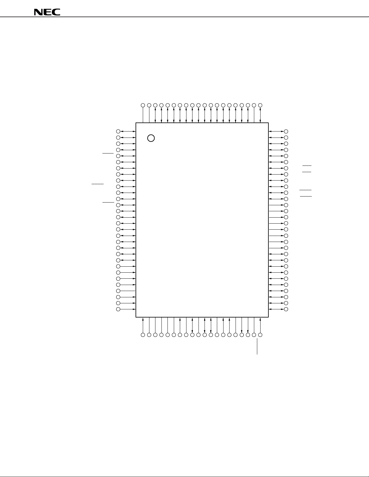
PIN CONFIGURATION (Top View)
• 100-pin plastic QFP (14 × 20)
µ
PD178F098GF-3BA
GNDPORT
PORT
DD
P47
V
P46
P45
P44
P43
P42
P41
P40
P67
P66
P65
P64
P63
P62
P61
P60
GND1
P07/INTP7
µ
PD178F098
P00/INTP0
P01/INTP1
P20/SI1
P21/SO1
P22/SCK1
P23/STB
P24/BUSY
P25/SI0/SB0/SDA0
P26/SO0/SB1/SDA1
P27/SCK0/SCL
P70/SI3
P71/SO3
P72/SCK3
P73
P50
P51
P52
P53
P54
P55
P56
P57
P10/ANI0
P11/ANI1
P12/ANI2
P13/ANI3
AV
P14/ANI4
P15/ANI5
P16/ANI6
100 99 98 97 96 95 94 93 92 91 90 89 88 87 86 85 84 83 82 81
1
2
3
4
5
6
7
8
9
10
11
12
13
14
15
16
17
18
19
20
21
22
23
24
25
26
DD
27
28
29
30
31 32 33 34 35 36 37 38 39 40 41 42 43 44 45 46 47 48 49 50
80
79
78
77
76
75
74
73
72
71
70
69
68
67
66
65
64
63
62
61
60
59
58
57
56
55
54
53
52
51
P06/INTP6
P05/INTP5
P04/INTP4
P124
P123
P122
P121/RX0
P120/TX0
P77
P76
P75/TXD0
P74/RXD0
P137
P136
P135
P134
P133
P132
P131/TO51
P130/TO50
P37/BUZ
P36/BEEP0
P35/TI51
P34/TI50
P33/TI01
P32/TI00
P31/TO0
P30/VM45
P03/INTP3
P02/INTP2
SS
AV
REGCPU
P17/ANI7
DD
V
REGOSC
X2
X1
P100
GND0
GND2
P102/FMIFC
P101/AMIFC
PLL
DD
V
VCOL
VCOH
GNDPLL
EO0
EO1
PP
V
RESET
Cautions 1. Directly connect the VPP pin to GND0, GND1, or GND2 in normal operating mode.
2. Keep the voltage at AV
DD, VDDPORT, and VDDPLL same as that at the VDD pin.
3. Keep the voltage at AVSS, GNDPORT, and GNDPLL same as that at GND0, GND1, or GND2.
4. Connect each of the REGOSC and REGCPU pins to GND via a 0.1-µF capacitor.
Data Sheet U12920EJ1V0DS00
5
Page 6

Pin Name
AMIFC : AM intermediate frequency counter
input
ANI0-ANI7 : A/D converter input
DD : A/D converter power supply
AV
SS : A/D converter ground
AV
BUSY : Busy output
BEEP0, BUZ : Buzzer output
EO0, EO1 : Error out output
FMIFC : FM intermediate frequency counter
input
GNDPLL : PLL ground
GND0-GND2 : Ground
INTP0-INTP7 : Interrupt input
P00-P07 : Port 0
P10-P17 : Port 1
P20-P27 : Port 2
P30-P37 : Port 3
P40-P47 : Port 4
P50-P57 : Port 5
P60-P67 : Port 6
P70-P77 : Port 7
P100-P102 : Port 10
P120-P124 : Port 12
P130-P137 : Port 13
REGCPU : Regulator for CPU power supply
µ
PD178F098
REGOSC : Regulator for oscillation circuit
RESET : Reset input
RXD0 : UART0 serial data input
RX0 : IEBus serial data input
SB0, SB1 : Serial data bus input/output
SCK0, SCK1, SCK3
: Serial clock input/output
SCL : Serial clock input/output
SDA0, SDA1 : Serial data input/output
SI0, SI1, SI3 : Serial data input
SO0, SO1, SO3 : Serial data output
STB : Strobe output
TI00, TI01 : 16-bit timer capture trigger input
TI50, TI51 : 8-bit timer clock input
TO0 : 16-bit timer output
TO50, TO51 : 8-bit timer output
TXD0 : UART0 serial data output
TX0 : IEBus serial data output
VCOL, VCOH : Local oscillation input
DDPORT : Port power supply
V
VDDPLL : PLL power supply
DD : Power supply
V
VM45 : VDD = 4.5 V monitor output
VPP : Programming power supply
X1, X2 : Crystal resonator
6
Data Sheet U12920EJ1V0DS00
Page 7
BLOCK DIAGRAM
µ
PD178F098
TO0/P31
TI00/P32
TI01/P33
TI50/P34
TO50/P130
TI51/P35
TO51/P131
SI0/SB0/SDA0/P25
SO0/SB1/SDA1/P26
SCK0/SCL/P27
SI1/P20
SO1/P21
SCK1/P22
STB/P23
BUSY/P24
SI3/P70
SO3/P71
SCK3/P72
RXD0/P74
TXD0/P75
RX0/P121
TX0/P120
INTP0/P00-
INTP7/P07
BEEP0/P36
BUZ/P37
16-bit TIMER/
EVENT COUNTER
8-bit TIMER/
EVENT COUNTER 50
8-bit TIMER/
EVENT COUNTER 51
WATCHDOG TIMER
BASIC TIMER
SERIAL
INTERFACE 0
SERIAL
INTERFACE 1
SERIAL
INTERFACE 3
UART0
IEBus0
INTERRUPT
8
CONTROL
BUZZER OUTPUT
78K/0
CPU
CORE
RAM
(3K bytes)
FLASH
MEMORY
(60K bytes)
PORT 0
PORT 1
PORT 2
PORT 3
PORT 4
PORT 5
PORT 6
PORT 7
PORT10
PORT 12
PORT 13
A/D
CONVERTER
8
8
8
8
8
8
8
8
3
5
8
8
P00-P07
P10-P17
P20-P27
P30-P37
P40-P47
P50-P57
P60-P67
P70-P77
P100-P102
P120-P124
P130-P137
ANI0/P10ANI7/P17
AV
DD
AV
SS
RESET
X1
X2
DD
PORT
V
GNDPORT
V
VM45/P30
REGOSC
REGCPU
GND0
GND1
RESET
SYSTEM
CONTROL
DD
CPU
PERIPHERAL
FREQUENCY
COUNTER
PLL
AMIFC/P101
FMIFC/P102
EO0
EO1
VCOL
VCOH
V
VOLTAGE
REGULATOR
OSC
V
CPU
PLL
VOLTAGE
REGULATOR
DD
PLL
V
GNDPLL
IC
GND2
Data Sheet U12920EJ1V0DS00
7
Page 8

µ
PD178F098
CONTENTS
1. DIFFERENCES BETWEEN µPD178F098 AND MASK ROM MODELS ..................................... 9
2. PIN FUNCTION LIST...................................................................................................................... 10
2.1 Port Pins .................................................................................................................................. 10
2.2 Pins Other Than Port Pins ......................................................................................................11
2.3 I/O Circuits of Pins and Recommended Connections of Unused Pins ............................. 13
3. MEMORY SIZE SELECT REGISTER (IMS)................................................................................. 17
4. INTERNAL EXTENSION RAM SIZE SELECT REGISTER (IXS) .............................................. 18
5. INTERRUPT FUNCTION ................................................................................................................. 19
6. FLASH MEMORY PROGRAMMING .............................................................................................. 23
6.1 Selecting Communication Mode ........................................................................................... 23
6.2 Flash Memory Programming Function ................................................................................. 24
6.3 Connecting Flashpro III .......................................................................................................... 25
7. ELECTRICAL SPECIFICATIONS ................................................................................................... 26
8. PACKAGE DRAWING ..................................................................................................................... 44
9. RECOMMENDED SOLDERING CONDITIONS ............................................................................. 45
APPENDIX A. DEVELOPMENT TOOLS ............................................................................................... 46
APPENDIX B. RELATED DOCUMENTS .............................................................................................. 48
8
Data Sheet U12920EJ1V0DS00
Page 9
µ
PD178F098
1. DIFFERENCES BETWEEN µPD178F098 AND MASK ROM MODELS
The µPD178F098 is provided with a flash memory to/from which data can be written/erased with the device
mounted on a printed circuit board. The differences between the flash memory model (µPD178F098) and mask ROM
µ
models (
PD178076, 178078, 178096, and 178098) are shown in Table 1-1.
µ
Table 1-1. Differences between
PD178F098 and Mask ROM Models
Item
Internal memory ROM structure Flash memory Mask ROM
ROM capacity 60K bytes
External 2048 bytes
extension RAM
Internal ROM capacity selected by Equivalent to mask ROMµPD178076: CCH
memory size select register (IMS) model
Internal extension RAM capacity Equivalent to mask ROMµPD178076: 0AH
selected by internal extension RAM model
size select register (IXS)
Serial interface 4 channels 3 channels
IEBus controller Provided Not provided Provided
Interrupt source 24 22 21
IC pin Not provided Provided
VPP pin Provided Not provided
Electrical specifications and See the relevant data sheet
recommended soldering conditions
µ
PD178F098
• 3-wire/SBI/2-wire/I2C bus mode selectable • 3-wire/SBI/2-wire/I2C bus
• 3-wire (with automatic transmit/receive function) mode selectable
• 3-wire • 3-wire (with automatic
• UART transmit/receive function)
µ
PD178076, 178078
µ
PD178076: 48K bytes
µ
PD178078: 60K bytes
µ
PD178076: 1024 bytes
µ
PD178078: 2048 bytes
µ
PD178078: CFH
µ
PD178078: 08H
µ
PD178096, 178098
µ
PD178096: 48K bytes
µ
PD178098: 60K bytes
µ
PD178096: 1024 bytes
µ
PD178098: 2048 bytes
µ
PD178096: CCH
µ
PD178098: CFH
µ
PD178096: 0AH
µ
PD178098: 08H
• 3-wire
Caution The noise resistance and noise radiation differ between flash memory versions and mask ROM
versions. When considering the replacement of flash memory versions with mask ROM versions
in the process from trial manufacturing to mass production, adequate evaluation should be carried
out using CS products (not ES products) of mask ROM versions.
Data Sheet U12920EJ1V0DS00
9
Page 10
µ
PD178F098
2. PIN FUNCTION LIST
2.1 Port Pins (1/2)
Pin Name I/O Function At Reset Shared by:
P00-P07 I/O Port 0. Input INTP0-INTP7
8-bit I/O port.
Can be set in input or output mode in 1-bit units.
P10-P17 Input Port 1. Input ANI0-ANI7
8-bit input port.
P20 I/O Port 2. Input SI1
P21 8-bit I/O port. SO1
P22 Can be set in input or output mode in 1-bit units. SCK1
P23 STB
P24 BUSY
P25 SI0/SB0/SDA0
P26 SO0/SB1/SDA1
P27 SCK0/SCL
P30 I/O Port 3. Input VM45
P31 8-bit I/O port. TO0
P32 Can be set in input or output mode in 1-bit units. TI00
P33 TI01
P34 TI50
P35 TI51
P36 BEEP0
P37 BUZ
P40-47 I/O Port 4. Input –
8-bit I/O port.
Can be set in input or output mode in 1-bit units.
P50-P57 I/O Port 5. Input –
8-bit I/O port.
Can be set in input or output mode in 1-bit units.
P60-P67 I/O Port 6. Input –
8-bit I/O port.
Can be set in input or output mode in 1-bit units.
P70 I/O Port 7. Input SI3
P71 8-bit I/O port. SO3
P72 Can be set in input or output mode in 1-bit units. SCK3
P73 –
P74 RXD0
P75 TXD0
P76, P77 –
10
Data Sheet U12920EJ1V0DS00
Page 11
µ
PD178F098
2.1 Port Pins (2/2)
Pin Name I/O Function At Reset Shared by:
P100 I/O Port 10. Input –
P101 3-bit I/O port. AMIFC
P102 Can be set in input or output mode in 1-bit units. FMIFC
P120 I/O Port 12. Input TX0
P121 5-bit I/O port. RX0
P122-P124 Can be set in input or output mode in 1-bit units. –
P130 Output Port 13. Low-level TO50
P131 8-bit output port. output TO51
P132-P137 N-ch open-drain output port (15 V withstand) –
2.2 Pins Other Than Port Pins (1/2)
Pin Name I/O Function At Reset Shared by:
INTP0-INTP7 Input External maskable interrupt input whose valid edge Input P00-P07
(rising edge, falling edge, or both rising and falling edges)
can be specified.
SI0 Input Serial data input to serial interface. Input P25/SB0/SDA0
SI1 P20
SI3 P70
SO0 Output Serial data output from serial interface. Input P26/SB1/SDA1
SO1 P21
SO3 P71
SB0 I/O Serial data input/output to/from N-ch open drain I/O Input P25/SI0/SDA0
SB1 serial interface. P26/SO0/SDA1
SDA0 P25/SI0/SB0
SDA1 P26/SO0/SB1
SCK0 I/O Serial clock input/output to/from serial interface. Input P27/SCL
SCK1 P22
SCK3 P72
SCL N-ch open drain I/O P27/SCK0
STB Output Strobe output for serial interface automatic transmission/ Input P23
reception.
BUSY Input Busy input for serial interface automatic transmission/ Input P24
reception.
VW45 Output VDD = 4.5 V monitor output Input P30
TI00 Input External count clock input to 16-bit timer (TM0). Input P32
TI01 P33
TI50 Input External count clock input to 8-bit timer (TM50). Input P34
TI51 External count clock input to 8-bit timer (TM51). P35
TO0 Output 16-bit timer (TM0) output. Input P31
TO50 8-bit timer (TM50) output. Low-level P130
TO51 8-bit timer (TM51) output. output P131
BEEP0 Output Buzzer output. Input P36
BUZ P37
Data Sheet U12920EJ1V0DS00
11
Page 12
µ
PD178F098
2.2 Pins Other Than Port Pins (2/2)
Pin Name I/O Function At Reset Shared by:
ANI0-ANI7 Input Analog input to A/D converter. Input P10-P17
EO0, EO1 Output Error out output from charge pump of PLL frequency – –
synthesizer.
VCOL Input Inputs local oscillation frequency of PLL (in HF and MF – –
modes).
VCOH Input Inputs local oscillation frequency of PLL (in VHF mode). – –
AMIFC Input Input to AM intermediate frequency counter. Input P101
FMIFC Input Input to FM intermediate frequency or AM intermediate Input P102
frequency counter.
RXD0 Input Serial data input to asynchronous serial interface (UART0). Input P74
TXD0 Output Serial data output from asynchronous serial interface Input P75
(UART0).
TX0 Output IEBus controller data output. Input P120
RX0 Input IEBus controller data input. Input P121
RESET Input System reset input. – –
X1 Input Connection of crystal resonator for system clock oscillation. – –
X2 – ––
REGOSC – Regulator for oscillation circuit. Connect this pin to GND via – –
0.1-µF capacitor.
REGCPU – Regulator for CPU power supply. Connect this pin to GND – –
via 0.1-µF capacitor.
VDD – Positive power supply. – –
GND0-GND2 – Ground. – –
VDDPORT – Port power supply. – –
GNDPORT – Port ground. – –
AVDD – A/D converter positive power supply. Keep voltage at this – –
pin same as that at VDD0.
AVSS – A/D converter ground. Keep voltage at this pin same as – –
that at GND0 through GND2.
Note
VDDPLL
GNDPLL
VPP – Pin to apply high voltage at program writing/verifying. – –
Note
– PLL positive power supply. – –
– PLL ground. – –
Directly connect this pin to GND0, GND1, or GND2 in
normal operating mode.
Note Connect a capacitor of about 1000 pF between the VDDPLL and GNDPLL pins.
12
Data Sheet U12920EJ1V0DS00
Page 13
µ
PD178F098
2.3 I/O Circuits of Pins and Recommended Connections of Unused Pins
Table 2-1 shows the types of the I/O circuits of the respective pins and the recommended connections of the pins
when they are not used.
For the configuration of the I/O circuit of each pin, refer to Figure 2-1.
Table 2-1. I/O Circuit Type of Each Pin (1/2)
Pin Name I/O Circuit Type I/O Recommended Connection of Unused Pin
P00/INTP0-P07/INTP7 8 I/O Input: Connect each of them to VDD, VDDPORT, GND0 to
GND2, or GNDPORT via resistor.
Output: Leave open.
P10/ANI0-P17/ANI7 25 Input Connect these pins to VDD, VDDPORT, GND0 to GND2 or
GNDPORT.
P20/SI1 5-K I/O Input: Connect each of them to VDD, VDDPORT, GND0 to
P21/SO1 5
P22/SCK1 5-K
P23/STB 5
P24/BUSY 5-K
P25/SI0/SB0/SDA0 10-D
P26/SO0/SB1/SDA1
P27/SCK0/SCL
P30/VM45 5
P31/TO0
P32/TI00 5-K
P33/TI01
P34/TI50
P35/TI51
P36/BEEP0 5
P37/BUZ
P40-P47
P50-P57
P60-P67
P70/SI3 5-K
P71/SO3 5
P72/SCK3 5-K
P73 5
P74/RXD0 5-K
P75/TXD0 5
P76, P77
P100
P101/AMIFC
P102/FMIFC
P120/TX0
P121/RX0 5-K
P122-P124 5
GND2, or GNDPORT via resistor.
Output: Leave open.
Data Sheet U12920EJ1V0DS00
13
Page 14
µ
PD178F098
Table 2-1. I/O Circuit Type of Each Pin (2/2)
Pin Name I/O Circuit Type I/O Recommended Connection of Unused Pin
P130/TO50 19 Output Open these pins.
P131/TO51
P132-P137
EO0 DTS-EO1
EO1
VCOL, VCOH DTS-AMP2 Input Disable PLL in software and select pull-down.
REGOSC, REGCPU – – Connect these pins to GND0, GND1, or GND2 via 0.1-µF
capacitor.
RESET 2 Input –
AVDD – – Connect this pin to VDD or VDDPORT.
AVSS Directly connect these pins to GND0 to GND2, or GNDPORT.
VPP
14
Data Sheet U12920EJ1V0DS00
Page 15
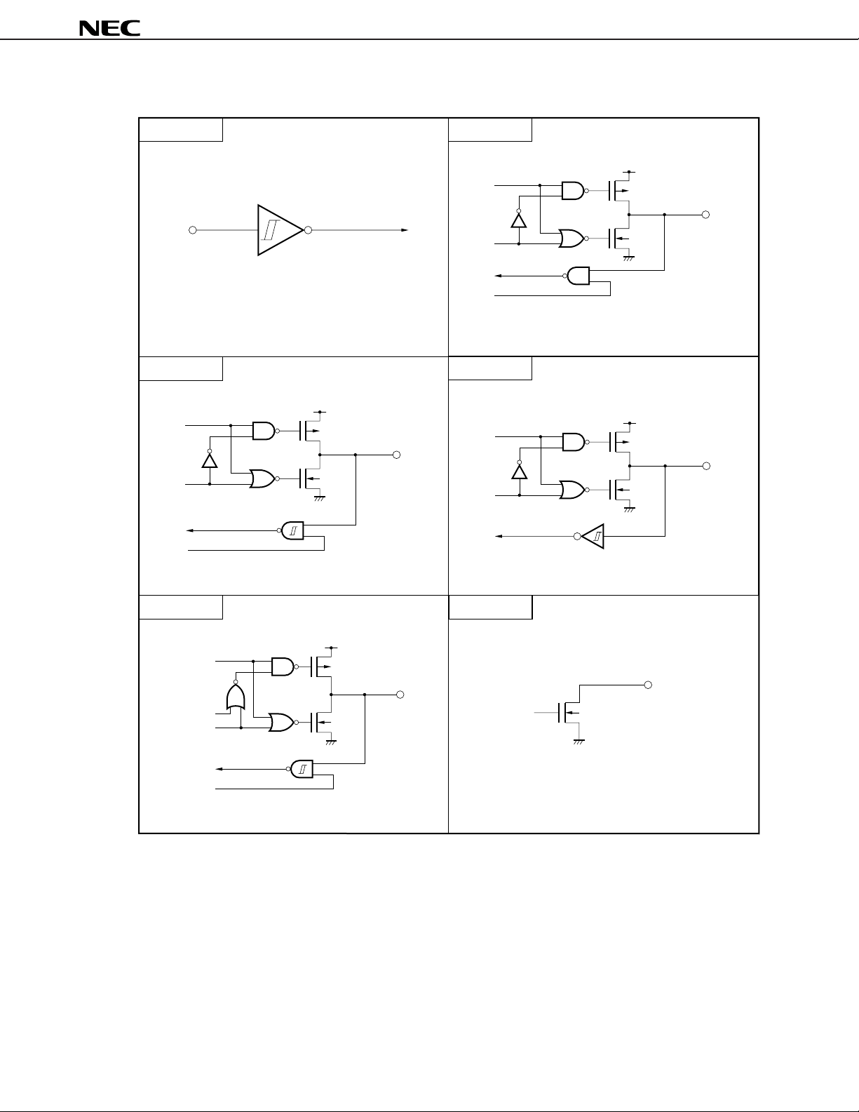
Figure 2-1. I/O Circuits of Respective Pins (1/2)
µ
PD178F098
Type 2
IN
Schmitt trigger input with hysteresis characteristics
Type 5-K
V
DD
data
output
disable
P-ch
N-ch
IN/OUT
Type 5
data
output
disable
input
enable
Type 8
data
output
disable
V
V
DD
P-ch
IN/OUT
N-ch
DD
P-ch
IN/OUT
N-ch
input
enable
Type 10-D
data
open drain
output disable
input
enable
Remark V
Type 19
V
DD
P-ch
IN/OUT
N-ch
DD and GND are the positive power supply and ground pins for all port pins. Take VDD and GND as
N-ch
OUT
VDDPORT and GNDPORT.
Data Sheet U12920EJ1V0DS00
15
Page 16
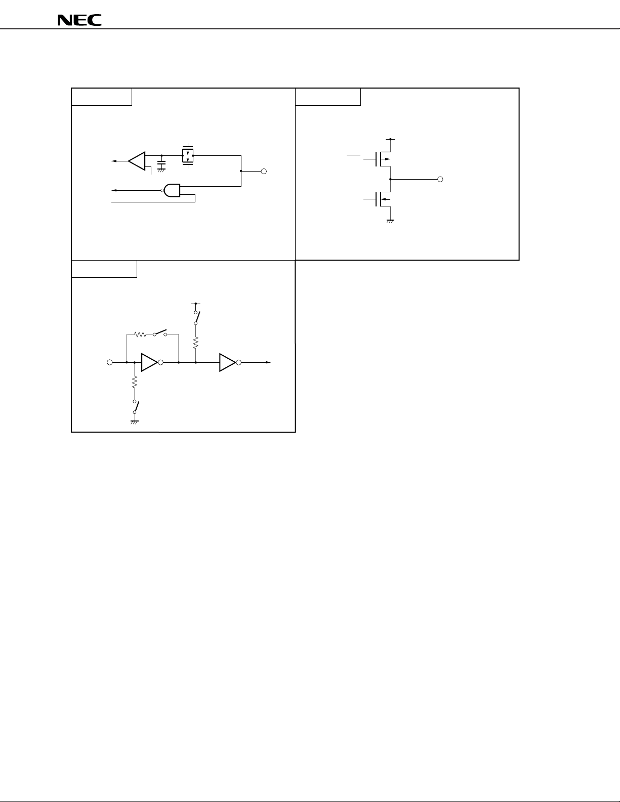
Figure 2-1. I/O Circuits of Respective Pins (2/2)
µ
PD178F098
Type 25
Comparator
input
enable
Type DTS-AMP
IN
P-ch
+
–
N-ch
V
REF (Threshold voltage)
VDDPLL
IN
Type DTS-EO1
DW
UP
DDPLL
V
P-ch
OUT
N-ch
GNDPLL
Note
GNDPLL
Note This switch is selectable in software only for the VCOL and VCOH pins.
Remark VDD and GND are the positive power supply and ground pins for all port pins. Take VDD and GND as
VDDPORT and GNDPORT.
16
Data Sheet U12920EJ1V0DS00
Page 17

µ
PD178F098
3. MEMORY SIZE SELECT REGISTER (IMS)
The internal memory capacity of the µPD178F098 can be changed using the memory size select register (IMS).
µ
By using this register, the memory of the
with a different internal memory capacity.
Use an 8-bit memory manipulation instruction to set the IMS.
This register is set to CFH at reset.
Figure 3-1. Format of Memory Size Select Register (IMS)
PD178F098 can be mapped in the same manner as a mask ROM model
Symbol
RAM2 RAM1 RAM0 Selects internal high-speed RAM capacity
Others Setting prohibited
RAM3 RAM2 RAM1 RAM0 Selects internal ROM capacity
Others Setting prohibited
7
RAM26RAM15RAM0403ROM32ROM21ROM10ROM0
IMS
1 1 0 1024 bytes
1 1 0 0 48K bytes
1 1 1 1 60K bytes
Address
FFF0H
At reset
CFH
R/W
R/W
Table 3-1 shows the setting of IMS to perform the same memory mapping as that of a mask ROM model.
Table 3-1. Setting of Memory Size Select Register
Targeted Model Setting of IMS
µ
PD178076, 178096 CCH
µ
PD178078, 178098 CFH
Data Sheet U12920EJ1V0DS00
17
Page 18

µ
PD178F098
4. INTERNAL EXTENSION RAM SIZE SELECT REGISTER (IXS)
The internal extention RAM capacity of the µPD178F098 can be changed using the internal extention RAM size
select register (IXS). By using this register, the memory of the µPD178F098 can be mapped in the same manner
as a mask ROM model with a different internal extention RAM capacity.
Use an 8-bit memory manipulation instruction to set the IXS.
This register is set to 0CH at reset.
Figure 4-1. Format of Internal Extension RAM Size Select Register (IXS)
7
6
5
4
3
2
1
Symbol
IXS
0
0
0
IXRAM4
I
XRAM3
I
XRAM2
I
XRAM1
0
I
XRAM0
Address
FFF4H
At reset
0CH
R/W
R/W
IXRAM4 IXRAM3 IXRAM2 IXRAM1 IXRAM0
0 1 0 0 0 2048 bytes
0 1 0 1 0 1024 bytes
Others Setting prohibited
Selects internal extension RAM capacity
Table 4-1 shows the setting of IXS to perform the same memory mapping as that of a mask ROM model.
Table 4-1. Setting of Internal RAM Size Select Register
Targeted Model Setting of IXS
µ
PD178076, 178096 0AH
µ
PD178078, 178098 08H
18
Data Sheet U12920EJ1V0DS00
Page 19

µ
PD178F098
5. INTERRUPT FUNCTION
The µPD178F098 has the following three types and 24 sources of interrupts:
• Non-maskable : 1
• Maskable : 23
• Software : 1
Note Two types of watchdog interrupt sources (INTWDT), non-maskable and maskable, are available, and
either of them can be selected.
Note
Note
Table 5-1. Interrupt Sources (1/2)
Interrupt Type
Non-maskable – INTWDT Overflow of watchdog timer Internal 0004H (A)
Maskable 0 INTWDT Overflow of watchdog timer (B)
Default
Note 1
Priority
1 INTP0 Pin input edge detection External 0006H (C)
2 INTP1 0008H
3 INTP2 000AH
4 INTP3 000CH
5 INTP4 000EH
6 INTP5 0010H
7 INTP6 0012H
8 INTP7 0014H
9 INTCSI0 End of transfer by serial interface 0 Internal 0016H (B)
10 INTCSI1 End of transfer by serial interface 1 0018H
11 INTCSI3 End of transfer by serial interface 3 001AH
12 INTTM50 Generation of coincidence signal of 8-bit 001CH
13 INTTM51 Generation of coincidence signal of 8-bit 001EH
14 INTSER0 Reception error of serial interface UART0 0020H
15 INTSR0 End of reception by serial interface UART0 0022H
16 INTST0
17 INTBTM0 Generation of coincidence signal of basic 0026H
Name Trigger
(when watchdog timer mode 1 is selected)
(when interval timer mode is selected)
timer/event counter 50
timer/event counter 51
End of transmission by serial interface UART0
timer
Interrupt Source
Internal/
External
Vector Basic
Table Configuration
Address Type
0024H
Note 2
Notes 1. If two or more maskable interrupts occur at the same time, they are acknowledged or kept pending
according to their default priorities. The default priority 0 is the highest, while 22 is the lowest.
2. (A) to (E) under the heading Basic Configuration Type corresponds to (A) to (E) in Figure 5-1.
Data Sheet U12920EJ1V0DS00
19
Page 20

Table 5-1. Interrupt Sources (2/2)
µ
PD178F098
Interrupt Type
Maskable 18 INTTM00 Generation of signal indicating coincidence Internal 0028H (B)
Software – BRK Execution of BRK instruction – 003EH (E)
Default
Note 1
Priority
19 INTTM01 Generation of signal indicating coincidence Internal 002AH (B)
20 INTIE1 IEBus0 data access request Internal 002CH (B)
21 INTIE2 IEBus0 communication error and start/end 002EH
22 INTAD End of conversion by A/D converter AD1 0030H (B)
Name Trigger
between 16-bit timer counter (TM0) and
capture/compare register (CR00) (when
CR00 is used as compare register)
Detection of input edge of TI00/P32 pin External (D)
(when CR00 is used as capture register)
between 16-bit timer counter (TM0) and
capture/compare register (CR01) (when
CR01 is used as compare register)
Detection of input edge of TI01/P33 pin External (D)
(when CR01 is used as capture register)
of communication
Interrupt Source
Internal/
External
Vector Basic
Table Configuration
Address Type
Note 2
Notes 1. If two or more maskable interrupts occur at the same time, they are acknowledged or kept pending
according to their default priorities. The default priority 0 is the highest, while 22 is the lowest.
2. (A) to (E) under the heading Basic Configuration Type corresponds to (A) to (E) in Figure 5-1.
20
Data Sheet U12920EJ1V0DS00
Page 21

Figure 5-1. Basic Configuration of Interrupt Function (1/2)
g
g
(A) Internal non-maskable interrupt
Internal bus
µ
PD178F098
Interrupt
request
(B) Internal maskable interrupt
Interrupt
request
IF
Priority control
circuit
Internal bus
MK IE PR ISP
Priority control
circuit
Vector table
address generation
circuit
Standby release
signal
Vector table
address generation
circuit
Standby release
si
nal
(C) External maskable interrupt (INTP0 through INTP7)
Internal bus
External interrupt
Interrupt
request
rising/falling edge enable
registers (EGP, EGN)
Edge detection
circuit
MK IE PR ISP
IF
Data Sheet U12920EJ1V0DS00
Priority control
circuit
Vector table
address generation
circuit
Standby release
si
nal
21
Page 22

Figure 5-1. Basic Configuration of Interrupt Function (2/2)
(D) External maskable interrupts (INTTM00, INTTM01)
Internal bus
µ
PD178F098
Prescaler mode register
Interrupt
request
(E) Software interrupt
Interrupt
request
(PRM0)
Edge detection
circuit
MK
IF
Priority control
circuit
PR
Priority control
circuit
Internal bus
ISPIE
Vector table
address generation
circuit
Standby release
signal
Vector table
address generation
circuit
Remark IF : Interrupt request flag
IE : Interrupt enable flag
ISP: In-service priority flag
MK : Interrupt mask flag
PR : Priority specification flag
22
Data Sheet U12920EJ1V0DS00
Page 23

µ
PD178F098
6. FLASH MEMORY PROGRAMMING
The program memory provided in the µPD178F098 is flash memory.
The flash memory can be written on-board, i.e., with the µPD178F098 mounted on the target system.
To do so, connect a dedicated flash writer (Flashpro III (Part number FL-PR3, PG-FP3)) to the host machine and
target system.
Remark FL-PR3 is a product of Naito Densei Machida Mfg. Co., Ltd.
6.1 Selecting Communication Mode
The flash memory is written by using Flashpro III and by means of serial communication. Select a communication
mode from those listed in Table 6-1. To select a communication mode, the format shown in Figure 6-1 is used. Each
communication mode is selected depending on the number of V
Table 6-1. Communication Modes
Communication Mode Number of Channels Pins Used Number of VPP Pulses
3-wire serial I/O (SIO3) 1 SI3/P70 0
SO3/P71
SCK3/P72
UART0 1 RXD0/P74 8
TXD0/P75
PP pulses shown in Table 6-1.
Caution Be sure to select a communication mode by the number of VPP pulses shown in Table 6-1.
Figure 6-1. Communication Mode Selection Format
V
PP pulse
10 V
VPP
RESET
DD
V
GND
DD
V
GND Flash memory writing mode
Data Sheet U12920EJ1V0DS00
23
Page 24

µ
PD178F098
6.2 Flash Memory Programming Function
An operation such as writing the flash memory is performed when a command or data is transmitted/received in
the selected communication mode. The major flash memory programming functions are listed in Table 6-2.
Table 6-2. Major Flash Memory Programming Functions
Function Description
Batch erase Erases all memory contents.
Batch blank check Checks erased status of entire memory.
Data write Writes data to flash memory starting from write start address and based on number
of data (bytes) to be written).
Batch verify Compares all contents of memory with input data.
24
Data Sheet U12920EJ1V0DS00
Page 25

µ
Flashpro III PD178F098
µ
V
PP
V
DD
RESET
CLK
SO
SI
GND
V
PP
V
DD
RESET
X1
RXD0
TXD0
GND
PD178F098
6.3 Connecting Flashpro III
Connection with Flashpro III differs depending on the communication mode (3-wire serial I/O or UART0). Figures
6-2 and 6-3 show the connection in the respective modes.
Figure 6-2. Connection of Flashpro III in 3-Wire Serial I/O Mode
Flashpro III PD178F098
V
PP
V
DD
RESET
CLK
SCK
SO
SI
GND
µ
V
PP
V
DD
RESET
X1
SCK3
SI3
SO3
GND
Figure 6-3. Connection of Flashpro III in UART0 Mode
Data Sheet U12920EJ1V0DS00
25
Page 26

µ
PD178F098
7. ELECTRICAL SPECIFICATIONS
Absolute Maximum Ratings (TA = 25°C)
Parameter Symbol Conditions Rating Unit
Supply voltage VDD –0.3 to +6.0 V
VDDPORT
AVDD –0.3 to VDD + 0.3
VDDPLL –0.3 to VDD + 0.3
VPP –0.3 to +10.5 V
Input voltage VI –0.3 to VDD + 0.3 V
Output voltage VO Excluding P130 to P137 –0.3 to VDD + 0.3 V
Output breakdown VBDS P130-P137 N-ch open drain 16 V
voltage
Analog input voltage
High-level output IOH 1 pin –8 mA
current Total of P00-P01, P20-P27, P50-P57, and P70-P73 –15 m A
Low-level output IOL
current r.m.s 8 mA
Operating temperature
Storage temperature Tstg –55 to +125 °C
VAN P10-P17 Analog input pin –0.3 to VDD + 0.3 V
Total of P02-P07, P30-P37, P40-P47, P60-P67, –15 mA
P74-P77, and P120-P124
Total of P100-P102 –10 mA
Note 2
1 pin Peak value 16 mA
Total of P00-P01, P20-P27, P50-P57, Peak value 30 mA
and P70-P73 r.m.s 15 mA
Total of P02-P07, P30-P37, P40-P47, Peak value 30 mA
P60-P67, P74-P77, P120-P124, and r.m.s 15 mA
P130-P137
Total of P100-102 Peak value 20 mA
r.m.s 10 mA
TA During normal operation –40 to +85 °C
During flash memory programming 10 to 40 °C
–0.3 to VDD + 0.3
Note 1
Note 1
Note 1
V
V
V
Notes 1. Keep the voltage at VDDPORT, AVDD, and VDDPLL same as that at the VDD pin.
2. Calculate the r.m.s as follows: [r.m.s] = [Peak value] x √Duty
Caution If the rated value of even one of the above parameters is exceeded even momentarily, the quality
of the product may be degraded. The absolute maximum ratings, therefore, are the values
exceeding which the product may be physically damaged. Be sure to use the product with these
ratings never being exceeded.
Remark Unless otherwise specified, the characteristics of a multiplexed pin are the same as those of the
corresponding port pin.
26
Data Sheet U12920EJ1V0DS00
Page 27

µ
PD178F098
Recommended Supply Voltage Ranges (TA = –40 to +85°C)
Parameter Symbol Conditions MIN. TYP. MAX. Unit
Supply voltage VDD1 When CPU and PLL are operating 4.5 5.0 5.5 V
VDD2 When CPU is operating and PLL is stopped 3.5 5.0 5.5 V
Data retention voltage
Output breakdown VBDS P130-P137 (N-ch open drain) 15 V
voltage
VDDR When crystal oscillation stops 2.3 5.5 V
DC Characteristics (TA = –40 to +85°C, VDD = 3.5 to 5.5 V)
Parameter Symbol Test Conditions MIN. TYP. MAX. Unit
High-level input VIH1 P10-P17, P21, P23, P30, P31, P36, P37, P40-P47, 0.7 VDD VDD V
voltage P50-P57, P60-P67, P71, P73, P75-P77, P100-P102,
P120, P122-P124
VIH2 P00-P07, P20, P22, P24-P27, P32-P35, P70, P72, 0.8 VDD V DD V
P74, P121, RESET
Low-level input VIL1 P10-P17, P21, P23, P30, P31, P36, P37, P40-P47, 0 0.3 VDD V
voltage P50-P57, P60-P67, P71, P73, P75-P77, P100-P102,
P120, P122-P124
VIL2 P00-P07, P20, P22, P24-P27, P32-P35, P70, P72, 0 0.2 VDD V
P74, P121, RESET
High-level output VOH1
voltage
VOH2 EO0, EO1 VDD = 4.5 to 5.5 V, VDD – 1.0 V
Low-level output VOH1
voltage
High-level input ILIH P00-P07, P10-P17, VI = VDD 3
leakage current P20-P24, P30-P37,
P00-P07, P20-P24, P30-P37,
P40-P47, P50-P57, P60-P67,
P70-P77, P100-P102,
P120-P124
P00-P07, P20-P27, P30-P37,
P40-P47, P50-P57, P60-P67,
P70-P77, P100-P102,
P120-P124, P130-P137,
VOL2 EO0, EO1 VDD = 4.5 to 5.5 V, 1.0 V
P40-P47, P50-P57,
P60-P67, P70-P77,
P100-P102, P120-P124,
RESET
4.5 V ≤ VDD ≤ 5.5 V, VDD – 1.0 V
IOH = –1 mA
3.5 V ≤ VDD < 4.5 V, VDD – 0.5 V
IOH = –100 µA
IOH = –3 mA
4.5 V ≤ VDD ≤ 5.5 V, 1.0 V
IOL = 1 mA
3.5 V ≤ VDD < 4.5 V, 0.5 V
IOL = 100 µA
IOL = 3 mA
µ
A
Remark Unless otherwise specified, the characteristics of a multiplexed pin are the same as those of the
corresponding port pin.
Data Sheet U12920EJ1V0DS00
27
Page 28

DC Characteristics (TA = –40 to +85°C, VDD = 3.5 to 5.5 V)
Parameter Symbol Conditions MIN. TYP. MAX. Unit
Low-level input ILIL P00-P07, P10-P17, VI = 0 V –3
leakage current P20-P27, P30-P37,
P40-P47, P50-P57,
P60-P67, P70-P77,
P100-P102, P120-P124,
RESET
Output off
leakage current
Supply current
Note
ILOH1 P130-P137 VO = 15 V –3
ILOL1 P130-P137 VO = 0 V 3
ILOH2 P25-P27 VO = VDD –3
(at N-ch open drain I/O)
ILOL2 P25-P27 VO = 0 V 3
(at N-ch open drain I/O)
ILOH3 EO0, EO1 VO = VDD –3
ILOL3 EO0, EO1 VO = 0 V 3
IDD1 fx = 4.5 MHz 5.0 18 mA
IDD2 fx = 6.3 MHz 7.0 20 mA
When CPU is operating
and PLL is stopped.
Sine wave input to X1 pin
VI = VDD
µ
PD178F098
µ
A
µ
A
µ
A
µ
A
µ
A
µ
A
µ
A
IDD3 fx = 4.5 MHz 0.3 0.8 mA
IDD4 fx = 6.3 MHz 0.4 1.0 mA
Data retention
voltage
Data retention IDDR1 When crystal oscillation is TA = 25°C, 2.0 4.0
current stopped VDD = 5 V
VDDR1 When crystal resonator is oscillating 3.5 5.5 V
VDDR2 When crystal oscillation is Power-failure detection 2.2 V
VDDR3 Data memory retained 2.0 V
IDDR2 2.0 20
In HALT mode with PLL
stopped.
Sine wave input to X1 pin
VI = VDD
stopped function
Note Excluding AVDD current and VDDPLL current.
Remarks 1. f
X: System clock oscillation frequency
2. Unless otherwise specified, the characteristics of a multiplexed pin are the same as those of the
corresponding port pin.
µ
A
µ
A
28
Data Sheet U12920EJ1V0DS00
Page 29

µ
PD178F098
Reference Characteristics (TA = –40 to +85°C, VDD = 4.5 to 5.5 V)
Parameter Symbol Conditions MIN. TYP. MAX. Unit
Supply current IDD5 When CPU and PLL are operating. 8 mA
Sine wave input to VCOH pin
At fIN = 160 MHz, VIN = 0.15 VP-P
AC Characteristics
(1) Basic operation (TA = –40 to +85°C, VDD = 3.5 to 5.5 V)
Parameter Symbol Conditions MIN. TYP. MAX. Unit
Cycle time
(minimum instruction
execution time)
TI00, TI01 input tTIH0,
high-/low-level tTIL0
widths
TI50, TI51 input fTI5 2 MHz
frequency
TI50, TI51 input tTIH5, 200 ns
high-/low-level tTIL5
widths
Interrupt input tINTH, INTP0-INTP7 1
high-/low-level tINTL
widths
RESET pin tRSL 10
low-level width
TCY At fX = 6.3 MHz 0.32 5.08
At fX = 4.5 MHz
Note 1
0.44 7.11
Note 2
4/fsam
µ
s
µ
s
s
µ
s
µ
s
Notes 1. Only when products not using IEBus are supported.
2. fsam = fX/2, fX/4, fX/64 selectable by bits 0 and 1 (PRM00 and PRM01) of the prescaler mode register
0 (PRM0). However, fsam = fX/8 when the valid edge of TI00 is selected as the count clock.
Data Sheet U12920EJ1V0DS00
29
Page 30

µ
PD178F098
(2) Serial interface (TA = –40 to +85°C, VDD = 3.5 to 5.5 V)
(a) Serial interface 0
(i) 3-wire serial I/O mode (SCK0 ... internal clock output)
Parameter Symbol Test Conditions MIN. TYP. MAX. Unit
SCK0 cycle time tKCY1 VDD = 4.5 to 5.5 V 800 ns
1600 ns
SCK0 high-/low-level width tKH1,VDD = 4.5 to 5.5 V
tKL1
SI0 setup time (to SCK0↑)tSIK1 VDD = 4.5 to 5.5 V 100 ns
SI0 hold time (from SCK0↑)tKSI1 400 ns
SO0 output delay time from SCK0↓
tKSO1 C = 100 pF
Note
tKCY1/2 – 50
tKCY1/2 – 100
150 ns
300 ns
ns
ns
Note C is the load capacitance of SCK0 and SO0 output line.
(ii) 3-wire serial I/O mode (SCK0 ... external clock input)
Parameter Symbol Test Conditions MIN. TYP. MAX. Unit
SCK0 cycle time tKCY2 VDD = 4.5 to 5.5 V 800 ns
1600 ns
SCK0 high-/low-level width tKH2,VDD = 4.5 to 5.5 V 400 ns
tKL2
SI0 setup time (to SCK0↑)tSIK2 100 ns
SI0 hold time (from SCK0↑)tKSI2 400 ns
SO0 output delay time from SCK0↓
tKSO2 C = 100 pF
Note
800 ns
300 ns
SCK0 at rising or falling edge time tR2, tF2 1000 ns
Note C is the load capacitance of SO0 output line.
30
Data Sheet U12920EJ1V0DS00
Page 31

µ
PD178F098
(iii) SBI mode (SCK0 ... internal clock output)
Parameter Symbol Test Conditions MIN. TYP. MAX. Unit
SCK0 cycle time tKCY3 VDD = 4.5 to 5.5 V 800 ns
3200 ns
SCK0 high-/low-level width tKH3,VDD = 4.5 to 5.5 V
tKL3
SB0, SB1 setup time (to SCK0↑)tSIK3 VDD = 4.5 to 5.5 V 100 ns
SB0, SB1 hold time (from SCK0↑)
SB0, SB1 output delay time from tKSO3 R = 1 kΩ VDD = 4.5 to 5.5 V 0 250 ns
SCK0↓
SB0, SB1↓ from SCK0
SCK0↓ from SB0, SB1↓ tSBK tKCY3 ns
SB0, SB1 high-level width tSBH tKCY3 ns
SB0, SB1 low-level width tSBL tKCY3 ns
↑
tKSI3 tKCY3/2 ns
C = 100 pF
tKSB tKCY3 ns
Note
tKCY3/2 – 50
tKCY3/2 – 150
300 ns
0 1000 ns
Note R and C are the load resistance and load capacitance of SCK0, SB0 and SB1 output line.
(iv) SBI mode (SCK0 ... external clock input)
Parameter Symbol Test Conditions MIN. TYP. MAX. Unit
SCK0 cycle time tKCY4 VDD = 4.5 to 5.5 V 800 ns
3200 ns
ns
ns
SCK0 high-/low-level width tKH4,VDD = 4.5 to 5.5 V 400 ns
tKL4
SB0, SB1 setup time (to SCK0↑)tSIK4 VDD = 4.5 to 5.5 V 100 ns
SB0, SB1 hold time (from SCK0↑)
SB0, SB1 output delay time from tKSO4 R = 1 kΩ VDD = 4.5 to 5.5 V 0 250 ns
SCK0↓
SB0, SB1↓ from SCK0
SCK0↓ from SB0, SB1↓ tSBK tKCY4 ns
SB0, SB1 high-level width tSBH tKCY4 ns
SB0, SB1 low-level width tSBL tKCY4 ns
SCK0 at rising or falling edge time tR4, tF4 1000 ns
↑
tKSI4 tKCY4/2 ns
C = 100 pF
tKSB tKCY4 ns
Note
1600 ns
300 ns
0 1000 ns
Note R and C are the load resistance and load capacitance of SB0 and SB1 output line.
Data Sheet U12920EJ1V0DS00
31
Page 32

µ
PD178F098
(v) 2-wire serial I/O mode (SCK0 ... internal clock output)
Parameter Symbol Test Conditions MIN. TYP. MAX. Unit
SCK0 cycle time tKCY5 R = 1 kΩ 1600 ns
SCK0 high-level width tKH5
C = 100 pF
Note
tKCY5/2 – 160
ns
SCK0 low-level width tKL5 VDD = 4.5 to 5.5 V
SB0, SB1 setup time (to SCK0↑)tSIK5 VDD = 4.5 to 5.5 V 300 ns
SB0, SB1 hold time (from SCK0↑)
SB0, SB1 output delay time from tKSO5 0 300 ns
SCK0↓
tKSI5 600 ns
tKCY5/2 – 50
tKCY5/2 – 100
350 ns
ns
ns
Note R and C are the load resistance and load capacitance of SCK0, SB0 and SB1 output line.
(vi) 2-wire serial I/O mode (SCK0 ... external clock input)
Parameter Symbol Test Conditions MIN. TYP. MAX. Unit
SCK0 cycle time tKCY6 1600 ns
SCK0 high-level width tKH6 650 ns
SCK0 low-level width tKL6 800 ns
SB0, SB1 setup time (to SCK0↑)tSIK6 100 ns
SB0, SB1 hold time (from SCK0↑)
SB0, SB1 output delay time from tKSO6 R = 1 kΩ VDD = 4.5 to 5.5 V 0 300 ns
SCK0↓
tKSI6 tKCY6/2 ns
C = 100 pF
Note
0 500 ns
SCK0 at rising or falling edge time tR6, tF6 1000 ns
Note R and C are the load resistance and load capacitance of SB0 and SB1 output line.
32
Data Sheet U12920EJ1V0DS00
Page 33

µ
PD178F098
(vii) I2C Bus mode (SCL ... internal clock output)
Parameter Symbol Test Conditions MIN. TYP. MAX. Unit
SCL cycle time tKCY7 R = 1 kΩ 10
SCL high-level width tKH7
SCL low-level width tKL7 tKCY7 – 50 ns
SDA0, SDA1 setup time (to SCL↑)
SDA0, SDA1 hold time tKSI7 0ns
(from SCL↓)
SDA0, SDA1 output delay time tKSO7 VDD = 4.5 to 5.5 V 0 300 ns
(from SCL↓)
SDA0, SDA1↓ from SCL↑ or tKSB 200 ns
SDA0, SDA1↑ from SCL
SCL↓ from SDA0, SDA1↓ tSBK 400 ns
SDA0, SDA1 high-level width tSBH 500 ns
↑
tSIK7 200 ns
C = 100 pF
Note
tKCY7 – 160
0 500 ns
µ
ns
s
Note R and C are the load resistance and load capacitance of SCL, SDA0 and SDA1 output line.
2
(viii) I
C Bus mode (SCL ... external clock input)
Parameter Symbol Test Conditions MIN. TYP. MAX. Unit
SCL cycle time tKCY8 1000 ns
SCL high-/low-level width tKH8, tKL8 400 ns
SDA0, SDA1 setup time (to SCL↑)
SDA0, SDA1 hold time tKSI8 0ns
(from SCL↓)
SDA0, SDA1 output delay time tKSO8 R = 1 kΩ VDD = 4.5 to 5.5 V 0 300 ns
from SCL↓
SDA0, SDA1↓ from SCL↑ or tKSB 200 ns
SDA0, SDA1↑ from SCL↑
SCL↓ from SDA0, SDA1↓ tSBK 400 ns
SDA0, SDA1 high-level width tSBH 500 ns
SCL at rising or falling edge time tR8, tF8 1000 ns
tSIK8 200 ns
C = 100 pF
Note
0 500 ns
Note R and C are the load resistance and load capacitance of SDA0 and SDA1 output line.
Data Sheet U12920EJ1V0DS00
33
Page 34

µ
PD178F098
(b) Serial interface 1
(i) 3-wire serial I/O mode (SCK1 ... internal clock output)
Parameter Symbol Test Conditions MIN. TYP. MAX. Unit
SCK1 cycle time tKCY9 800 ns
SCK1 high/low-level width tKH9,
tKL9
SI1 setup time (to SCK1↑)tSIK9 100 ns
SI1 hold time (from SCK1↑)tKSI9 400 ns
SO1 output delay time (from SCK1↓)
tKSO9 C = 100 pF
Note
tKCY9/2 – 50
ns
300 ns
Note C is the load capacitance of SCK1 and SO1 output line.
(ii) 3-wire serial I/O mode (SCK1 ... external clock input)
Parameter Symbol Test Conditions MIN. TYP. MAX. Unit
SCK1 cycle time tKCY10 800 ns
SCK1 high/low-level width tKH10, 400 ns
tKL10
SI1 setup time (to SCK1↑)tSIK10 100 ns
SI1 hold time (from SCK1↑)tKSI10 400 ns
SO1 output delay time (from SCK1↓
SCK1 at rising or falling edge time tR10, tF10 1000 ns
)tKSO10 C = 100 pF
Note
300 ns
Note C is the load capacitance of SO1 output line.
34
Data Sheet U12920EJ1V0DS00
Page 35

µ
PD178F098
(iii) 3-wire serial I/O mode with automatic transmit/receive function (SCK1 ... internal clock
output)
Parameter Symbol Test Conditions MIN. TYP. MAX. Unit
SCK1 cycle time tKCY11 800 ns
SCK1 high/low-level width tKH11,
tKL11
SI1 setup time (to SCK1↑)tSIK11 100 ns
SI1 hold time (from SCK1↑)tKSI11 400 ns
SO1 output delay time (from SCK1↓
STB↑ from SCK1
Strobe signal high-level width tSBW
Busy signal setup time tBYS 100 ns
(to busy signal detection timing)
Busy signal hold time tBYH 100 ns
(from busy signal detection timing)
SCK1↓ from busy inactive tSPS 200 ns
↑
)tKSO11 C = 100 pF
tSBD
Note
tKCY11/2 – 50
300 ns
tKCY11/2 – 100 tKCY11/2 + 100
tKCY11/2 – 30 tKCY11/2 + 30
ns
ns
ns
Note C is the load capacitance of SO1 output line.
(iv) 3-wire serial I/O mode with automatic transmit/receive function (SCK1 ... external clock
input)
Parameter Symbol Test Conditions MIN. TYP. MAX. Unit
SCK1 cycle time tKCY12 800 ns
SCK1 high/low-level width tKH12, 400 ns
tKL12
SI1 setup time (to SCK1↑)tSIK12 100 ns
SI1 hold time (from SCK1↑)tKSI12 400 ns
SO1 output delay time (from SCK1↓
SCK1 at rising or falling edge time tR12, tF12 1000 ns
)tKSO12 C = 100 pF
Note
300 ns
Note C is the load capacitance of SO1 output line.
Data Sheet U12920EJ1V0DS00
35
Page 36

µ
PD178F098
(c) Serial interface 3
(i) 3-wire serial I/O mode (SCK3 ... internal clock output)
Parameter Symbol Test Conditions MIN. TYP. MAX. Unit
SCK3 cycle time tKCY13 800 ns
SCK3 high/low-level width tKH13,
tKL13
SI3 setup time (to SCK3↑)tSIK13 100 ns
SI3 hold time (from SCK3↑)tKSI13 400 ns
SO3 output delay time (from SCK3↓)
tKSO13 C = 100 pF
Note
tKCY13/2 – 50
ns
300 ns
Note C is the load capacitance of SCK3 and SO3 output line.
(ii) 3-wire serial I/O mode (SCK3 ... external clock input)
Parameter Symbol Test Conditions MIN. TYP. MAX. Unit
SCK3 cycle time tKCY14 800 ns
SCK3 high/low-level width tKH14, 400 ns
tKL14
SI3 setup time (to SCK3↑)tSIK14 100 ns
SI3 hold time (from SCK3↑)tKSI14 400 ns
SO3 output delay time (from SCK3↓
SCK3 at rising or falling edge time tR14, tF14 1000 ns
)tKSO14 C = 100 pF
Note
300 ns
Note C is the load capacitance of SO3 output line.
(d) Serial interface UART0 (Dedicated baud rate generator output)
Parameter Symbol Test Conditions MIN. TYP. MAX. Unit
Transfer rate 38400 bps
36
Data Sheet U12920EJ1V0DS00
Page 37

AC Timing Test Point (Excluding X1 Input)
t
RSL
RESET
µ
PD178F098
TI Timing
TI00, TI01
TI50,TI51
Interrupt Input Timing
0.8 VDD
0.2 VDD
Test Points
t
TIL0
t
TIL5
0.8 VDD
0.2 VDD
t
TIH0
1/f
TI5
t
TIH5
t
INTL
t
INTH
INTP0 to INTP7
RESET Input Timing
Data Sheet U12920EJ1V0DS00
37
Page 38

Serial Transfer Timing
3-wire serial I/O mode:
SCK0, SCK1, SCK3
t
KLm
t
t
SIKm
µ
PD178F098
t
KCYm
t
KHm
t
Rn
t
KSIm
Fn
SI0, SI1, SI3
SO0, SO1, SO3
Remark m = 1, 2, 9, 10, 13, 14
n = 2, 10, 14
SBI mode (bus release signal transfer):
SCK0
t
t
KSB
SBL
t
KSOm
t
SBH
Input Data
t
SBK
Output Data
t
KCY3, 4
t
KL3, 4
t
R4
t
KH3, 4
t
F4
t
SIK3, 4
t
KSI3, 4
SB0, SB1
38
Data Sheet U12920EJ1V0DS00
t
KSO3, 4
Page 39

SBI mode (command signal transfer):
SCL
SDA0, SDA1
t
SBH
t
KL7, 8
t
SBK
t
F8
t
R8
t
KCY7, 8
t
KSI7, 8tKH7, 8
t
SIK7, 8
t
KSO7, 8
t
SBK
t
KSB
t
KSB
SCK0
t
KSB
SB0, SB1
2-wire serial I/O mode:
t
SBK
t
KL5, 6
µ
PD178F098
t
KCY3, 4
t
KL3, 4
t
R4
t
KCY5, 6
t
KH5, 6
t
R6
t
t
KSO3, 4
KH3, 4
t
F6
t
F4
t
SIK3, 4
t
KSI3, 4
I2C bus mode:
SCK0
SB0, SB1
t
KSO5, 6
t
SIK5, 6
t
KSI5, 6
Data Sheet U12920EJ1V0DS00
39
Page 40

3-wire serial I/O mode with automatic transmit/receive function:
µ
PD178F098
SO1
D2 D1 D0 D7
SI1
t
t
SIK11, 12
t
KSO11, 12
t
KH11, 12
KSI11, 12
t
F12
SCK1
t
STB
t
KL11, 12
t
KCY11, 12
R12
t
SBD
t
SBW
3-wire serial I/O mode with automatic transmit/receive function (busy processing):
SCK1
BUSY
(Active high)
789
Note
Note
10
t
BYS
t
BYH
10 + n
Note
t
SPS
D7D2 D1 D0
1
Note The signal is not actually driven low here; it is shown as such to indicate the timing.
IEBus Controller Characteristics (T
Parameter Symbol Conditions MIN. TYP. MAX. Unit
IEBus system fs Fixed to mode 1 6.3
clock frequency
A = –40 to +85°C, VDD = 3.5 to 5.5 V)
Note
Note Although the system clock frequency is 6.0 MHz in the IEBus standard, in these products, normal
operation is guaranteed at 6.3 MHz.
Remark 6.0 MHz and 6.3 MHz cannot both be used as the IEBus system clock frequency.
MHz
40
Data Sheet U12920EJ1V0DS00
Page 41

µ
PD178F098
A/D Converter Characteristics (TA = –40 to +85°C, VDD = AVDD = 3.5 to 5.5 V)
Parameter Symbol Conditions MIN. TYP. MAX. Unit
Resolution 8 8 8 bit
Total conversion
Notes 1, 2
error
Conversion time tCONV 15.2 45.7
Analog input voltage
VIAN 0VDD V
VDD = 4.5 to 5.5 V ±1.0 %FSR
±1.4 %FSR
Notes 1. Excluding quantization error (±0.2%FSR)
2. This value is indicated as a ratio to the full-scall value.
µ
s
PLL Characteristics (T
Parameter Symbol Conditions MIN. TYP. MAX. Unit
Operating
frequency
A = –40 to +85°C, VDD = 4.5 to 5.5 V)
fIN1 VCOL pin, MF mode, sine wave input, VIN = 0.15 VP-P 0.5 3.0 MHz
fIN2 VCOL pin, HF mode, sine wave input, VIN = 0.15 VP-P 10 40 MHz
fIN3 VCOH pin, VHF mode, sine wave input, VIN = 0.15 VP-P 60 130 MHz
fIN4 VCOH pin, VHF mode, sine wave input, VIN = 0.3 VP-P 40 160 MHz
Remark The above values are the result of NEC’s evaluation of the device. If the device is likely to be affected
by noise in your application, it is recommended to use the device at a voltage higher than the above
values.
IFC Characteristics (TA = –40 to +85°C, VDD = 4.5 to 5.5 V)
Parameter Symbol Conditions MIN. TYP. MAX. Unit
Operating fIN5 AMIFC pin, AMIF count mode, sine wave input, 0.4 0.5 MHz
frequency VIN = 0.15 VP-P
fIN6 FMIFC pin, FMIF count mode, sine wave input, 10 11 MHz
VIN = 0.15 VP-P
fIN7 FMIFC pin, AMIF count mode, sine wave input, 0.4 0.5 MHz
VIN = 0.15 VP-P
Remark The above values are the result of NEC’s evaluation of the device. If the device is likely to be affected
by noise in your application, it is recommended to use the device at a voltage higher than the above
values.
Data Sheet U12920EJ1V0DS00
41
Page 42

µ
PD178F098
Flash Memory Programming Characteristics (VDD = 3.5 to 5.5 V, TA = 10 to 40°C)
(1) Write/delete characteristics
Parameter Symbol Conditions MIN. TYP. MAX. Unit
Write current (VDD pin)
Write current (VPP pin)
Delete current (VDD pin)
Delete current (VPP pin)
Unit delete time tER 0.5 1 1 s
Total delete time tERA 20 s
Number of overwrite CWRT Delete and write are counted as one cycle 20 times
VPP power supply voltage VPP0 In normal mode 0 0.2 VDD V
Note
Note
Note
Note
tDDW When VPP = VPP1, fX = 6.3 MHz 23 mA
IPPW When VPP = VPP1, fX = 6.3 MHz 20 mA
IDDE When VPP = VPP1, fX = 6.3 MHz 23 mA
IPPE When VPP = VPP1 100 mA
VPP1 At flash memory programming 9.7 10.0 10.3 V
Note AVDD current and Port current (current flowing to internal pull-up resistor) are not included.
Remark f
X: System clock oscillation frequency
(2) Serial write operation characteristics
Parameter Symbol Conditions MIN. TYP. MAX. Unit
VPP setup time tPSRON VPP high voltage 1.0
VPP↑ setup time from VDD↑ tDRPSR VPP high voltage 1.0
RESET↑ setup time from VPP↑ tPSRRF VPP high voltage 1.0
VPP count start time from RESET↑
Count execution time tCOUNT 2.0 ms
VPP counter high-level width tCH 8.0
VPP counter low-level width tCL 8.0
VPP counter noise elimination width
tRFCF 1.0
tNFW 40 ns
µ
s
µ
s
µ
s
µ
s
µ
s
µ
s
42
Data Sheet U12920EJ1V0DS00
Page 43

Flash Write Mode Setting Timing
V
DD
V
DD
0 V
PPH
V
VPPV
PP
V
PPL
V
DD
RESET (input)
0 V
t
DRPSR
t
PSRONtPSRRF
t
RFCF
µ
PD178F098
t
CH
t
CL
t
COUNT
Data Sheet U12920EJ1V0DS00
43
Page 44

8. PACKAGE DRAWING
100-PIN PLASTIC QFP (14x20)
µ
PD178F098
A
B
81
80
51
50
detail of lead end
S
C D
R
100
1
30
Q
31
F
G
HI
M
P
J
K
S
SN
L
M
NOTE
Each lead centerline is located within 0.15 mm of
its true position (T.P.) at maximum material condition.
ITEM MILLIMETERS
A
23.6±0.4
B
20.0±0.2
C 14.0±0.2
D
17.6±0.4
F 0.8
G
0.6
0.30±0.10
H
I
0.15
J
0.65 (T.P.)
K
1.8±0.2
L
0.8±0.2
M 0.15
N
P
Q
R5°±5°
S 3.0 MAX.
+0.10
−0.05
0.10
2.7±0.1
0.1±0.1
P100GF-65-3BA1-4
44
Data Sheet U12920EJ1V0DS00
Page 45

µ
PD178F098
9. RECOMMENDED SOLDERING CONDITIONS
Solder this product under the following recommended conditions.
For details of the recommended soldering conditions, refer to information document Semiconductor Device
Mounting Technology Manual (C10535E).
For soldering methods and conditions other than those recommended, consult NEC.
Table 9-1. Soldering Conditions for Surface-Mount Type
µ
PD178F098GF-3BA: 100-pin plastic QFP (14 × 20)
Soldering Method Soldering Conditions
Infrared reflow Package peak temperature: 235°C, Time: 30 sec max. (210°C min.), IR35-00-3
Number of times: 3 max.
VPS Package peak temperature: 215°C, Time: 40 sec max. (200°C min.), VP15-00-3
Number of times: 3 max.
Wave soldering Solder bath temperature: 260°C max., Time: 10 sec max., WS60-00-1
Number of times: 1, Preheating temperature: 120°C max.,
(Package surface temperature)
Partial heating Pin temperature: 300°C max., Time: 3 sec max (per device side) –
Recommended
Conditions Symbol
Caution Do not use two or more soldering methods in combination (except partial heating).
Data Sheet U12920EJ1V0DS00
45
Page 46

µ
PD178F098
APPENDIX A. DEVELOPMENT TOOLS
The following development tools are available for development of systems using the µPD178078 and 178098
subseries.
Language processor software
RA78K/0
CC78K/0
DF178098
CC78K0-L
Notes 1, 2, 3
Notes 1, 2, 3
Notes 1, 2, 3
Notes 1, 2, 3
Assembler package common to 78K/0 series
C compiler package common to 78K/0 series
Device file for µPD178078 subseries and µPD178098 subseries
C compiler library source file common to 78K/0 series
Flash memory writing tools
Fashpro III Dedicated flash programmer
(Part number:
Note 4
FL-PR3
FA-100GF-3BA
, PG-FL3)
Note 4
Flash programmer adapter
Debugging tools
• When in-circuit emulator IE-78K0-NS is used
IE-78K0-NS In-circuit emulator common to 78K/0 series
IE-70000-MC-PS-B Power supply unit for IE-78K0-NS
IE-78K0-NS-PA Performance board for enhancing and expanding the IE-78K0-NS function
IE-70000-98-IF-C Interface adapter necessary when PC-9800 series (except notebook type) is used as host machine
(C bus supported)
IE-70000-CD-IF-A PC card and interface cable necessary when a notebook-type PC is used as host machine (PCMCIA
socket supported)
IE-70000-PC-IF-C Interface adapter necessary when a IBM PC/ATTM compatible machine is used as host machine (ISA
bus supported)
IE-70000-PCI-IF Interface adapter necessary when a PC with a PCI bus is used as host machine
IE-178098-NS-EM1 Emulation board to emulate µPD178078 and 178098 subseries
NP-100GF
EV-9200GF-100 Socket mounted on board of target system created for 100-pin plastic QFP (GF-3BA type)
SM78K0
ID78K0-NS
DF178098
Note 4
Notes 1, 2
Notes 1, 2
Notes 1, 2, 3
Emulation probe for 100-pin plastic QFP (GF-3BA type)
System simulator common to 78K/0 series
Integrated debugger common to 78K/0 series
Device file for µPD178078 subseries and µPD178098 subseries
Notes 1. PC-9800 series (Japanese WindowsTM) based
2. IBM PC/AT compatible machine (Japanese/English windows) based
3. HP9000 series 700TM (HP-UXTM) based, SPARCstationTM (SunOSTM, SolarisTM) based, NEWS
(NEWS-OSTM) based
4. Products of Naito Densei Machida Mfg. Co., Ltd. (Tel: 044-822-3813).
Remark Use the RA78K0, CC78K0, and SM78K0 in combination with the DF178098.
46
Data Sheet U12920EJ1V0DS00
TM
Page 47

µ
PD178F098
• When in-circuit emulator IE-78001-R-A is used
IE-78001-R-A In-circuit emulator common to 78K/0 series
IE-70000-98-IF-C Interface adapter necessary when PC-9800 series (except notebook type) is used as host machine
(C bus supported)
IE-70000-PC-IF-C Interface adapter necessary when IBM PC/AT compatible machine is used as host machine (ISA
bus supported)
IE-70000-PCI-IF Interface adapter necessary when a PC with a PCI bus is used as host machine
IE-78000-R-SV3 Interface adapter and cable necessary when EWS is used as host machine
IE-178098-NS-EM1 Emulation board to emulate µPD178078 and 178098 subseries
IE-78K0-R-EX1 Emulation probe conversion board necessary when using IE-178098-NS-EM1 on IE-78001-R-A
EP-78064GF-R Emulation probe for 100-pin plastic QFP (GF-3BA type)
EV-9200GF-100 Socket mounted on board of target system created for 100-pin plastic QFP (GF-3BA type)
SM78K0
ID78K0
DF178098
Notes 1, 2
Notes 1, 2
Notes 1, 2, 3
System simulator common to 78K/0 series
Integrated debugger common to 78K/0 series
Device file for µPD178078 subseries and µPD178098 subseries
Real-time OS
RX78K/0
MX78K0
Notes 1, 2, 3
Notes 1, 2, 3
Real-time OS for 78K/0 series
OS for 78K/0 series
Notes 1. PC-9800 series (Japanese Windows) based
2. IBM PC/AT compatible machine (Japanese/English windows) based
3. HP9000 series 700 (HP-UX) based, SPARCstation (SunOS, Solaris) based, NEWS (NEWS-OS)
based
Remark Use the SM78K0 in combination with the DF178098.
Data Sheet U12920EJ1V0DS00
47
Page 48

µ
PD178F098
APPENDIX B. RELATED DOCUMENTS
The related documents indicated in this publication may include preliminary versions. However, preliminary
versions are not marked as such.
Device Documents
Title
µ
PD178076, 178078, 178096, 178098 Data Sheet U12885J U12885E
µ
PD178F098 Data Sheet U12920J This document
µ
PD178078, 178098 Subseries User’s Manual U12790J U12790E
78K/0 Series User’s Manual - Instruction U12326J U12326E
78K/0 Series Application Note Basics (I) U12704J U12704E
78K/0, 78K/0S Series Flash Memory Write Application Note U14458J U14458E
Document No.
Japanese English
Development Tool Documents (User’s Manual)
Title
RA78K0 Assembler Package Operation U11802J U11802E
Assembly Language U11801J U11801E
Structured Assembly U11789J U11789E
Language
CC78K0 C Compiler Operation U11517J U11517E
Language U11518J U11518E
IE-78001-R-A U14142J To be prepared
IE-78K0-NS U13731J U13731E
IE-178098-NS-EM1 U14013J U14013E
EP-78064 EEU-934 EEU-1469
SM78K0 System Simulator Windows Based Reference U10181J U10181E
SM78K Series System Simulator U10092J U10092E
ID78K0 Integrated Debugger EWS Based Reference U11151J —
ID78K0 Integrated Debugger PC Based Reference U11539J U11539E
ID78K0 Integrated Debugger Windows Based Guide U11649J U11649E
ID78K0-NS Integrated Debugger Windows Based Reference U12900J U12900E
External Parts User
Open Interface
Specifications
Operation U14379J To be prepared
Document No.
Japanese English
Caution The contents of the above documents are subject to change without notice. Please ensure that
the latest versions are used in design work, etc.
48
Data Sheet U12920EJ1V0DS00
Page 49

Related Documents for Embedded Software (User’s Manual)
µ
PD178F098
Title
78K/0 Series Real-time OS Fundamental U11537J U11537E
Installation U11536J U11536E
78K/0 Series OS MX78K0 Fundamental U12257J U12257E
Document No.
Japanese English
Other Documents
Title
SEMICONDUCTOR SELECTION GUIDE Products & Packages (CD-ROM) X13769X
Semiconductor Device Mounting Technology Manual C10535J C10535E
Quality Guides on NEC Semiconductor Devices C11531J C11531E
NEC Semiconductor Device Reliability and Quality Control C10983J C10983E
Guide to Prevent Damage for Semiconductor Devices by Electrostatic Discharge (ESD)
Semiconductor Device Quality/Reliability Handbook C12769J —
Microcomputer Product Series Guide U11416J —
C11892J C11892E
Document No.
Japanese English
Caution The contents of the above documents are subject to change without notice. Ensure that the
latest versions are used in design work, etc.
Data Sheet U12920EJ1V0DS00
49
Page 50

NOTES FOR CMOS DEVICES
1 PRECAUTION AGAINST ESD FOR SEMICONDUCTORS
Note:
Strong electric field, when exposed to a MOS device, can cause destruction of the gate oxide and
ultimately degrade the device operation. Steps must be taken to stop generation of static electricity
as much as possible, and quickly dissipate it once, when it has occurred. Environmental control
must be adequate. When it is dry, humidifier should be used. It is recommended to avoid using
insulators that easily build static electricity. Semiconductor devices must be stored and transported in an anti-static container, static shielding bag or conductive material. All test and
measurement tools including work bench and floor should be grounded. The operator should be
grounded using wrist strap. Semiconductor devices must not be touched with bare hands. Similar
precautions need to be taken for PW boards with semiconductor devices on it.
2 HANDLING OF UNUSED INPUT PINS FOR CMOS
Note:
No connection for CMOS device inputs can be cause of malfunction. If no connection is provided
to the input pins, it is possible that an internal input level may be generated due to noise, etc., hence
causing malfunction. CMOS devices behave differently than Bipolar or NMOS devices. Input
levels of CMOS devices must be fixed high or low by using a pull-up or pull-down circuitry. Each
unused pin should be connected to V
possibility of being an output pin. All handling related to the unused pins must be judged device
by device and related specifications governing the devices.
DD or GND with a resistor, if it is considered to have a
µ
PD178F098
3 STATUS BEFORE INITIALIZATION OF MOS DEVICES
Note:
Power-on does not necessarily define initial status of MOS device. Production process of MOS
does not define the initial operation status of the device. Immediately after the power source is
turned ON, the devices with reset function have not yet been initialized. Hence, power-on does
not guarantee out-pin levels, I/O settings or contents of registers. Device is not initialized until
the reset signal is received. Reset operation must be executed immediately after power-on for
devices having reset function.
Purchase of NEC I2C components conveys a license under the Philips I2C Patent Rights to use these components in an I2C
system, provided that the system conforms to the I2C Standard Specification as defined by Philips.
IEBus is a trademark of NEC Corporation.
Windows is either a registered trademark or trademark of Microsoft Corporation in the United States and/
or other countries.
PC/AT is a trademark of IBM Corporation.
HP9000 series 700 and HP-UX are trademarks of Hewlett-Packard Company.
SPARCstation is a trademark of SPARC International, Inc.
Solaris and SunOS are trademarks of Sun Microsystems, Inc.
NEWS and NEWS-OS are trademarks of Sony Corporation.
50
Data Sheet U12920EJ1V0DS00
Page 51

µ
PD178F098
Regional Information
Some information contained in this document may vary from country to country. Before using any NEC
product in your application, please contact the NEC office in your country to obtain a list of authorized
representatives and distributors. They will verify:
• Device availability
• Ordering information
• Product release schedule
• Availability of related technical literature
• Development environment specifications (for example, specifications for third-party tools and
components, host computers, power plugs, AC supply voltages, and so forth)
• Network requirements
In addition, trademarks, registered trademarks, export restrictions, and other legal issues may also vary
from country to country.
NEC Electronics Inc. (U.S.)
Santa Clara, California
Tel: 408-588-6000
800-366-9782
Fax: 408-588-6130
800-729-9288
NEC Electronics (Germany) GmbH
Duesseldorf, Germany
Tel: 0211-65 03 02
Fax: 0211-65 03 490
NEC Electronics (UK) Ltd.
Milton Keynes, UK
Tel: 01908-691-133
Fax: 01908-670-290
NEC Electronics (Germany) GmbH
Benelux Office
Eindhoven, The Netherlands
Tel:040-2445845
Fax: 040-2444580
NEC Electronics (France) S.A.
Velizy-Villacoublay, France
Tel:01-30-67 58 00
Fax: 01-30-67 58 99
NEC Electronics (France) S.A.
Spain Office
Madrid, Spain
Tel: 91-504-2787
Fax: 91-504-2860
NEC Electronics Hong Kong Ltd.
Hong Kong
Tel:2886-9318
Fax: 2886-9022/9044
NEC Electronics Hong Kong Ltd.
Seoul Branch
Seoul, Korea
Tel: 02-528-0303
Fax: 02-528-4411
NEC Electronics Singapore Pte. Ltd.
United Square, Singapore 1130
Tel:65-253-8311
Fax: 65-250-3583
NEC Electronics Taiwan Ltd.
NEC Electronics Italiana s.r.l.
Milano, Italy
Tel: 02-66 75 41
Fax: 02-66 75 42 99
NEC Electronics (Germany) GmbH
Scandinavia Office
Taeby, Sweden
Tel: 08-63 80 820
Fax: 08-63 80 388
Taipei, Taiwan
Tel: 02-2719-2377
Fax: 02-2719-5951
NEC do Brasil S.A.
Electron Devices Division
Rodovia Presidente Dutra, Km 214
07210-902-Guarulhos-SP Brasil
Tel: 55-11-6465-6810
Fax: 55-11-6465-6829
J99.1
Data Sheet U12920EJ1V0DS00
51
Page 52

µ
PD178F098
•
The information in this document is current as of June, 2000. The information is subject to change
without notice. For actual design-in, refer to the latest publications of NEC's data sheets or data
books, etc., for the most up-to-date specifications of NEC semiconductor products. Not all products
and/or types are available in every country. Please check with an NEC sales representative for
availability and additional information.
•
No part of this document may be copied or reproduced in any form or by any means without prior
written consent of NEC. NEC assumes no responsibility for any errors that may appear in this document.
•
NEC does not assume any liability for infringement of patents, copyrights or other intellectual property rights of
third parties by or arising from the use of NEC semiconductor products listed in this document or any other
liability arising from the use of such products. No license, express, implied or otherwise, is granted under any
patents, copyrights or other intellectual property rights of NEC or others.
•
Descriptions of circuits, software and other related information in this document are provided for illustrative
purposes in semiconductor product operation and application examples. The incorporation of these
circuits, software and information in the design of customer's equipment shall be done under the full
responsibility of customer. NEC assumes no responsibility for any losses incurred by customers or third
parties arising from the use of these circuits, software and information.
•
While NEC endeavours to enhance the quality, reliability and safety of NEC semiconductor products, customers
agree and acknowledge that the possibility of defects thereof cannot be eliminated entirely. To minimize
risks of damage to property or injury (including death) to persons arising from defects in NEC
semiconductor products, customers must incorporate sufficient safety measures in their design, such as
redundancy, fire-containment, and anti-failure features.
•
NEC semiconductor products are classified into the following three quality grades:
"Standard", "Special" and "Specific". The "Specific" quality grade applies only to semiconductor products
developed based on a customer-designated "quality assurance program" for a specific application. The
recommended applications of a semiconductor product depend on its quality grade, as indicated below.
Customers must check the quality grade of each semiconductor product before using it in a particular
application.
"Standard": Computers, office equipment, communications equipment, test and measurement equipment, audio
and visual equipment, home electronic appliances, machine tools, personal electronic equipment
and industrial robots
"Special": Transportation equipment (automobiles, trains, ships, etc.), traffic control systems, anti-disaster
systems, anti-crime systems, safety equipment and medical equipment (not specifically designed
for life support)
"Specific": Aircraft, aerospace equipment, submersible repeaters, nuclear reactor control systems, life
support systems and medical equipment for life support, etc.
The quality grade of NEC semiconductor products is "Standard" unless otherwise expressly specified in NEC's
data sheets or data books, etc. If customers wish to use NEC semiconductor products in applications not
intended by NEC, they must contact an NEC sales representative in advance to determine NEC's willingness
to support a given application.
(Note)
(1) "NEC" as used in this statement means NEC Corporation and also includes its majority-owned subsidiaries.
(2) "NEC semiconductor products" means any semiconductor product developed or manufactured by or for
NEC (as defined above).
M8E 00. 4
 Loading...