

Page 1
DATA SHEET
BIPOLAR ANALOG INTEGRATED CI RCUIT
µµµµ
PC2798GR
IF DOWN CONVERTOR IC FOR DIGITAL CATV
DESCRIPTION
The µPC2798GR is a Silicon monolithic IC designed for use as QAM IF down convertor for digital CATV. This IC
consists of AGC amplifier, mixer, oscillator, and video amplifier.
The package is 20 pins SSOP suitable for high-density surface mount.
FEATURES
• Low distortion AGC amplifier IIP3 = −9 dBm
• On chip IF convertor fin = 30 to 250 MHz
• On chip video amplifier Vout = 3.0 V
• Supply voltage: 5 V
• Packaged in 20 pins SSOP suitable for high-density surface mount.
P-P
(differential, @ RL = 1kΩ)
ORDERING INFORMATION
PART NUMBER PACKAGE PACKAGE STYLE
µ
PC2798GR-E1 20 pins plastic SSOP (225 mil) Embossed tape 12 mm wide. 2. 5 k/REEL.
Pin 1 indicates pull-out di rection of tape
: For evaluation sample order, please contact your local NEC office.
*
(Part number for sample order:
Please refer to “Quality grade on NEC Semiconductor Devices” (Document number C11531E) published by NEC
Corporation to know the specification of quality grade on the devices and its recommended applications.
PC2798GR)
µ
The information in this document is subject to change without notice. Before using this document, please
confirm that this is the latest version.
Not all devices/types available in every country. Please check with local NEC representative for
availability and additional information.
Document No. P11998EJ3V0DS00 (3rd edition)
Date Published October 1999 N CP(K)
Printed in Japan
Caution electro-static sensitive device
The mark shows major revised points.
©
1996, 1999
Page 2
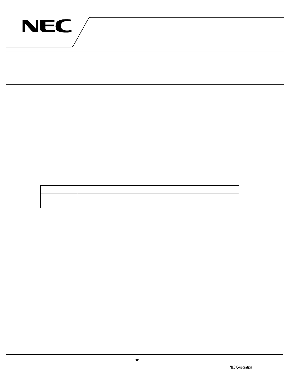
INTERNAL BLOCK DIAGRAM AND PIN CONFIGURATION (Top View)
µµµµ
PC2798GR
AGC IN1
AGC IN2
AGC
V
VCC1
OSC OUT
GND
OSC B2
OSC C1
OSC C2
OSC B1
1
2
3
4
5
6
7
8
9
10
AGC Amp
OSC OUT
Buffer Amp
OSC
MIXER
OSC Buffer
Amp
VIDEO
Amp
20
19
18
17
16
15
14
13
12
11
GND
MIX OUT2
MIX OUT1
G1A
G1B
INA
INB
CC
2
V
OUT1
OUT2
2
Data Sheet P11998EJ3V0DS00
Page 3
PIN EXPLANATIONS
1
4
2
AGC
control
Reg
3
4
AGC
control
10
948
7
Reg
Reg
µµµµ
PC2798GR
Pin No. Symbol
1 AGC IN1 1.5 Input pin of IF signal.
2 AGC IN2 1.5
3V
4 Vcc1 5.0 Power supply pin of IF down convertor block.
5OSC
AGC
OUT
Pin Voltage
(V, TYP.)
0 to 5
4.0
Explanation Equivalent Circuit
1pin is same phase and 2pin is oppos i te
phase at balance input.
In case of single input, 1pin or 2pin should
be grounded through capacitor.
Automatic gain control pi n.
This pin’s bias govern the A G C out put level.
AGC
AGC
= 0 V
= 5 V
Minimum gain at V
Maximum gain at V
Recommend to use by deviding AGC voltage
with externally resis tor (ex. 100 kΩ).
Must be connected bypass capacitor to
minimize ground impedance.
Output pin of Oscillator frequency.
Connected to PLL symthesizer IC’s input pin.
4
6 GND 0.0 Ground pin.
7 OSC B2
8OSC C1
9OSC C2
10 OSC B1
2.4
4.6
4.6
2.4
Must be connected to the system ground
with minimum inductanc e.
Ground pattern on the board should be
formed as wide as possible.
Internal oscillator consist in balance amplifier.
7 and 8pins, 9 and 10 pins should be
externally connected to oscillate wit h active
feedback loop.
Connected LC resonator between 7pin and
10pin.
Data Sheet P11998EJ3V0DS00
5
Reg
3
Page 4
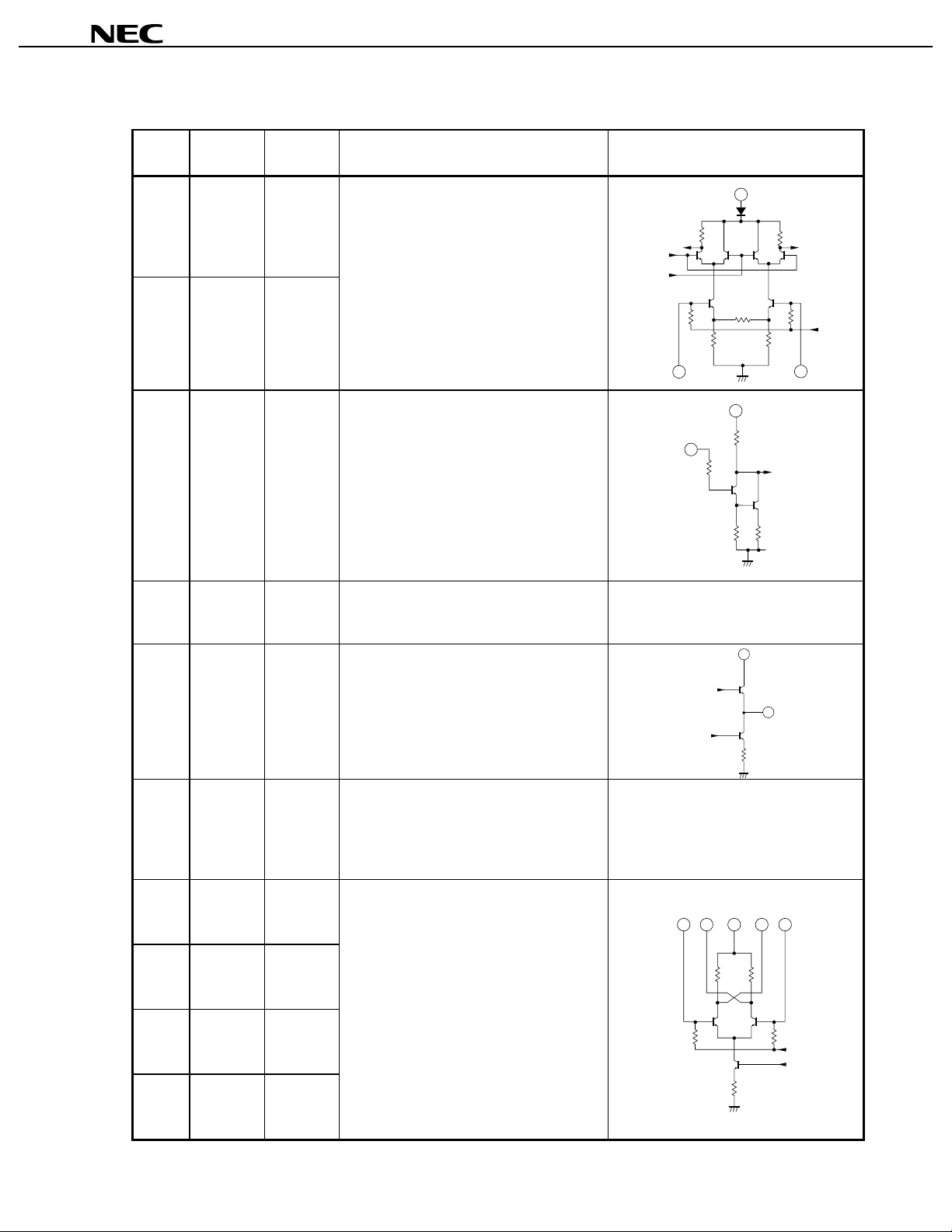
PIN EXPLANATIONS
12
11
13
REG
Pin No. Symbol
Pin Voltage
(V, TYP.)
( ) is
value at
Vcc2 = 9 V.
Explanation Equivalent Circuit
µµµµ
PC2798GR
11 OUT2 2.5
(4.7)
Output pin of video amplifi er.
L
In case of R
voltage equal 3 V
= 1 kΩ, differential output
P-P
.
OUT1 and INA are same phase.
OUT2 and INB are same phase.
11 OUT1 2.5
(4.7)
13 Vcc2 5 to 9 Power supply pi n of video amplifier.
Must be connected bypass capacitor to
minimize ground impedance.
14 INB
15 INA
2.5
(4.1)
2.5
Signal input pin of video ampl i f i er.
This pin is high impedance.
(4.1)
16 G1B 1.7
(3.3)
Gain control pin of video ampli fier.
Maximum gain at G1A-GIB = short .
Minimum gain at G1A-G1B = open.
Gain is able to adjust by i ns erting arbitrary
resistor between 16pin and 17pin.
17 G1A
1.7
(3.3)
17
REG
15
13
14 16
18 MIX
19 MIX
20 GND
4
4
OUT1
3.7 Output pin of mixer.
This output pin features low-i m pedance
because of its emitter-follower output port.
18
3.7
REG
19
OUT2
0.0
Ground pin.
Must be connected to the system ground
with minimum inductanc e.
Ground pattern on the board should be
formed as wide as possible.
Data Sheet P11998EJ3V0DS00
Page 5
µµµµ
PC2798GR
ABSOLUTE MAXIMUM RATINGS (TA = 25
C unless otherwise specified)
°°°°
PARAMETER SYMBOL RATING UNIT TEST CONDITIONS
Supply Voltage 1 Vcc1 6.0 V Mixer block
Supply Voltage 2 Vcc2 6.0 V Video Amp block
Power Dissipation P
Operating Ambient Temperature T
Storage Temperature T
A
D
A
stg
430 mW
40 to +85
−
55 to +150
−
T
C
°
C
°
= 85 °C
*1
PARAMETER SYMBOL RATING UNIT TEST CONDITIONS
Supply Voltage 1 Vcc1 6.0 V Mixer block
Supply Voltage 2 Vcc2 11.0 V Video Amp block
Power Dissipation P
Operating Ambient Temperature T
Storage Temperature T
Mounted on 50 × 50 × 1.6 mm double copper epoxy glass board.
*1.
D
A
stg
500 mW
40 to +75
−
55 to +150
−
A
T
C
°
C
°
= 75 °C
*1
RECOMMENDED OPERATING RANGE
PARAMETER SYMBOL MIN. TYP. MAX. UNIT
Supply Voltage 1 Vcc1 4.5 5.0 5.5 V
Supply Voltage 2 Vcc2 4.5 5. 0 10.0 V
Operating Ambient Temperature 1
Operating Ambient Temperature 2
@Vcc1 = Vcc2 = 4.5 to 5.5 V
*2.
@Vcc1 = 4.5 to 5.5 V, Vcc2 = 4.5 to 10.0 V
*3.
ELECTRICAL CHARACTERISTICS (T
*2
*3
A
= 25
TA1
TA2
40 +25 +85
−
40 +25 +75
−
C)
°°°°
C
°
C
°
PARAMETER SYMBOL MIN. TYP. MAX. UNIT TEST CONDITIONS
Total Block (RL = 1 kΩ, by measurement circ ui t 5)
Circuit Current 1 Icc1 24.0 35.5 45.0 mA no i nput signal, Vcc1 = Vc c 2 = 5 V
AGC
V
Maximum Conversion Gain 1 CG
Maximum Conversion Gain 2 CG
Minimum Conversion Gain 1 CG
Minimum Conversion Gain 2 CG
MAX
1 68.0 74.0 76.0 dB
MAX
2
MIN
1 32.0 39.0 43.0 dB
MIN
2
58.0
22.0
dB
dB
= 4.0 V, G1A-G1B pins: s hort
AGC
V
= 4.0 V, G1A-G1B pins: open
AGC
V
= 1.0 V, G1A-G1B pins: s hort
AGC
V
= 1.0 V, G1A-G1B pins: open
Circuit Current 2 Icc1 32.0 47.0 60.0 mA no i nput signal, Vcc1 = 5 V, Vcc2 = 9 V
AGC
V
Maximum Conversion Gain 3 CG
Maximum Conversion Gain 4 CG
Minimum Conversion Gain 3 CG
Minimum Conversion Gain 4 CG
MAX
3 72.0 78.5 81.0 dB
MAX
MIN
MIN
4
3
4
59.0
43.5
22.5
dB
dB
dB
= 4.0 V, G1A-G1B pins: s hort
AGC
V
= 4.0 V, G1A-G1B pins: open
AGC
V
= 1.0 V, G1A-G1B pins: s hort
AGC
V
= 1.0 V, G1A-G1B pins: open
*4
*4
*4
*4
*4
*4
*4
*4
Data Sheet P11998EJ3V0DS00
5
Page 6
µµµµ
PC2798GR
ELECTRICAL CHARACTERISTICS (TA = 25
C)
°°°°
PARAMETER SYMBOL MIN. TYP. MAX. UNIT TEST CONDITIONS
AGC Amplifier + Mixer Block (@Vcc1 = 5 V, RL = 50 Ω, by measurement circ ui t 1)
Circuit Current 3 Icc3 15.0 23.0 28.0 mA no i nput signal
RF Input Frequency Range f
OSC Frequency Range f
IF Output Frequency Range f
Minimum Conversion Gain 5 CG
Minimum Conversion Gain 5 CG
AGC Dynamic Range GCR 26 32
Noise Figure NF
AGC Voltage High Level V
AGC Voltage Low Level V
RF
OSC
IF
MAX
MIN
30
30
DC
5
5
−
AGC
H4.0
AGC
L
25
7
250 Mhz
250 Mhz
150 Mhz
9
1.0 V @Minimum Gain
dB
dB
dB V
dB
AGC
V
AGC
V
AGC
SSB, V
*4
= 4.0 V
*4
= 1.0 V
= 1.0 to 4.0 V
AGC
= 4.0 V (@Maximum Gain)
V @Maximum Gain
Video Amp. Block (@Vc c2 = 5 V, RL = 1 kΩ, Input: 51 Ω terminated, by measurement circuit 3)
Circuit Current 4 Icc4 9.0 12.5 17.0 mA no input si gnal
Differential Gain 1 G1
200
V/V G1A-G1B pins: short, Vout = 3.0 V
fin = 10 MHz
Differential Gain 2 G2
26.0
V/V G1A-G1B pins: open, Vout = 3.0 V
fin = 10 MHz
Video Amp. Block (@Vc c2 = 9 V, RL = 1 kΩ, Input: 51 Ω terminated, by measurement circuit 3)
Circuit Current 5 Icc5 17.0 24.0 32.0 mA no i nput signal
Differential Gain 3 G3
385
V/V G1A-G1B pins: short, Vout = 3.0 V
fin = 10 MHz
Differential Gain 4 G4
28.5
V/V G1A-G1B pins: open, Vout = 3.0 V
fin = 10 MHz
Video Amp. Block (@V cc2 = 5 V or 9 V: Common, RL = 1 kΩ, Input: 51 Ω terminated, by measurement circuit 3)
Output Voltage V
OUT
Bandwidth 1 BW
Bandwidth 2 BW
Input Resistance 1 Rin1
Input Resistance 2 Rin2
Input Capacitance Cin
G1
G2
3.0
50
50
3.5
9.7
1.6
P-P
V
RL = 1 kΩ, differential
MHz G1 (G1A-G1B pi ns: short)
MHz G2 (G1A-G1B pi ns: open)
k
G1 (G1A-G1B pins: short)
Ω
k
G2 (G1A-G1B pins: open)
Ω
pF
P-P
P-P
P-P
P-P
*4, 5
,
,
,
,
RF
= 45 MHz, f
.f
*4
. By measurement circuit 2
*5
6
OSC
= 55 MHz, P
OSC
= −10 dBm
Data Sheet P11998EJ3V0DS00
Page 7
µµµµ
PC2798GR
STANDARD CHARACTERISTICS (TA = 25
PARAMETER SYMBOL
C)
°°°°
VALUE FOR
REFERENCE
UNIT TEST CONDITIONS
AGC Amplifier + Mixer B l ock (@Vcc1 = 5 V, by measurement circuit 1)
AGC
= 1.0 V @Minimum Gain
AGC Input Intercept Poi nt 1 AGC
IIP
9dBm
−
3
1
V
Video Amp. Block (RL = 50 Ω, input: 51 Ω terminated, by measurement circuit 4)
Single-end Gain 1 AVS1 40.0 dB VCC2 = 5 V, G1A-G1B pins: short
Single-end Gain 2 AVS2 22.5 dB VCC2 = 5 V, G1A-G1B pins: open
Single-end Gain 3 AVS3 45.0 dB VCC2 = 9 V, G1A-G1B pins: short
Single-end Gain 4 AVS4 23.5 dB VCC2 = 9 V, G1A-G1B pins: open
Input Intercept Point 2 IIP32
11.5 dBm VCC2 = 5 V, G1A-G1B pins: open
−
fin1 = 9 MHz, fin2 = 11 MHz
Input Intercept Point 3 IIP33
5.0 dB m VCC2 = 9 V, G1A-G1B pins: open
−
fin1 = 9 MHz, fin2 = 11 MHz
Video Amp. Block (@V cc2 = 5 V or 9 V: Common, by m eas urement circuit 3)
Common Mode Rejection
CMRR 80 dB VCM = 1 V
P-P
, f = 100 kHz
Ratio
Power Supply Rejection
PSRR 70 dB
Ratio
Rise Time
Propagation Delay Time
R
τ
PD
τ
2.6 ns
4.4 ns
Total Block (RL = 1 kΩ, by measurement circ ui t 5)
Input Intercept Point 4 IIP34
14.0 dBm VCC1 = VCC2 = 5 V, V
−
AGC
= 1 V,
G1A-G1B pins: short
Input Intercept Point 5 IIP35
8.0 dB m VCC1 = VCC2 = 5 V, V
−
AGC
= 1 V,
G1A-G1B pins: open
Input Intercept Point 6 IIP36
7.5 dB m VCC1 = 5 V, VCC2 = 9 V, V
−
AGC
G1A-G1B pins: open
*6
*6
*6
= 1 V,
*6
RF
1 = 44 MHz, fRF2 = 46 MHz, f
f
*6
OSC
= 55 MHz, P
Data Sheet P11998EJ3V0DS00
OSC
= −10 dBm
7
Page 8
TYPICAL CHARACTERISTICS
(by measurement circuit 5, TA = 25 °C, f
OSC
= fRF + 10 MHz, P
OSC
=
−−−−
10 dBm)
µµµµ
PC2798GR
CONVERSION GAIN vs. INPUT FREQUENCY
80
V
AGC
= 4 V
60
V
AGC
= 3 V
40
V
AGC
= 1 V
20
CG - Conversion Gain - dB
V
CC
1 = 5 V
CC
2 = 5 V
V
1 kΩ Load
G1A–G1B: short
0
0 50 100 150 200 250
fRF - Input Freqency - MHz
CONVERSION GAIN vs. INPUT FREQUENCY
80
V
AGC
= 4 V
AGC
= 3 V
V
60
AGC
= 1 V
V
40
20
CG - Conversion Gain - dB
V
CC
1 = 5 V
CC
2 = 9 V
V
1 kΩ Load
G1A–G1B: short
0
0 50 100 150 200 250
fRF - Input Frequency - MHz
CONVERSION GAIN vs. INPUT FREQUENCY CONVERSION GAIN vs. INPUT FREQUENCY
80
80
V
AGC
60
40
20
CG - Conversion Gain - dB
= 4 V
AGC
= 3 V
V
AGC
= 1 V
V
VCC1 = 5 V, VCC2 = 5 V
G1A–G1B: open
1 kΩ load
0
0 50 100 150 200 250
fRF - Input Frequency - MHz
V
AGC
60
40
20
CG - Conversion Gain - dB
= 4 V
AGC
= 3 V
V
AGC
= 1 V
V
VCC1 = 5 V, VCC2 = 9 V
G1A–G1B: open
1 kΩ load
0
0 50 100 150 200 250
fRF - Input Frequency - MHz
8
Data Sheet P11998EJ3V0DS00
Page 9

µµµµ
PC2798GR
TYPICAL CHARACTERISTICS
(by measurement circuit 5, TA = 25 °C, fRF = 45 MHz, P
CONVERSION GAIN vs. INTERMEDIATE FREQUENCY CONVERSION GAIN vs. INTERMEDIATE FREQUENCY
80
60
40
20
CG - Conversion Gain - dB
V
VCC1 = 5 V, VCC2 = 5 V
G1A–G1B: short
1 kΩ load
0
0 40 80 120 160
fIF - Intermediate Frequency - MHz
AGC
AGC
V
= 1 V
V
AGC
= 3 V
= 4 V
OSC
=
10 dBm)
−−−−
80
60
40
20
CG - Conversion Gain - dB
VCC1 = 5 V, VCC2 = 9 V
G1A–G1B: short
1 kΩ load
0
0 40 80 120 160
fIF - Intermediate Frequency - MHz
V
AGC
= 4 V
AGC
= 3 V
V
AGC
= 1 V
V
CONVERSION GAIN vs. INTERMEDIATE FREQUENCY CONVERSION GAIN vs. INTERMEDIATE FREQUENCY
80
60
V
AGC
40
20
CG - Conversion Gain - dB
= 4 V
AGC
= 3 V
V
VCC1 = 5 V, VCC2 = 5 V
G1A–G1B: open
1 kΩ load
0
0 40 80 120 160
fIF - Intermediate Frequency - MHz
80
60
V
AGC
40
20
CG - Conversion Gain - dB
= 4 V
AGC
= 3 V
V
VCC1 = 5 V, VCC2 = 9 V
G1A–G1B: open
1 kΩ load
0
0 40 80 120 160
fIF - Intermediate Frequency - MHz
Data Sheet P11998EJ3V0DS00
9
Page 10

TYPICAL CHARACTERISTICS (by measurement circuit 1, TA = 25 °C)
µµµµ
PC2798GR
CIRCUIT CURRENT vs. SUPPLY VOLTAGE
50
no input
signal
AGC
= 0 V
V
40
30
20
- Circuit Current - mA
CC
I
10
0
024681012
V
CC
- Supply Voltage - V
Total
Mixer
+ AGC + VCO
Video Amp
CONVERSION GAIN vs. INTERMEDIATE FREQUENCY
30
AGC
= 4.0 V
20
V
10
CONVERSION GAIN vs. INPUT FREQUENCY
30
AGC
20
V
10
V
AGC
0
–10
V
AGC
CG - Conversion Gain - dB
–20
f
OSC
= f
RF
P
OSC
= –10 dBm
CC1 = 5 V
V
–30
0 50 100 150 200 250 300
f
+ 10 MH
Z
RF
- Input Frequency - MHz
NOISE FIGURE vs. AGC VOLTAGE
30
20
= 4.0 V
= 2.6 V
= 0.0 V
V
AGC
= 2.6 V
0
–10
fRF = 45 MH
CG - Conversion Gain - dBCG - Conversion Gain - dB
f
OSC
–20
P
OSC
CC1 = 5 V
V
–30
0 30 60 90 120 150 180 0 1 2 3 4 5
Z
= 55 to 210 MH
Z
= –10 dBm
IF
- Intermediate Frequency - MHz V
f
V
AGC
= 0.0 V
CONVERSION GAIN vs. AGC VOLTAGE
30
V
CC1 = 5 V
RF
= 45 MH
f
Z
PRF = –60 dBm
OSC
20
f
P
OSC
= 50 MH
Z
= –10 dBm
10
10
NF - Noise Figure - dB
V
CC1 = 5 V
RF
= 100 MH
f
f
OSC
= 120 MH
P
OSC
Z
= –10 dBm
DSB mode
0
OUTPUT POWER vs. INPUT POWER
–10
V
CC1 = 5 V
AGC
= 0 V
V
–20
RF
–30
–40
1 = 44 MH
f
fRF2 = 46 MH
f
OSC
= 55 MH
P
OSC
= –10 dBm
Z
Z
Z
–50
Z
AGC
- AGC Voltage - V
–60
- Output Power - dBm
out
0
P
–70
–80
10
–10
012345
AGC
- AGC Voltage - V
V
Data Sheet P11998EJ3V0DS00
–90
–60 –50 –40 –30 –20 –10 0
Pin - Input Power - dBm
Page 11

STANDARD CHARACTERISTICS (by measurement circuit 3, TA = 25 °C)
µµµµ
PC2798GR
DIFFERENTIAL GAIN vs. INPUT FREQUENCY
400
VCC2 = 9 V
300
200
CC2 = 5 V
V
100
GVIDEO - Differential Gain - V/V
G1A–G1B: short
P
OUT = 1.5 Vp–p const.
0
0 20406080100
fin - Input Frequency - MHz
OUTPUT POWER vs. INPUT POWER
0
V
CC2 = 9 V
–10
CC2 = 5 V
V
DIFFERENTIAL GAIN vs. INPUT FREQUENCY
40
30
20
10
GVIDEO - Differential Gain - V/V
CC2 = 5 V
V
VCC2 = 9 V
G1A–G1B: open
P
OUT = 1.5 Vp–p const.
0
0 20406080100
fin - Input Frequency - MHz
OUTPUT POWER vs. INPUT POWER
0
V
–10
CC2 = 9 V
–20
V
CC2 = 5 V
–20
Pout - Output Power (50 Ω/1 kΩ) - dBm
fin = 10 MHz
G1A–G1B: short
–30
–40 –30 –20 –10 0
Pin - Input Power (50 Ω) - dBm
DIFFERENTIAL GAIN vs. EXTERNAL RESISTANCE
500
fin =10 MHz
400
300
V
200
CC2 = 5 V
V
100
GVIDEO - Differential Gain - V/V
CC2 = 9 V
0
short 30 43 56 100 246 2000 open
Resistance - Ω
–30
–40
Pout - Output Power (50 Ω/1 kΩ) - dBm
fin = 10 MHz
G1A–G1B: open
–50
–40 –30 –20 10 100
Pin - Input Power (50 Ω) - dBm
Data Sheet P11998EJ3V0DS00
11
Page 12

STANDARD CHARACTERISTICS (by measurement circuit 4, TA = 25 °C)
µµµµ
PC2798GR
50
GAIN vs. INPUT FREQUENCY
40
30
- Gain - dB
20
VS
A
10
VCC2 = 5 V
G1A–G1B: short
0
0.1 1 10 100
Input Frequency fin - MHz
GAIN vs. INPUT FREQUENCY
50
40
50
GAIN vs. INPUT FREQUENCY
40
30
- Gain - dB
20
VS
A
10
VCC2 = 5 V
G1A–G1B: open
0
0.1 1 10 100
Input Frequency fin - MHz
GAIN vs. INPUT FREQUENCY
50
40
30
- Gain - dB
VS
20
A
10
VCC2 = 9 V
G1A–G1B: short
0
0.1 1 10 100
Input Frequency fin - MHz
OUTPUT POWER vs. INPUT POWER
20
0
–20
–40
–60
Pout - Output Power (50 Ω)/tone - dBm
–80
–50 –40 –30 –20 –10
VCC2 = 5 V
f1 = 9 MHz
2
= 11 MHz
f
G1A–G1B: open
Pin - Input Power (50 Ω)/tone - dBm
30
- Gain - dB
VS
20
A
10
VCC2 = 9 V
G1A–G1B: open
0
0.1 1 10 100
Input Frequency fin - MHz
OUTPUT POWER vs. INPUT POWER
20
0
–20
–40
–60
Pout - Output Power (50 Ω)/tone - dBm
–80
–50 –40 –30 –20 –10
VCC2 = 9 V
f1 = 9 MHz
2
= 11 MHz
f
G1A–G1B: open
Pin - Input Power (50 Ω)/tone - dBm
12
Data Sheet P11998EJ3V0DS00
Page 13

STANDARD CHARACTERISTICS (by measurement circuit 5)
µµµµ
PC2798GR
OUTPUT POWER vs. INPUT POWER
0
–20
–40
CC
1 = 5 V
V
V
CC
–60
Pout - Output Power (50 Ω/1 kΩ)/tone - dBm
–80
–50 –40 –30 –20 –10 0
2 = 5 V
f1 = 44 MHz
f2 = 46 MHz
f
OSC =
55 MHz
P
OSC =
–10 dBm
G1A–G1B: open
OUTPUT POWER vs. INPUT POWER
0
–20
OUTPUT POWER vs. INPUT POWER
0
–20
–40
CC
1 = 5 V
V
–60
Pout - Power Pout (50 Ω/1 kΩ)/tone - dBm
–80
–50 –40 –30 –20 –10 0
VCC2 = 9 V
f
1 =
44 MHz
f2 = 46 MHz
f
OSC =
55 MHz
P
OSC =
–10 dBm
G1A–G1B: open
Pin - Input Power (50 Ω)/tone - dBmPin - Input Power (50 Ω)/tone - dBm
–40
CC
1 = 5 V
V
–60
Pout - Output Power (50 Ω/1 kΩ)/tone - dBm
–80
–50 –40 –30 –20 –10 0
VCC2 = 5 V
f
1 =
44 MHz
f2 = 46 MHz
f
OSC =
55 MHz
P
OSC =
–10 dBm
G1A–G1B: short
Pin - Input Power (50 Ω)/tone - dBm
Data Sheet P11998EJ3V0DS00
13
Page 14

STANDARD CHARACTERISTICS
(by application circuit example: MIXER block, T
A
= 25 °C)
µµµµ
PC2798GR
CONVERSION GAIN vs. INPUT FREQUENCY
30
V
CC
1 = 5.5 V
V
CC
25
CC
V
1 = 5.0 V
1 = 4.5 V
CG - Conversion Gain - dB
f
RF
= 50 MHz
IF
= 10 MHz
f
RF
=
–50 dBm
P
V
AGC =
20
4 V
30 40 50 60
RF
- Input Frequency - MHz
f
CONVERSION GAIN vs. AGC VOLTAGE
30
f
RF
= 50 MHz
IF
= 10 MHz
f
RF
= –50 dBm
P
CC
1 = 4.5 V
V
20
V
V
CC
1 = 5.0 V
CC
1 = 5.5 V
30
NOISE FIGURE vs. AGC VOLTAGE
20
10
NF - Noise Figure - dB
f
RF
= 50 MHz
IF
= 10 MHz
f
CC
1 = 4.5 V
V
CC
1 = 5.0 V
V
CC
1 = 5.5 V
V
DSB
0
012345
V
AGC
- AGC Voltage - V
OUTPUT POWER vs. INPUT POWER
–10
–20
–30
–40
10
0
CG - Conversion Gain - dB
–10
0
12345
V
AGC
- AGC Voltage - V
OSCILLATOR FREQUENCY vs. TUNING VOLTAGE
70
60
50
40
- Oscillator Frequency - MHz
OSC
f
–50
–60
–70
Pout - Output Power - dBm
–80
–90
–100
–50 –40 –30 –20 –10 0 10
–60
Pin - Input Power - dBm
VCC1 = 5 V
RF1
= 45 MHz
f
RF2
= 46 MHz
f
OSC
= 55 MHz
f
AGC
= 0 V
V
14
30
VCC1 = 5 V
0
5101520
Vtu - Tuning Voltage - V
Data Sheet P11998EJ3V0DS00
Page 15

MEASUREMENT CIRCUIT 1
<AGC + MIX block>
µµµµ
PC2798GR
10 nF
IN
V
VCC1
OSC OUT
OSC IN
AGC
220 nF
1 nF
100 k
10 nF
10 nF
MEASUREMENT CIRCUIT 2
10 nF
220 nF
10 nF
100 k
1
2
3
4
5
6
7
8
9
10
AGC Amp
OSC OUT
Buffer Amp
OSC
MIXER
OSC Buffer
Amp
VIDEO
Amp
20
19
18
17
16
15
14
13
12
11
10 nF MIX OUT
10 nF
50 Ω
<AGC + MIX block>
Noise Source
10 nF
BPF
V
AGC
220 nF
VCC1
1 nF
50 Ω
SG1
(50 Ω)
10 nF
100 k
10 nF
10 nF
220 nF
10 nF
100 k
1
2
3
4
5
6
7
8
9
10
AGC Amp
OSC OUT
Buffer Amp
OSC
NF METER
MIXER
VIDEO
Amp
OSC Buffer
Amp
20
19
18
17
16
15
14
13
12
11
BPF
10 nF
10 nF
50 Ω
Data Sheet P11998EJ3V0DS00
15
Page 16

MEASUREMENT CIRCUIT 3
<Video Amp. block>
µµµµ
PC2798GR
AGC Amp
1
2
3
OSC OUT
4
Buffer Amp
5
6
7
8
9
10
MEASUREMENT CIRCUIT 4
OSC
MIXER
OSC Buffer
Amp
VIDEO
Amp
20
19
18
17
16
15
14
13
12
11
open
/short
10 nF
10 nF
1 nF
10 nF
10 nF
51 Ω
51 Ω
220 nF
1 kΩ
SG or
Network
Analyzer
(50 Ω)
50 Ω
VCC 2
950 Ω
(50 Ω)
Spectrum Analyzer or
Network Analyzer or
Oscilloscope
<Video Amp. block>
AGC Amp
1
2
3
OSC OUT
4
Buffer Amp
5
6
7
8
9
10
In case of measurement of IIP3
*7:
OSC
MIXER
OSC Buffer
Amp
VIDEO
Amp
20
19
18
17
16
15
14
13
12
11
open
/short
10 nF
10 nF
1 nF
10 nF
10 nF
51 Ω
51 Ω
SG1
(50 Ω)
220 nF
50 Ω
50 Ω
*7
MIX PAD
VCC 2
SG2
(50 Ω)
Spectrum
Analyzer
(50 Ω)
16
Data Sheet P11998EJ3V0DS00
Page 17

MEASUREMENT CIRCUIT 5
<Total block>
µµµµ
PC2798GR
*8
SG3
(50 Ω)
MIX PAD
V
VCC1
OSC OUT
(50 Ω)
AGC
SG2
SG1
(50 Ω)
220 nF
1 nF
10 nF
100 k
10 nF
10 nF
10 nF
220 nF
10 nF
100 k
1
2
3
4
5
6
7
8
9
10
AGC Amp
OSC OUT
Buffer Amp
OSC
MIXER
OSC Buffer
Amp
VIDEO
Amp
20
19
18
17
16
15
14
13
12
11
open
/short
10 nF
1 nF
10 nF
10 nF
220 nF
1 kΩ
1 k1 k
5 pF
10 nF
950 Ω
VCC 2
Spectrum
Analyzer
(50 Ω)
: In case of measurement of IIP3
*8
Data Sheet P11998EJ3V0DS00
17
Page 18

APPLICATION CIRCUIT EXAMPLE
µµµµ
PC2798GR
10 nF
IN
10 nF
100 k
100 k
220 nF
10 nF
1000 pF
10 pF
20 pF
10 pF
1000 pF
OSC OUT
Vtu
V
VCC1
10 k
CV
1.0 H
AGC
220 nF
1 nF
µ
10 k
CV: N ratio = 10 to 11 (ex. HVU 200 A)
1
2
3
4
5
6
7
8
9
10
AGC Amp
OSC OUT
Buffer Amp
OSC
MIXER
OSC Buffer
Amp
VIDEO
Amp
20
19
18
17
16
15
14
13
12
11
open
/short
10 nF
1 nF
10 nF
10 nF
220 nF
1 k1 k
5 pF
10 nF
VCC 2
OUT 1
OUT 2
The application circuits and their parameters are for reference only and are not intended for use in actual design-ins.
18
Data Sheet P11998EJ3V0DS00
Page 19

ILLUSTRATION OF THE APPLICATION CIRCUIT ASSEMBLED ON EVALUATION BOARD
VCC2
µµµµ
PC2798GR
MIX
OUT 1
VIDEO
IN 1
MIX
OUT 2
VIDEO
IN 2
AGC IN
10 n
10 n
5 p
1 k
10 n
1 k
100 k
220 n
10 n
100 k
R
10 p
1 n 220 n
1 n
220 n
10 k
1000 p
10 p
20 p
Cv
1000 p
PC2798GR
µ
VIDEO
OUT 1
10 n
10 n
VIDEO
µ
1.2
Cv
10 k
10 n
OUT 2
OSC OUT
V
tu
Notes
*1)
*2)
*3)
*4)
V
AGCVCC
1
R is resistance to control video amplifier gain. (short to open)
V
is variable capacitor. (N ratio = 10 to 11, Example: HVU200A)
C
shows through holes
pattern should be removed on this application
Data Sheet P11998EJ3V0DS00
19
Page 20

PACKAGE DIMENSIONS
20 PIN PLASTIC SSOP (225 mil) (UNIT: mm)
µµµµ
PC2798GR
20
110
6.7 ± 0.3
1.8 MAX.
1.5 ± 0.1
11
detail of lead end
3˚
6.4 ± 0.2
4.4 ± 0.1
+7˚
–3˚
1.0 ± 0.2
NOTE
0.5 ± 0.2
0.15
+0.10
–0.05
0.1 ± 0.1
0.65
0.22
+0.10
–0.05
0.10
0.15
M
0.575 MAX.
Each lead centerline is located within 0.10 mm of its true position (T.P.) at maximum material condition.
20
Data Sheet P11998EJ3V0DS00
Page 21

µµµµ
PC2798GR
RECOMMENDED SOLDERING CONDITIONS
The following conditions (see table below) must be met when soldering this product.
Please consult with our sales officers in case other soldering process is used or in case soldering is done under
different conditions.
For details of recommended soldering conditions for surface mounting, refer to information document
SEMICONDUCTOR DEVICE MOUNTING TECHNOLOGY MANUAL (C10535E).
PC2798GR
µµµµ
Soldering process Soldering conditions Symbol
Infrared ray reflow Peak package’s surface temperat ure: 235 °C or below,
Reflow time: 30 seconds or bel ow (210 °C or higher),
Number of reflow process: 3, Exposure limit
VPS Peak package’s surface temperature: 215 °C or below,
Reflow time: 40 seconds or bel ow (200 °C or higher),
Number of reflow process: 3, Exposure limit
Partial heating method Terminal temperat ure: 300 °C or below,
Note
Flow time: 3 seconds or below,
Exposure limit
Exposure limit before soldering after dry-pack package is opened.
Note
: None
Note
Note
: None
: None
Storage conditions: 25 °C and relative humidity at 65% or less.
Caution Do not apply more than single process at once, except for “Partial heating method”.
IR35-00-3
VP15-00-3
Data Sheet P11998EJ3V0DS00
21
Page 22

[MEMO]
µµµµ
PC2798GR
22
Data Sheet P11998EJ3V0DS00
Page 23

[MEMO]
µµµµ
PC2798GR
Data Sheet P11998EJ3V0DS00
23
Page 24

µµµµ
PC2798GR
NESAT (NEC Silicon Advanced Technology) is trademark of NEC Corporation.
• The information in this document is subject to change without notice. Before using this document, please
confirm that this is the latest version.
• No part of this document may be copied or reproduced in any form or by any means without the prior written
consent of NEC Corporation. NEC Corporation assumes no responsibility for any errors which may appear in
this document.
• NEC Corporation does not assume any liability for infringement of patents, copyrights or other intellectual property
rights of third parties by or arising from use of a device described herein or any other liability arising from use
of such device. No license, either express, implied or otherwise, is granted under any patents, copyrights or other
intellectual property rights of NEC Corporation or others.
• Descriptions of circuits, software, and other related information in this document are provided for illustrative
purposes in semiconductor product operation and application examples. The incorporation of these circuits,
software, and information in the design of the customer's equipment shall be done under the full responsibility
of the customer. NEC Corporation assumes no responsibility for any losses incurred by the customer or third
parties arising from the use of these circuits, software, and information.
• While NEC Corporation has been making continuous effort to enhance the reliability of its semiconductor devices,
the possibility of defects cannot be eliminated entirely. To minimize risks of damage or injury to persons or
property arising from a defect in an NEC semiconductor device, customers must incorporate sufficient safety
measures in its design, such as redundancy, fire-containment, and anti-failure features.
• NEC devices are classified into the following three quality grades:
"Standard", "Special", and "Specific". The Specific quality grade applies only to devices developed based on a
customer designated "quality assurance program" for a specific application. The recommended applications of
a device depend on its quality grade, as indicated below. Customers must check the quality grade of each device
before using it in a particular application.
Standard: Computers, office equipment, communications equipment, test and measurement equipment,
audio and visual equipment, home electronic appliances, machine tools, personal electronic
equipment and industrial robots
Special: Transportation equipment (automobiles, trains, ships, etc.), traffic control systems, anti-disaster
systems, anti-crime systems, safety equipment and medical equipment (not specifically designed
for life support)
Specific: Aircraft, aerospace equipment, submersible repeaters, nuclear reactor control systems, life
support systems or medical equipment for life support, etc.
The quality grade of NEC devices is "Standard" unless otherwise specified in NEC's Data Sheets or Data Books.
If customers intend to use NEC devices for applications other than those specified for Standard quality grade,
they should contact an NEC sales representative in advance.
M7 98. 8
 Loading...