

Page 1
DATA SHEET
BIPOLAR ANALOG INTEGRATED CI RCUITS
µµµµ
PC2791TB,
µµµµ
PC2792TB
5 V, SUPER MINIMOLD SILICON MMIC
VHF-UHF WIDEBAND AMPLIFIER
DESCRIPTION
The µPC2791TB and µPC2792TB are silicon monolithic integrated circuits designed as 2nd IF buffer amplifier for
DBS tuners. These ICs are packaged in super minimold package which is smaller than conventional minimold. So,
in the case of reducing your system size, µPC2791TB and µPC2792TB are suitable. Among the 6-pin mini/superminimold amplifiers, µPC2791TB and µPC2792TB have unique pin locations taken over from conventional 4-pin
minimold µPC1675G, µPC1676G and µPC1688G.
These ICs are manufactured using NEC’s 10GHz fT NESAT™ II AL silicon bipolar process. This process uses
silicon nitride passivation film. The material can protect chip surface from external pollution and prevent
corrosion/migration. Thus, these IC have excellent performance, uniformity and reliability.
FEATURES
• High-density surface mounting : 6-pin super minimold package (2.0 × 1.25 × 0.9 mm)
• Supply voltage : VCC = 4.5 to 5.5 V
• Wideband response :µPC2791TB; fu = 1.9 GHz TYP. @3 dB bandwidth
PC2792TB; fu = 1.2 GHz TYP. @3 dB bandwidth
µ
• Power gain :µPC2791TB; GP = 12 dB TYP. @f = 500 MHz
PC2792TB; GP = 22 dB TYP. @f = 500 MHz
µ
APPLICATION
• 400 MHz band 2nd IF buffer amplifiers in DBS tuners (2nd frequecy converter block), etc.
ORDERING INFORMATION
Part Number Package Marking Supplying Form
µ
PC2791TB-E3 C2S
µ
PC2792TB-E3
Remark
To order evaluation samples, please contact your local NEC sales office. (Part number for sample
order:
The information in this document is subject to change without notice. Before using this document, please
confirm that this is the latest version.
Not all devices/types available in every country. Please check with local NEC representative for
availability and additional information.
6-pin super minimold
PC2791TB, µPC2792TB)
µ
Caution Electro-static sensitive devices
C2T
Embossed tape 8 mm wide.
1, 2, 3 pins face to perforat i on side of the tape.
Qty 3kpcs/reel.
Document No. P11863EJ2V0DS00 (2nd edition)
Date Published February 2000 N CP(K)
Printed in Japan
The mark shows major revised points.
©
1996, 2000
Page 2
,
PIN CONNECTIONS
µµµµ
PC2791TB
µµµµ
PC2792TB
Caution
(Top View)
3
2
1
4
5
6
C2S
Marking is an example of µPC2791TB
PC2791TB,
µµµµ
PC2792TB pin locations are different from the other 6-pin mini/super-minimold
µµµµ
(Bottom View)
4
5
6
Pin No. Pin Name
3
2
1
1GND
2GND
3OUTPUT
4V
5GND
6 INPUT
amplifiers.
PRODUCT LINE-UP (TA = +25
u
Part Number
PC1675G 1.9 +4.0 12 5.5 17 4-pin minimold C1A
µ
PC2791TB 6-pin super minimold C2S
µ
PC1688G 1.1 +4.0 21 4.0 19 4-pin minimold C1C
µ
PC1676G 1.2 +5.0 22 4.5 19 4-pin minimold C1B
µ
PC2792TB 20 3.5 6-pin super minimold C2T
µ
f
(GHz)
C, VCC = 5.0 V, ZS = ZL = 50
°°°°
o(sat)
P
(dBm)
G
(dB)
P
NF
(dB)
ΩΩΩΩ
)
CC
I
(mA)
Package Marking
CC
Remarks
Caution This document is to specified for
Typical performance. Please refer to ELECTRICAL CHARACTERISTICS in detail.
PC2791TB and
µµµµ
mentioned in this document, the data sheet of each part number should be referred.
SYSTEM APPLICATION EXAMPLE
Example of DBS tuners (2nd frequecy converter block)
1st IF input
from DBS converter
PC2712TB
µ
BPF SAW
PC2711TB
µ
OSC
MIX
PC2791TB
µ
PC2792TB
µ
PC2711TB
µ
LPF
PC2792TB. For the other part numbers
µµµµ
Baseband output
Prescaler
AGC Amp.
PLL Synth.
FM Demo.
2
Data Sheet P11863EJ2V0DS00
Page 3
,
PIN EXPLANATION
µµµµ
PC2791TB
µµµµ
PC2792TB
Pin
No.
Pin
Name
1
2
5
3OUTPUT
4VCC4.5 to 5.5
6 INPUT
GND 0
Applied
Voltage
(V)
Pin
Voltage
Note
(V)
3.92
3.96
1.11
0.92
Function and Applications Internal Equivalent Circ ui t
PC2791TB
Ground pin. This pin should be
connected to system ground with
minimum inductance. Ground pattern
on the board should be formed as wide
as possible.
All the ground pins must be c onnected
together with wide ground pattern to
decrease impedance differenc e.
Signal output pin. A internal matching
circuit, configured with resistors, enables
50 Ω connection over a wide band.
This pin must be coupled to next stage
with capacitor for DC cut.
Power supply pin. This pin s houl d be
externally equipped with bypas s
capacity to minim i ze ground
impedance.
Signal input pin. A internal matching
circuit, configured with resistors, enables
50 Ω connection over a wide band.
A multi-feedback circuit is designed to
cancel the deviations of h
resistance.
This pin must be coupled to front stage
with capacitor for DC cut.
FE
and
µµµµ
6
IN
2
GND
PC2792TB
µµµµ
6
IN
2
GND
5
5
4
V
CC
3
OUT
GND
1
4
V
CC
3
OUT
1
GND
Pin voltage is measured at V
Note
CC
= 5.0 V. Above: µPC2791TB, Below: µPC2792TB
Data Sheet P11863EJ2V0DS00
3
Page 4
,
ABSOLUTE MAXIMUM RATINGS
Parameter Symbol Conditions Ratings Unit
µµµµ
PC2791TB
µµµµ
PC2792TB
Supply Voltage V
Power Dissipation P
Operating Ambient Temperature T
Storage Temperature T
Input Power P
CC
stg
TA = +25°C6V
D
Mounted on doublesided copper clad
50 × 50 × 1.6 mm epoxy glass P WB (T
A
in
TA = +25°C +10 dBm
RECOMMENDED OPERATING CONDITIONS
Parameter Symbol MIN. TYP. MAX. Unit
Supply Voltage V
Operating Ambient Temperature T
ELECTRICAL CHARACTERISTICS (TA = +25
Parameter Symbol Test Conditions
Circuit Current I
Power Gain G
Noise Figure NF f = 500 MHz
Upper Limit Operating Frequency f
Isolation ISL f = 500 MHz 20 24
Input Return Loss RL
Output Return Loss RL
Saturated Output Power P
CC
A
CC
P
u
out
O(sat)
4.5 5.0 5.5 V
40 +25 +85
−
C, VCC = 5.0 V, ZS = ZL = 50
°°°°
PC2791TB
µ
MIN. TYP. MAX. MIN. TYP. MAX.
No signal 12 17 22 14 19 24 mA
f = 500 MHz 10 12 14 17 20 22 dB
3 dB down from
flat gain
in
f = 500 MHz 9 12
f = 500 MHz 8 11
f = 500 MHz,
in
P
= 0 dBm
1.6 1.9
+2.0 +4.0
A
= +85°C)
ΩΩΩΩ
5.5 7.0
)
1.0 1.2
24 28
12 15
912
+3.0 +5.0
200 mW
40 to +85
−
55 to +150
−
PC2792TB
µ
3.5 6.0 dB
C
°
C
°
C
°
Unit
GHz
dB
dB
dB
dBm
4
Data Sheet P11863EJ2V0DS00
Page 5
,
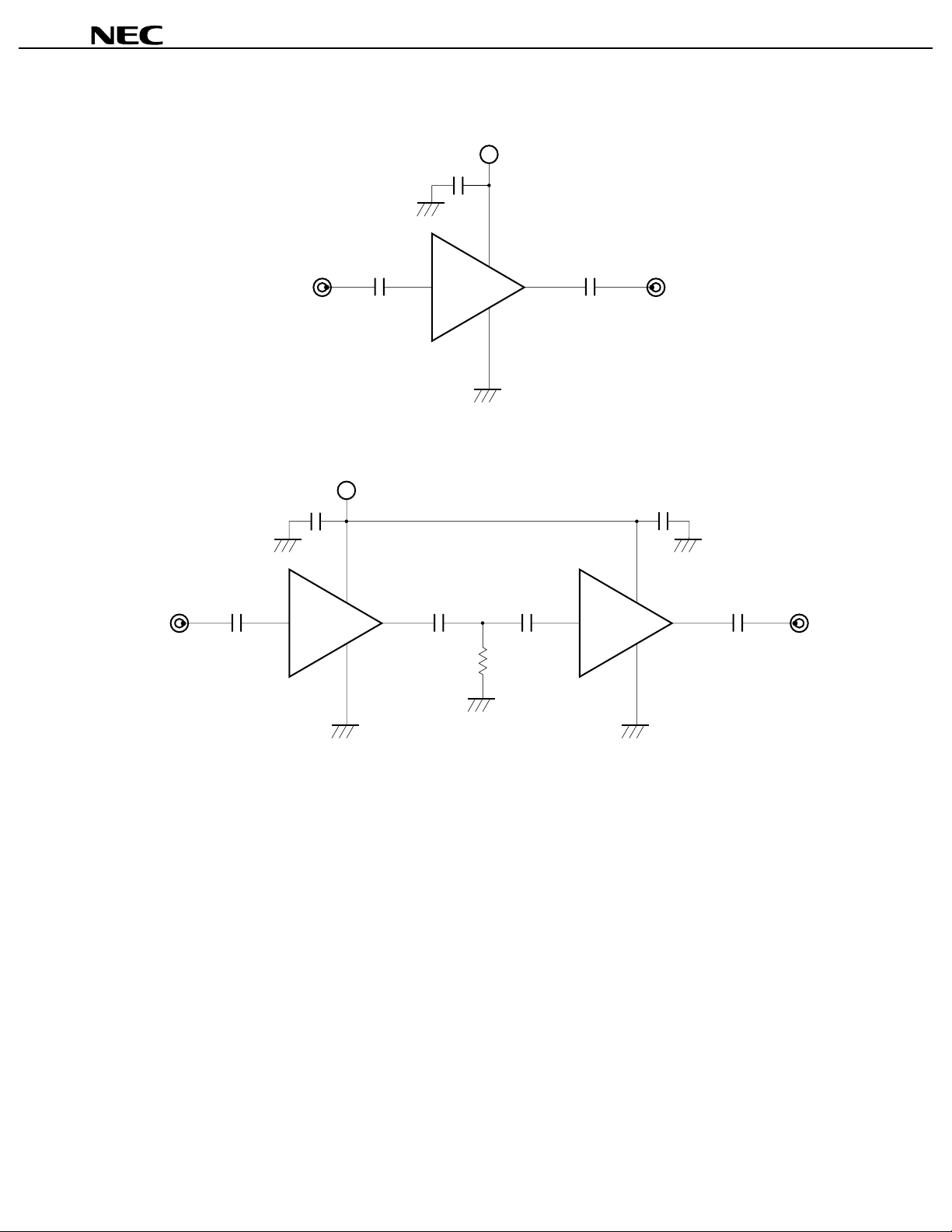
TEST CIRCUIT
50
IN OUT
C1 C2
Ω 50 Ω
1 000 pF 1 000 pF
EXAMPLE OF APPLICATION CIRCUIT
V
CC
1 000 pF
3
C
µµµµ
PC2791TB
CC
V
4
36
1, 2, 5
µµµµ
PC2792TB
1 000 pF
C
3
4
C
50 Ω 50 Ω
IN OUT
1
6
1 000 pF 1 000 pF 1 000 pF
3
1, 2, 5
C
4
C
5
6
R
1
50 to 200 Ω
To stabilize operation,
please connect R
1
, C
1 000 pF
C
6
4
3
1, 2, 5
5
2
C
1 000 pF
The application circuits and their parameters are for reference only and are not intended for use in actual design-ins.
CAPACITORS FOR THE VCC, INPUT AND OUTPUT PINS
1 000 pF capacitors are recommendable as bypass capacitor for VCC pin and coupling capacitors for input/output
pins.
Bypass capacitor for VCC pin is intended to minimize VCC pin’s ground impedance. Therefore, stable bias can be
supplied against VCC fluctuation.
Coupling capacitors for input/output pins are intended to minimize RF serial impedance and cut DC.
To get flat gain from 100 MHz up, 1 000 pF capacitors are assembled on the test circuit. [Actually, 1 000 pF
capacitors give flat gain at least 10 MHz. In the case of under 10 MHz operation, increase the value of coupling
capacitor such as 2 200 pF. Because the coupling capacitors are determined by the equation of C = 1/(2 π fZs).]
Data Sheet P11863EJ2V0DS00
5
Page 6
µµµµ
,
PC2791TB
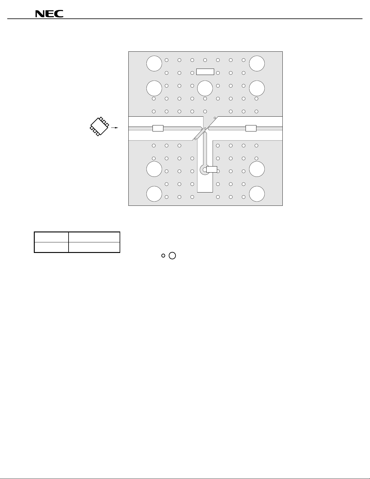
ILLUSTRATION OF THE TEST CIRCUIT ASSEMBLED ON EVALUATION BOARD
AMP-3
Top View
1
2
3
C2S
6
5
4
Mounting direction
(Marking is an example
for PC2791TB)
µ
IN
C
V
CC
C
C
OUT
µµµµ
PC2792TB
COMPONENT LIST
Value
C 1 000 pF
For more information on the use of this IC, refer to the following application note: USAGE AND APPLICATIONS
OF 6-PIN MINI-MOLD, 6-PIN SUPER MINI-MOLD SILICON HIGH-FREQUENCY WIDEBAND AMPLIFIER MMIC
(P11976E).
Notes
1. 30 × 30 × 0.4 mm double sided copper clad polyimide board.
2. Back side : GND pattern
3. Solder plated on pattern
4.
: Through holes
6
Data Sheet P11863EJ2V0DS00
Page 7

µµµµ
,
PC2791TB
µµµµ
PC2792TB
TYPICAL CHARACTERISTICS (Unless otherwise specified, TA = +25
PC2791TB
−−−−
µµµµ
9
8
−−−−
CIRCUIT CURRENT vs. SUPPLY VOLTAGE
30
No Signal
25
20
(mA)
CC
15
10
Circuit Current I
5
0
0123456
Supply Voltage VCC (V) Operating Ambient Temperature TA (°C)
NOISE FIGURE, INSERTION POWER GAIN vs. FREQUENCY
(dB)
P
15
10
G
P
VCC = 5.0 V
VCC = 5.5 V
VCC = 4.5 V
CIRCUIT CURRENT vs. OPERATING AMBIENT TEMPERATURE
30
No Signal
V
CC
= 5.0 V
25
20
(mA)
CC
15
10
Circuit Current I
5
0
−60 −40 −20 0 +20 +40 +60 +80 +100
INSERTION POWER GAIN vs. FREQUENCY
15
VCC = 5.0 V
(dB)
P
10
TA = +85 °C
C)
°°°°
TA = +25 °C
TA = −40 °C
7
6
Noise Figure NF (dB)
5
4
5
NF
Insertion Power Gain G
0
0.1 0.3 1.0 3.0 0.3 1.0 3.0
0
VCC = 5.0 V
−10
−20
−30
Isolation ISL (dB)
−40
−50
0.1 0.3 1.0 3.0
VCC = 5.5 V
VCC = 4.5 V
VCC = 5.0 V
Frequency f (GHz)
ISOLATION vs. FREQUENCY
Frequency f (GHz)
5
Insertion Power Gain G
0
0.1
Frequency f (GHz)
INPUT RETURN LOSS, OUTPUT RETURN LOSS vs. FREQUENCY
0
RL
VCC = 5.0 V
−10
(dB)
(dB)
out
in
−20
−30
Input Return Loss RL
−40
Output Return Loss RL
−50
0.1 0.3 1.0 3.0
RL
Frequency f (GHz)
in
out
Data Sheet P11863EJ2V0DS00
7
Page 8

,
PC2791TB
−−−−
µµµµ
out (dBm)Saturated Output Power PO (sat) (dBm)
+10
+5
0
−5
µµµµ
PC2791TB
−−−−
OUTPUT POWER vs. INPUT POWER OUTPUT POWER vs. INPUT POWER
+10
+5
0
−5
f = 500 MHz
VCC = 5.0 V
TA = +85 °C
TA = +25 °C
f = 500 MHz
VCC = 5.5 V
VCC = 5.0 V
VCC = 4.5 V
µµµµ
PC2792TB
TA = −40 °C
−10
−15
Output Power P
−20
−25
Input Power Pin (dBm) Input Power Pin (dBm)
SATURATED OUTPUT POWER vs. FREQUENCY
+8
+6
+4
+2
0
−2
−4
VCC = 5.5 V
VCC = 4.5 V
f = 500 MHz
VCC = 5.0 V
−10
−15
Output Power Pout (dBm)
−20
−25
−35 −30 −25 −20 −15 −10 −50−35 −30 −25 −20 −15 −10 −50
THIRD ORDER INTERMODULATION DISTORTION
vs. OUTPUT POWER OF EACH TONE
−60
f1 = 500 MHz
3 (dBc)
−50
−40
−30
−20
−10
VCC = 5.0 V
VCC = 4.5 V
f2 = 504 MHz
VCC = 5.5 V
Third Order Intermodulation Distortion IM
−6
0.1 0.3 1.0 3.0 +2−14 −10 −6 −2−12 −8 −40
Frequency f (GHz) Output Power of Each Tone PO (each) (dBm)
8
Data Sheet P11863EJ2V0DS00
0
Page 9

µµµµ
,
PC2791TB
µµµµ
PC2792TB
S-PARAMETER (TA = +25
PC2791TB
−−−−
µµµµ
-FREQUENCY
S
11
−−−−
C, VCC = 5.0 V)
°°°°
1.0 G
0.1 G
3.0 G
2.0 G
S22-FREQUENCY
0.1 G
1.0 G
2.0 G
Data Sheet P11863EJ2V0DS00
9
Page 10

µµµµ
,
PC2791TB
µµµµ
PC2792TB
TYPICAL S-PARAMETER VALUES (TA = +25
PC2791TB
−−−−
µµµµ
VCC = 5.0 V, ICC = 17.0 mA
FREQUENCY S
MHz MAG.ANG.MAG.ANG.MAG.ANG.MAG.ANG.
100.0000 0.155 11.8 4.157 –8.1 0.085 –4.4 0.211 174.9 1.53
200.0000 0.191 21.7 4.179 –16.4 0.081 –7.2 0.203 168.6 1.56
300.0000 0.240 25.3 4.193 –24.6 0.079 –11.0 0.192 163.1 1.56
400.0000 0.290 25.6 4.245 –33.2 0.075 –11.1 0.179 156.8 1.59
500.0000 0.337 22.9 4.288 –42.4 0.068 –13.2 0.161 152.3 1.65
600.0000 0.383 18.1 4.320 –51.7 0.064 –13.3 0.140 149.8 1.69
700.0000 0.418 11.0 4.316 –61.9 0.059 –13.2 0.115 149.8 1.74
800.0000 0.459 3.2 4.316 –72.0 0.054 –11.4 0.087 156.4 1.81
900.0000 0.499 –4.9 4.268 –82.3 0.049 –8.3 0.067 175.9 1.90
1000.0000 0.553 –12.7 4.243 –91.9 0.045 –1.1 0.069 –155.3 1.88
1100.0000 0.604 –19.5 4.218 –102.2 0.045 4.7 0.097 –138.9 1.72
1200.0000 0.647 –26.4 4.140 –113.2 0.041 13.4 0.133 –137.3 1.71
1300.0000 0.670 –33.9 3.981 –124.8 0.045 20.2 0.175 –140.2 1.53
1400.0000 0.672 –42.4 3.753 –136.1 0.049 27.7 0.214 –145.4 1.50
1500.0000 0.665 –50.1 3.473 –146.3 0.054 28.4 0.251 –152.7 1.47
1600.0000 0.659 –57.4 3.169 –155.5 0.058 33.3 0.279 –159.6 1.53
1700.0000 0.653 –65.1 2.924 –164.3 0.063 32.8 0.302 –166.3 1.55
1800.0000 0.645 –71.8 2.680 –172.6 0.067 33.0 0.320 –172.9 1.60
1900.0000 0.642 –77.8 2.490 –179.7 0.071 31.2 0.328 –178.8 1.63
2000.0000 0.621 –83.3 2.302 173.0 0.071 31.0 0.336 175.6 1.84
2100.0000 0.605 –89.3 2.137 166.6 0.072 30.6 0.340 170.4 1.98
2200.0000 0.577 –94.9 1.977 160.2 0.074 30.3 0.344 165.3 2.19
2300.0000 0.561 –101.0 1.838 154.2 0.076 31.4 0.343 161.7 2.35
2400.0000 0.536 –106.7 1.714 148.2 0.075 30.8 0.345 158.1 2.62
2500.0000 0.521 –111.7 1.596 142.9 0.078 31.2 0.343 154.9 2.77
2600.0000 0.509 –116.1 1.499 137.1 0.078 31.4 0.342 151.7 2.98
2700.0000 0.493 –120.9 1.416 132.2 0.080 32.1 0.340 149.4 3.12
2800.0000 0.482 –125.0 1.353 126.6 0.080 34.2 0.336 146.9 3.33
2900.0000 0.467 –128.6 1.283 122.6 0.082 33.8 0.341 144.6 3.45
3000.0000 0.453 –132.3 1.222 116.8 0.085 34.0 0.341 142.5 3.55
3100.0000 0.441 –137.2 1.172 113.1 0.087 34.2 0.341 140.4 3.68
−−−−
11
C)
°°°°
21
S
12
S
22
S
K
10
Data Sheet P11863EJ2V0DS00
Page 11

µµµµ
,
PC2791TB
µµµµ
PC2792TB
TYPICAL CHARACTERISTICS (Unless otherwise specified, TA = +25
PC2792TB
−−−−
µµµµ
7
6
−−−−
CIRCUIT CURRENT vs. SUPPLY VOLTAGE
35
No Signal
30
25
(mA)
CC
20
15
10
Circuit Current I
5
0
0123456
Supply Voltage VCC (V) Operating Ambient Temperature TA (°C)
NOISE FIGURE, INSERTION POWER GAIN vs. FREQUENCY
25
20
(dB)
P
15
G
P
VCC = 4.5 V
VCC = 5.5 V
VCC = 5.0 V
CIRCUIT CURRENT vs. OPERATING AMBIENT TEMPERATURE
35
No Signal
CC
= 5.0 V
V
30
25
(mA)
CC
20
15
10
Circuit Current I
5
0
−60 −40 −20 0 +20 +40 +60 +80 +100
INSERTION POWER GAIN vs. FREQUENCY
25
VCC = 5.0 V
20
(dB)
P
TA = −40 °C
15
C)
°°°°
TA = +25 °C
TA = +85 °C
5
10
Insertion Power Gain G
4
Noise Figure NF (dB)
3
5
NF
0
0.1 0.3 1.0 3.0 0.3 1.0 3.0
0
VCC = 5.0 V
−10
−20
−30
Isolation ISL (dB)
−40
−50
0.1 0.3 1.0 3.0
VCC = 5.5 V
VCC = 5.0 V
VCC = 4.5 V
Frequency f (GHz)
ISOLATION vs. FREQUENCY
Frequency f (GHz)
10
Insertion power Gain G
5
0
0.1
Frequency f (GHz)
INPUT RETURN LOSS, OUTPUT RETURN LOSS vs. FREQUENCY
0
RL
out
−10
(dB)
(dB)
out
in
−20
RL
−30
Input Return Loss RL
−40
Output Return Loss RL
−50
0.1 0.3 1.0 3.0
in
Frequency f (GHz)
VCC = 5.0 V
Data Sheet P11863EJ2V0DS00
11
Page 12

,
PC2792TB
−−−−
µµµµ
+10
+5
(dBm)Saturated Output Power P
out
−5
−10
−−−−
OUTPUT POWER vs. INPUT POWER OUTPUT POWER vs. INPUT POWER
f = 500 MHz
0
VCC = 5.0 V
VCC = 5.5 V
VCC = 4.5 V
+10
+5
(dBm)
out
−5
−10
f = 500 MHz
VCC = 5.0 V
0
µµµµ
PC2791TB
TA = +85 °C
TA = +25 °C
µµµµ
PC2792TB
−15
Output Power P
−20
−25
Input Power Pin (dBm) Input Power Pin (dBm)
SATURATED OUTPUT POWER vs. FREQUENCY
+10
VCC = 5.5 V
+8
(dBm)
+6
O (sat)
+4
+2
VCC = 4.5 V
0
−2
−4
0.1 0.3 1.0 3.0 +4−12 −8 −40−10−16 −14 −6 −2 +2
Frequency f (GHz) Output Power of Each Tone P
f = 500 MHz
VCC = 5.0 V
−15
Output Power P
−20
−25
−40 −35 −30 −25 −20 −15 −10 −5−40 −35 −30 −25 −20 −15 −10 −5
THIRD ORDER INTERMODULATION DISTORTION
−60
(dBc)
3
−50
−40
−30
−20
−10
Third Order Intermodulation Distortion IM
0
TA = −40 °C
vs. OUTPUT POWER OF EACH TONE
VCC = 5.5 V
VCC = 5.0 V
VCC = 4.5 V
f1 = 500 MHz
f2 = 504 MHz
O (each)
(dBm)
12
Data Sheet P11863EJ2V0DS00
Page 13

µµµµ
,
PC2791TB
µµµµ
PC2792TB
S-PARAMETER (TA = +25
PC2792TB
−−−−
µµµµ
-FREQUENCY
S
11
−−−−
C, VCC = 5.0 V)
°°°°
0.1 G
1.0 G
2.0 G
S22-FREQUENCY
0.1 G
1.0 G
2.0 G
Data Sheet P11863EJ2V0DS00
13
Page 14

µµµµ
,
PC2791TB
µµµµ
PC2792TB
TYPICAL S-PARAMETER VALUES (TA = +25
PC2792TB
−−−−
µµµµ
VCC = 5.0 V, ICC = 19.0 mA
FREQUENCY S
MHz MAG.ANG.MAG.ANG.MAG.ANG.MAG.ANG.
100.0000 0.029 –8.4 11.334 –11.1 0.038 0.4 0.205 169.7 1.34
200.0000 0.040 12.5 11.414 –22.4 0.038 1.8 0.194 157.6 1.34
300.0000 0.056 16.9 11.459 –34.1 0.036 2.7 0.180 145.4 1.37
400.0000 0.076 17.9 11.525 –46.2 0.036 3.7 0.160 130.1 1.39
500.0000 0.090 10.7 11.506 –58.9 0.035 5.3 0.137 113.0 1.42
600.0000 0.103 0.3 11.394 –72.0 0.034 8.9 0.110 91.0 1.47
700.0000 0.122 –14.9 11.159 –85.6 0.034 11.6 0.090 56.4 1.48
800.0000 0.148 –28.8 10.840 –99.5 0.034 13.9 0.094 8.9 1.50
900.0000 0.181 –40.4 10.239 –113.7 0.032 19.9 0.127 –26.9 1.58
1000.0000 0.219 –48.0 9.577 –127.1 0.031 22.9 0.174 –51.7 1.68
1100.0000 0.248 –54.0 8.783 –140.5 0.031 27.1 0.222 –71.0 1.71
1200.0000 0.271 –60.3 7.883 –153.0 0.032 32.3 0.264 –86.7 1.76
1300.0000 0.277 –67.2 6.929 –164.4 0.034 39.4 0.299 –101.0 1.87
1400.0000 0.286 –77.3 6.074 –174.3 0.035 44.0 0.322 –112.8 1.99
1500.0000 0.298 –86.0 5.338 177.3 0.038 49.1 0.341 –123.3 2.04
1600.0000 0.311 –93.2 4.709 169.7 0.040 54.9 0.350 –131.9 2.20
1700.0000 0.328 –99.6 4.206 162.6 0.046 56.5 0.358 –139.2 2.11
1800.0000 0.338 –105.2 3.793 156.0 0.048 58.3 0.360 –145.8 2.24
1900.0000 0.347 –110.0 3.474 150.4 0.053 60.5 0.356 –151.1 2.22
2000.0000 0.345 –115.4 3.179 144.6 0.055 60.4 0.355 –156.0 2.33
2100.0000 0.349 –121.1 2.926 138.7 0.059 60.3 0.350 –160.4 2.37
2200.0000 0.353 –126.8 2.704 133.6 0.063 60.5 0.346 –164.6 2.42
2300.0000 0.365 –131.5 2.513 128.2 0.069 61.7 0.339 –166.9 2.37
2400.0000 0.371 –136.3 2.345 122.8 0.072 60.7 0.335 –169.0 2.42
2500.0000 0.377 –139.3 2.192 118.0 0.077 60.6 0.329 –170.9 2.42
2600.0000 0.378 –142.3 2.059 112.6 0.082 61.3 0.324 –172.3 2.44
2700.0000 0.380 –146.4 1.931 108.2 0.083 59.9 0.316 –173.1 2.56
2800.0000 0.382 –150.0 1.827 102.7 0.091 59.9 0.314 –174.0 2.48
2900.0000 0.381 –153.4 1.727 99.0 0.094 59.4 0.317 –174.5 2.52
3000.0000 0.380 –157.0 1.633 93.7 0.098 57.4 0.318 –175.1 2.56
3100.0000 0.390 –160.4 1.557 90.1 0.102 58.2 0.318 –175.2 2.54
−−−−
11
C)
°°°°
21
S
12
S
22
S
K
14
Data Sheet P11863EJ2V0DS00
Page 15

,
PACKAGE DIMENSIONS
6 PIN SUPER MINIMOLD (UNIT: mm)
µµµµ
PC2791TB
µµµµ
PC2792TB
+0.1
0.2 0.15
–0.05
0.1 MIN.
2.1 ±0.1
1.25 ±0.1
0.65 0.65
1.3
2.0 ±0.2
0.7
0.9 ±0.1
+0.1
–0.05
0 to 0.1
Data Sheet P11863EJ2V0DS00
15
Page 16

µµµµ
,
PC2791TB
µµµµ
PC2792TB
NOTES ON CORRECT USE
(1) Observe precautions for handiling because of electro-static sensitive devices.
(2) Form a ground pattern as wide as possible to minimize ground impedance (to prevent undesired oscillation).
All the ground pins must be connected together with wide ground pattern to decrease impedance difference.
(3) The bypass capacitor should be attached to VCC line.
(4) The DC cut capacitor must be each attached to input and output pin.
RECOMMENDED SOLDERING CONDITIONS
This product should be soldered under the following recommended conditions. For soldering methods and
conditions other than those recommended below, contact your NEC sales representative.
Soldering Method Soldering Conditions Recommended Condition Symbol
Infrared Reflow Package peak temperature: 235°C or below
Time: 30 seconds or less (at 210°C)
Count: 3, Exposure limi t: None
VPS Package peak temperature: 215° C or bel ow
Time: 40 seconds or less (at 200°C)
Count: 3, Exposure limi t: None
Partial Heating Pin temperature: 300°C
Time: 3 seconds or less (per side of device)
Exposure limit: None
After opening the dry pack, keep it in a place below 25°C and 65% RH for the allowable storage period.
Note
Caution Do not use different soldering methods together (except for partial heating).
For details of recommended soldering conditions for surface mounting, refer to information document
SEMICONDUCTOR DEVICE MOUNTING TECHNOLOGY MANUAL (C10535E)
Note
Note
Note
.
IR35-00-3
VP15-00-3
–
16
Data Sheet P11863EJ2V0DS00
Page 17

,
[MEMO]
µµµµ
PC2791TB
µµµµ
PC2792TB
Data Sheet P11863EJ2V0DS00
17
Page 18

,
[MEMO]
µµµµ
PC2791TB
µµµµ
PC2792TB
18
Data Sheet P11863EJ2V0DS00
Page 19

,
[MEMO]
µµµµ
PC2791TB
µµµµ
PC2792TB
Data Sheet P11863EJ2V0DS00
19
Page 20

µµµµ
,
PC2791TB
µµµµ
PC2792TB
ATTENTION
OBSERVE PRECAUTIONS
FOR HANDLING
ELECTROSTATIC
SENSITIVE
DEVICES
NESAT (NEC Silicon Advanced Technology) is a trademark of NEC Corporation.
• The information in this document is subject to change without notice. Before using this document, please
confirm that this is the latest version.
• No part of this document may be copied or reproduced in any form or by any means without the prior written
consent of NEC Corporation. NEC Corporation assumes no responsibility for any errors which may appear in
this document.
• NEC Corporation does not assume any liability for infringement of patents, copyrights or other intellectual property
rights of third parties by or arising from use of a device described herein or any other liability arising from use
of such device. No license, either express, implied or otherwise, is granted under any patents, copyrights or other
intellectual property rights of NEC Corporation or others.
• Descriptions of circuits, software, and other related information in this document are provided for illustrative
purposes in semiconductor product operation and application examples. The incorporation of these circuits,
software, and information in the design of the customer's equipment shall be done under the full responsibility
of the customer. NEC Corporation assumes no responsibility for any losses incurred by the customer or third
parties arising from the use of these circuits, software, and information.
• While NEC Corporation has been making continuous effort to enhance the reliability of its semiconductor devices,
the possibility of defects cannot be eliminated entirely. To minimize risks of damage or injury to persons or
property arising from a defect in an NEC semiconductor device, customers must incorporate sufficient safety
measures in its design, such as redundancy, fire-containment, and anti-failure features.
• NEC devices are classified into the following three quality grades:
"Standard", "Special", and "Specific". The Specific quality grade applies only to devices developed based on a
customer designated "quality assurance program" for a specific application. The recommended applications of
a device depend on its quality grade, as indicated below. Customers must check the quality grade of each device
before using it in a particular application.
Standard: Computers, office equipment, communications equipment, test and measurement equipment,
audio and visual equipment, home electronic appliances, machine tools, personal electronic
equipment and industrial robots
Special: Transportation equipment (automobiles, trains, ships, etc.), traffic control systems, anti-disaster
systems, anti-crime systems, safety equipment and medical equipment (not specifically designed
for life support)
Specific: Aircraft, aerospace equipment, submersible repeaters, nuclear reactor control systems, life
support systems or medical equipment for life support, etc.
The quality grade of NEC devices is "Standard" unless otherwise specified in NEC's Data Sheets or Data Books.
If customers intend to use NEC devices for applications other than those specified for Standard quality grade,
they should contact an NEC sales representative in advance.
M7 98. 8
 Loading...