

Page 1
DATA SHEET
DATA SHEET
BIPOLAR ANALOG INTEGRATED CI RCUIT
PC2782GR
µµµµ
L BAND DOWN CONVERTER IC
DESCRIPTION
The µPC2782GR is a Silicon monolithic IC designed for use as L band downconverter. This IC consists of a
Gilbert cell mixer, two stages of LO buffering, local oscillator, external filter port, or a high output IF AGC amplifier and
IF output buffer amplifier.
The package is 20 pins SSOP (shrink small outline package) suitable for high-density surface mount.
FEATURES
• Broad band operation fRF = 0.9 to 2.1 GHz
• 25 dB variable gain IF AGC amplifier
• Low distortion IIP3 = +4.5 dBm (fRF = 2.1 GHz)
• Supply Voltage 5 V
• Packaged in 20 pins SSOP suitable for high-density surface mount
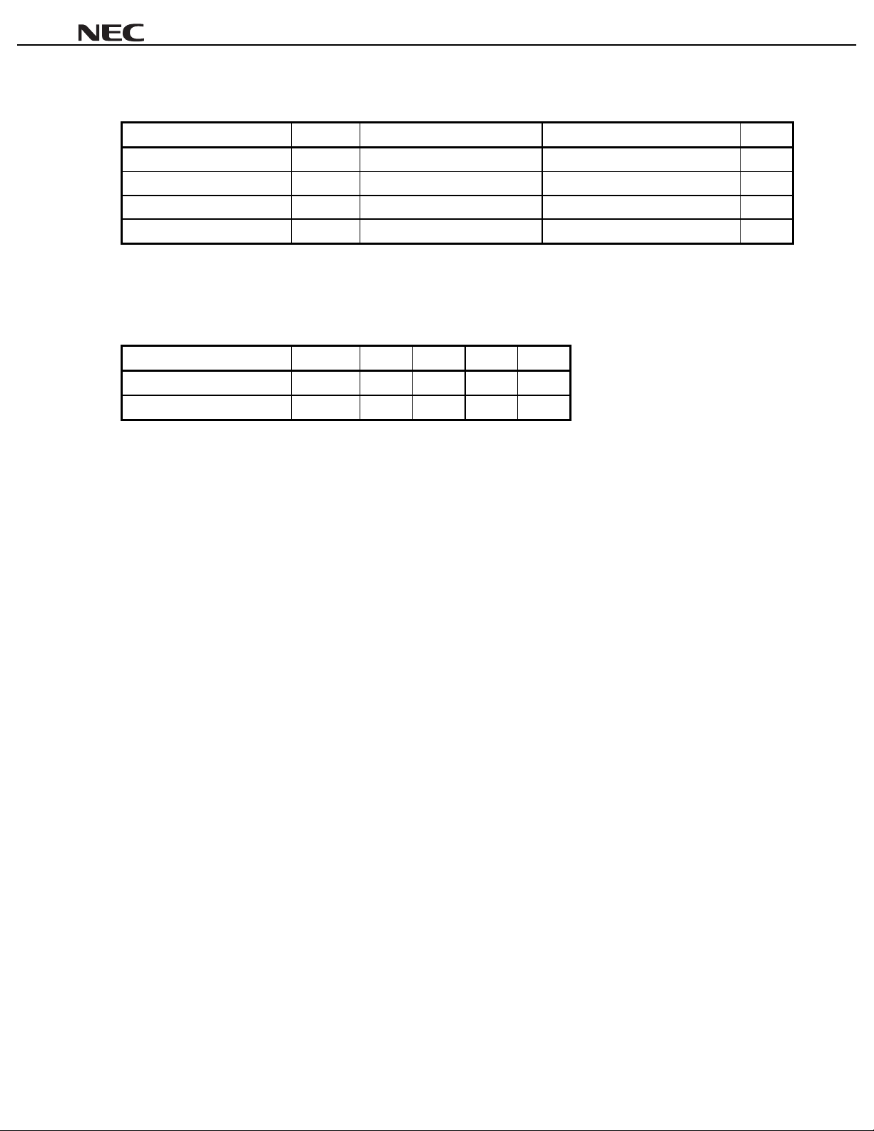
ORDERING INFORMATION
Part Number Package Package Style
µ
PC2782GR-E1 20 pin plastic SSOP (225 m i l ) Embossed tape 12 mm wide. 2. 5 k/REEL.
Pin 1 indicates pull-out di rection of tape
For evaluation sample order, please contact your local NEC sales office. (Part number for sample order:
PC2782GR)
µ
The information in this document is subject to change without notice. Before using this document, please
confirm that this is the latest version.
Not all devices/types available in every country. Please check with local NEC representative for
availability and additional information.
Document No. P11758EJ3V0DS00 (3rd edition)
Date Published October 1999 N CP(K)
Printed in Japan
Caution electro-static sensitive devices.
The mark shows major revised points
©
1996, 1999
Page 2
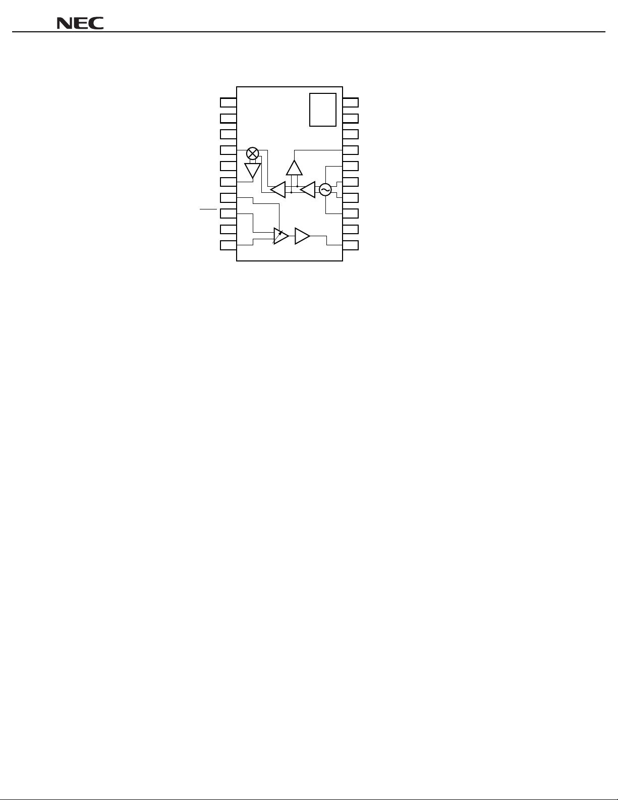
INTERNAL BLOCK DIAGRAM
µµµµ
PC2782GR
V
CC
(IF)
V
CC
(MIX)
GND (MIX)
RF IN
GND (MIX)
IF OUT
V
AGC
IF IN
GND (IF)
IF IN
10
1
2
3
4
5
6
7
8
9
Bias
CKT
V
20
19
V
18
GND (LO)
17
LO OUT
16
LO (B2)
15
LO (C1)
14
LO (C2)
13
LO (B1)
12
GND (LO)
11
IF OUT
CC
(LO)
CC
(LO OUT)
2
Data Sheet P11758EJ3V0DS00
Page 3
µµµµ
PC2782GR
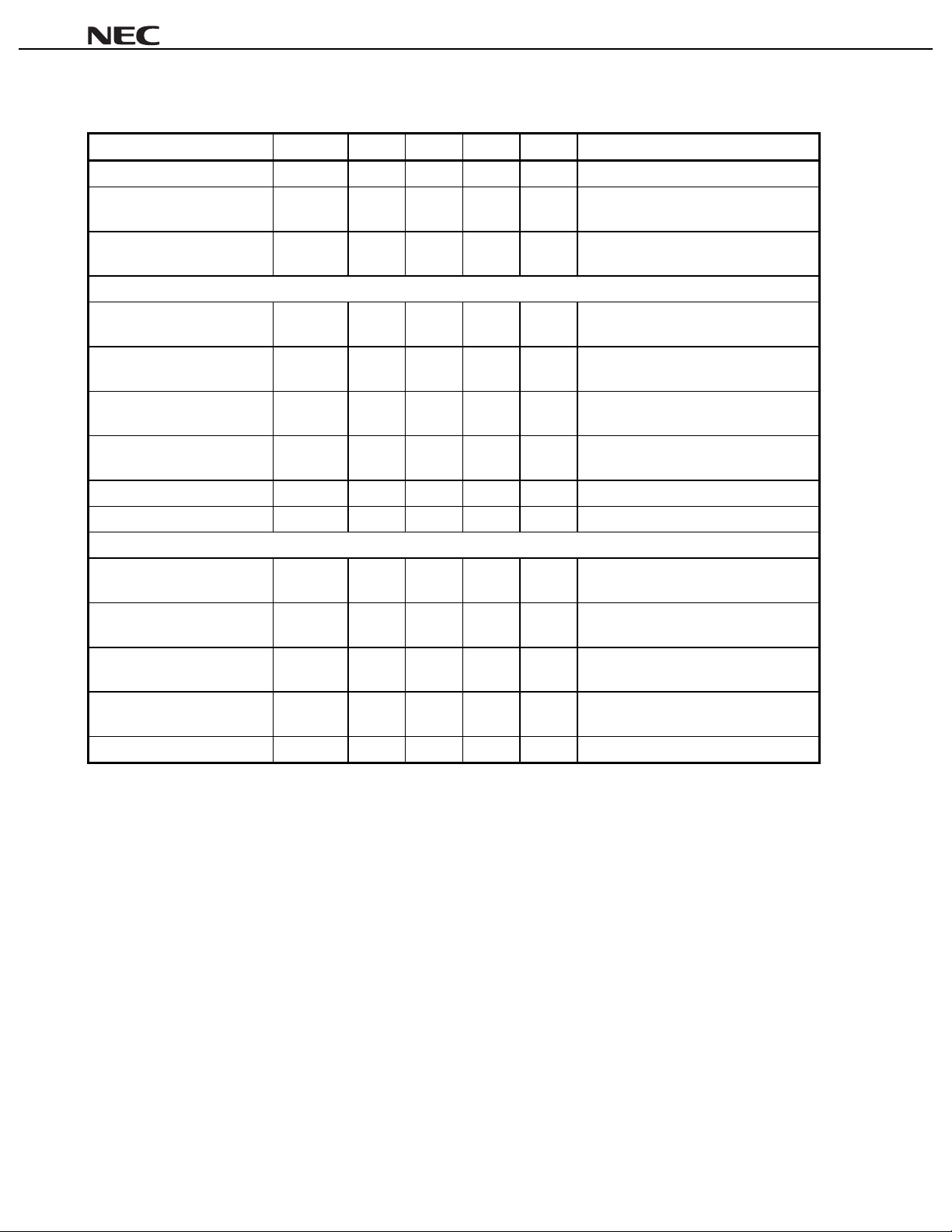
Pin No. Symbol
Pin Volt
TYP.(V)
Functions and Explanation Equivalent Circuit
1VCC (IF) 5.00 Power supply pin of IF AGC A mp.
2VCC (MIX) 5.00 Power supply pin of Mixer
3 GND (MIX) 0.00 Ground pin of Mixer.
4 RF IN 2.00 RF signal input pin.
5 GND (MIX) 0.00 Ground pin of Mixer.
6 IF OUT 1.85 Output pin of Mi xer. This pin is
assigned for the emitter follower
output.
2
OSC
4
Reg
5
3
2
MIX
6
Reg
35
7V
AGC
0 to 5 Gain control pin.
This pin’s bias govern the A G C
output level.
AGC
AGC
= 0 V
= 5 V
Maximum gain at V
Minimum gain at V
8 IF IN 2.36 IF signal input pin of IF A G C A m p.
In case of single input, this pin
should be grounded through 1 000
pF capacitor.
9 GND (IF) 0.00 Ground pin of IF AGC Amp.
10 IF IN 2.36 IF signal input pi n of IF AGC Amp.
1
3 kΩ
7
1
VAGC
8
V
AGC
9
10
Reg
9
Data Sheet P11758EJ3V0DS00
3
Page 4
µµµµ
PC2782GR
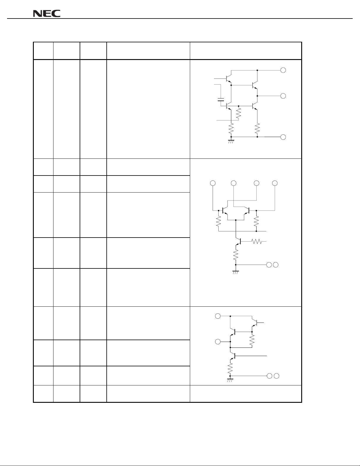
Pin No. Symbol
Pin Volt
TYP.(V)
Functions and Explanation Equivalent Circuit
11 IF OUT 2.55 Out put pi n of IF AGC Amp.
This pin is assigned for em i tter follower push-pull output.
12 GND (LO) 0.00 Ground pin of Oscillator amplifier,
Buffer amplifier, Oscillator output.
13 LO (B1) 2.30 Base pin of oscillator. Connected to
14 pin through capacitor.
14 LO (C2) 5.00 Collector pin of oscillator.
Connected to 15 pin through capacitor. Oscillator frequency bandwidth is depended on this capaci tor.
This pin should be connected to V
through 150 Ω resistor.
15 LO (C1) 5.00 Collector pin of oscillator.
Connected to 14 pin through capacitor. This pin should be c onnected
CC
through 150 Ω resistor.
to V
16 LO (B2) 2.30 Base pin of oscillator. Connected to
15 pin through capacitor.
Assemble LC resonator between 13
pin and 16 pin through 2 pF capacitor to oscillate.
17 LO OUT 3.15 Output pin of Oscillator.
This pin is assigned for em i tter follower output.
1
11
Reg
9
16 15 14 13
CC
19
Reg
Reg
12
18
18 GND (LO) 0.00 Ground pin of Oscillator amplifier,
Buffer amplifier, Oscillator output.
19 VCC (LO) 5.00 Power supply pin of Oscillator output.
20 VCC (LO) 5.00 Power supply pin of Oscillator amp-
lifier, Buffer amplifier.
4
Data Sheet P11758EJ3V0DS00
17
Reg
12 18
Page 5
Absolute Maximum Ratings (TA = 25 °C unless otherwise specified)
Parameter Symbol Test Conditions Rating Unit
µµµµ
PC2782GR
Supply Votage V
Power dissipation P
Operation temperature range T
Storage temperature range T
Mounted on 50 × 50 × 1.6 mm double copper epoxy glass board.
*1
CC
TA = 85 °C
D
A
stg
*1
Recommended Operating Range
Parameter Symbol MIN. TYP. MAX. Unit
Supply Voltage V
Operating temperature range T
CC
A
4.5 5.0 5.5 V
40 +25 +85 °C
−
6.0 V
430 mW
40 to +85 °C
−
55 to +150 °C
−
Data Sheet P11758EJ3V0DS00
5
Page 6
Electrical Characteristics (TA = 25 °C, VCC = 5 V)
Parameter Symbol MIN. TYP. MAX. UNIT Test Conditions
µµµµ
PC2782GR
Circuit Current I
CC
46 66 78 mA
RF Input Frequency Range RF BW 0.9 2.1 GHz PRF = −20 dBm, P
No input signal
OSC
IF
= 480 MHz, −3 dB down
f
= −10 dBm
IF Output Frequency Range IF BW 150 500 MHz fRF = 2.1 GHz, PRF = −20 dBm
OSC
= −10 dBm, −3 dB down
P
Mixer Section
Conversion Gain CG1 7 10 13 dB fRF = 900 MHz, PRF = −30 dBm
OSC
= 1 380 MHz, P
f
OSC
= −10 dBm
Conversion Gain 2 CG2 8 11 14 dB fRF = 2.1 GHz, PRF = −30 dBm
Maximum Output Power 1 P
Maximum Output Power 2 P
O (sat)
O (sat)
Noise Figure 1 NF1
Noise Figure 2 NF2
1+2 +5
2+2 +5
−
−
11.0 14.0 dB
13.5 16.5 dB
−
−
OSC
= 2.58 GHz, P
f
dBm fRF = 900 MHz, PRF = 0 dBm
OSC
= 1 380 MHz, P
f
dBm fRF = 2.1 GHz, PRF = 0 dBm
OSC
= 2.58 GHz, P
f
RF
f
= 900 MHz, P
RF
f
= 2.1 GHz, P
OSC
= −10 dBm
OSC
OSC
= −10 dBm
OSC
= −10 dBm
OSC
= −10 dBm
= −10 dBm
IF Amp. Section
AGC
AGC
= 0 V
= 0 V
IF Input Frequency Range IFinBW 150
O (sat)
∆
IF
AGC
G
20 23 26 dB fIF = 480 MHz, PIF = −30 dBm
3+5 +8
20 25
−
IF Power Gain G
Maximum Output Power 3 P
AGC Dynamic range
Noise Figure 3 NF3
−
500 MHz PIF = −30 dBm, V
−
−
dBm fIF = 480 MHz, PIF = 0 dBm
dB fIF = 480 MHz, PIF = −30 dBm
12.0 15.0 dB
3 dB down
−
AGC
= 0
V
AGC
= 0 V
V
AGC
= 0 to 5 V
V
IF
f
= 480 MHz, V
*2
*2
*2
*2
*2
*2
*2
*3
*3
*4
*4
*4
*4
*5
by measurement circuit 1
*2
by measurement circuit 2
*3
by measurement circuit 4
*4
by measurement circuit 5
*5
6
Data Sheet P11758EJ3V0DS00
Page 7

µµµµ
PC2782GR
Standard Characteristics (TA = 25
Symbol
Mixer Section
Input Intercept Point 1 IIP31
Input Intercept Point 2 IIP32
Third Intermodulation
Distortion 1
Third Intermodulation
Distortion 2
Oscillator Output Power P
Oscillator Frequency Range f
IF Amp. Section
Output Intercept Point OIP
by measurement circuit 3
*6
by application circuit example
*7
by measurement circuit 6
*8
IM31
IM32
C, VCC = 5 V)
°°°°
OSC
OSC
3
Reference Value
MIN. TYP. MAX.
−
−
−
−
0
+4.5
50
59
−
−
−
−
−−15−
1.3
−
+15.5
−
2.6 GHz
−
UNIT Test ConditionsParameter
dBm fRF = 900, 930 MHz, f
OSC
= −10 dBm
P
dBm fRF = 2.1, 2.13 GHz, f
OSC
= −10 dBm
P
OSC
= 1 380 MHz
OSC
= 2.58 GHz
dBc fRF = 900, 930 MHz, PRF = −25 dBm each
OSC
= 1 380 MHz, P
f
OSC
= −10 dBm
dBc fRF = 2.1, 1.13 GHz, PRF = −25 dBm each
OSC
= 2.58 GHz, P
f
OSC
= −10 dBm
dBm
IF
= 480, 510 MHz
dBm
f
*6
*6
*6
*6
*7
*7
*8
Data Sheet P11758EJ3V0DS00
7
Page 8

µµµµ
PC2782GR
Typical Characteristics (VCC = 5 V, TA = 25
fRF vs. CG (MIXER)
12
10
8
6
4
CG - Conversion Gain - dB
2
0
800
1 000 1 400 1 800 2 200
f
RF
- Input Frequency - MHz
Pin vs. P
10
0
out
(MIXER)
f
IF
= 480 MHz
P
OSC
= –10 dBm
C)
°°°°
IF
vs. CG (MIXER)
f
14
12
10
8
6
4
CG - Conversion Gain - dB
2
fRF = 2.1 GHz
RF
= –20 dBm
P
0 200 400 600 800
f
IF
- Intermediate Frequency - MHz
in
vs. P
out
P
(MIXER)
10
0
–10
–20
- Output Power - dBm
out
P
–30
–40
–40
–30 –20 –10 0 10
P
20
IF
= 480 MHz
f
OSC
= –10 dBm
P
18
16
14
12
NF - Noise Figure - dB
10
8
0.8 1 1.2 1.4 1.6 1.8 2 2.2
0.6
f
RF
- Input Frequency - GHz
fRF = 900 MHz
OSC
f
OSC
P
in
- Input Power - dBm
f
RF
vs. NF (MIXER)
= 1 380 MHz
= –10 dBm
–10
–20
- Output Power - dBm
out
P
–30
–40
–40
–30 –20 –10 0 10
in
P
70
60
50
40
30
- Circuit Current - mA
20
CC
I
10
0
123456
V
CC
fRF = 2.1 GHz
OSC
f
OSC
P
- Input Power - dBm
CC
vs. I
CC
V
VCC: 6 → 0 V
No input signal
- Supply Voltage - V
= 2.58 GHz
= –10 dBm
8
Data Sheet P11758EJ3V0DS00
Page 9

µµµµ
PC2782GR
Pin vs. Pout (IFAGCAmp)
10
0
–10
–20
- Output Power - dBm
out
P
–30
–40
–40
–30 –20 –10 0 10
in
P
f
20
15
IF
f
V
- Input Power - dBm
IF
vs. NF (IFAGCAmp)
= 480 MHz
AGC
= 0 V
30
25
20
Gain (dB)
15
10
30
25
20
IF
vs. CG (IFAGCAmp)
f
P
IF
= –30 dBm
AGC
= 0 V
V
0
200 400 600
IF
- Intermediate Frequency - MHz
f
AGCVoltage vs. Gain
IF
= 480 MHz
f
IF
= –30 dBm
P
10
NF - Noise Figure - dB
5
200
0
f
IF
- Intermediate Frequency - MHz
V
AGC
= 0 V
400 600 800 1 000
15
10
IF Amp Gain (dB)
5
0
–5
0
123456
V
AGC
- AGC Voltage - V
Data Sheet P11758EJ3V0DS00
9
Page 10

µµµµ
PC2782GR
Standard Characteristics (VCC = 5 V, TA = 25
IM3 (MIXER)
10
–10
–30
–50
- Output Power - dBm
out
P
–70
–90
10
–40
–30 –20 –10 0 10
in
- Input Power - dBm
P
IM3 (IFAGCAmp)
RF
= 900, 930 MHz
f
f
OSC
= 1 380 MHz
OSC
= –10 dBm
P
C)
°°°°
3
(MIXER)
IM
10
–10
–30
–50
- Output Power - dBm
out
P
–70
–90
–40
ATTEN 10 dB
0 dBm 10 dB/
RL
0
–30 –20 –10 0 10
in
- Input Power - dBm
P
Oscillator Frequency Range
1.268 G
RF
= 2.1, 2.13 GHz
f
f
OSC
= 2.58 GHz
OSC
= –10 dBm
P
2.618 G
–10
–30
–50
- Output Power - dBm
out
P
–70
–90
–40
–30 –20 –10 0 10
P
IF
= 480, 510 MHz
f
AGC
= 0 V
V
in
- Input Power - dBm
–50
- Oscillator Output Power - dBm
OSC
P
CENTER 2.000 GHz SPAN 1.800 GHz
RBW 1.0 MHz VBW 1.0 MHz SWP 50 ms
10
Data Sheet P11758EJ3V0DS00
Page 11

µµµµ
PC2782GR
Standard Characteristics (VCC = 5 V, TA =
fRF vs. CG (MIXER)
600
TA = –40 ˚C
TA = 85 ˚C
fIF = 480 MHz
OSC
= –10 dBm
P
1 000 1 400 1 800 2 200
f
RF
- Input Frequency - MHz
Pin vs. P
out
(MIXER)
TA = –40 ˚C
TA = 85 ˚C
12
10
8
6
4
CG - Conversion Gain - dB
2
0
10
0
–10
40
C, 85
−−−−
°°°°
C)
°°°°
IF
vs. CG (MIXER)
f
14
TA = –40 ˚C
12
10
TA = 85 ˚C
8
6
4
CG - Conversion Gain - dB
2
0
0
200 400 600 800
IF
- Intermediate Frequency - MHz
f
P
in
vs. P
out
(MIXER)
RF
= 2.1 GHz
f
RF
= –20 dBm
P
10
TA = –40 ˚C
0
TA = 85 ˚C
–10
–20
- Output Power - dBm
out
P
–30
–40
–40
–30 –20 –10 0 10
in
P
20
18
16
14
TA = –40 ˚C
12
NF - Noise Figure - dB
10
8
0.6
0.8 1 1.2 1.4 1.6 1.8 2
RF
- Input Frequency - GHz
f
RF
= 900 MHz
f
OSC
= 1 380 MHz
f
P
OSC
- Input Power - dBm
fRF vs. NF (MIXER)
TA = 85 ˚C
IF
= 480 MHz
f
OSC
= –10 dBm
P
= –10 dBm
–20
- Output Power - dBm
out
P
–30
–40
–40
–30 –20 –10 0 10
in
P
70
60
TA = 85 ˚C
50
40
30
- Circuit Current - mA
20
CC
I
10
12 3 45
0
CC
V
RF
= 2.1 GHz
f
f
OSC
= 2.58 GHz
OSC
P
- Input Power - dBm
V
CC
vs. I
CC
TA = –40 ˚C
No input signal
CC
: 6 → 0 V
V
- Supply Voltage - V
= –10 dBm
6
Data Sheet P11758EJ3V0DS00
11
Page 12

µµµµ
PC2782GR
10
–10
–30
–50
- Output Power - dBm
out
P
–70
–90
–40
–30 –20 –10 0 10
P
10
–10
TA = 85 ˚C
–30
IM3 (MIXER)
TA = 85 ˚C
fRF = 900, 930 MHz
OSC
f
OSC
P
in
- Input Power - dBm
IM3 (IFAGCAmp)
TA = –40 ˚C
= 1 380 MHz
= –10 dBm
10
–10
–30
–50
- Output Power - dBm
out
P
–70
–90
–40
–30 –20 –10 0 10
P
P
10
TA = 85 ˚C
0
–10
IM
3
(MIXER)
f
RF
= 2.1, 2.13 GHz
f
OSC
= 2.58 GHz
OSC
P
in
- Input Power - dBm
in
vs. P
out
(IFAGCAmp)
TA = –40 ˚C
TA = –40 ˚C
TA = 85 ˚C
= –10 dBm
–50
- Output Power - dBm
out
P
–70
TA = –40 ˚C
–90
–40
–30 –20 –10 0 10
P
f
30
25
TA = –40 ˚C
20
Gain - dB
15
10
0
200 400 600
f
IF
- Intermediate Frequency - MHz
IF
f
AGC
V
in
- Input Power - dBm
IF
vs. CG (IFAGCAmp)
TA = 85 ˚C
V
P
= 480,510 MHz
= 0 V
AGC
= 0 V
IF
= –30 dBm
–20
- Output Power - dBm
out
P
–30
–40
–40
–30 –20 –10 0 10
P
25
20
15
10
TA = 85 ˚C
5
IF Amp Gain - dB
0
–5
–10
0
12345
V
f
V
in
- Input Power - dBm
AGCVoltage vs. Gain
TA = –40 ˚C
AGC
- AGC Voltage - V
IF
= 480 MHz
AGC
= 0 V
f
IF
= 480 MHz
P
IF
= –30 dBm
6
12
Data Sheet P11758EJ3V0DS00
Page 13

Measurement Circuit 1
OSC
OUT
µµµµ
PC2782GR
V
CC
Measurement Circuit 2
150 Ω
1 000
pF
1 000
pF
1 000
1 000
pF
pF
150 Ω
20 19 18 17 16 15 14 13 12 11
Bias CKT
12345678910
1 000 pF
RF IN IF OUT
1 000 pF
SG1
(50 Ω)
NF
METER
OSC
OUT
150 Ω
1 000
pF
1 000
pF
1 000
1 000
pF
pF
150 Ω
20 19 18 17 16 15 14 13 12 11
Bias CKT
12345678910
1 000 pF
Noise Source
1 000 pF
V
CC
SG1
(50 Ω)
Data Sheet P11758EJ3V0DS00
13
Page 14

Measurement Circuit 3
OSC
OUT
µµµµ
PC2782GR
V
CC
1 000
1 000
pF
pF
150 Ω
20 19 18 17 16 15 14 13 12 11
Bias CKT
12345678910
1 000 pF
Spectrum
Analyzer
(50 Ω)
SG1
(50 Ω)
SG2
(50 Ω)
1 000 pF
150 Ω
1 000
pF
1 000
pF
SG3
(50 Ω)
Measurement Circuit 4
Spectrum
Analyzer
(50 Ω)
20 19 18 17 16 15 14 13 12 11
Bias CKT
12345678910
1 000
pF
VCC
1 000
pF
VAGC
1 000
pF
SG1
(50 Ω)
1 000 pF
1 000 pF
14
Data Sheet P11758EJ3V0DS00
Page 15

Measurement Circuit 5
Spectrum
Analyzer
(50 Ω)
20 19 18 17 16 15 14 13 12 11
Bias CKT
12345678910
1 000
pF
1 000 pF
µµµµ
PC2782GR
Measurement Circuit 6
VAGC
1 000
pF
1 000
pF
1 000
pF
VCC
20 19 18 17 16 15 14 13 12 11
Bias CKT
12345678910
1 000 pF
1 000 pF
SG1
(50
SG2
(50 Ω)
NF
METER
Noise
Source
Ω)
VCC
1 000
pF
1 000
pF
VAGC
Data Sheet P11758EJ3V0DS00
1 000 pF
15
Page 16

Application Circuit Example
20 19 18 17 16 15 14 13 12 11
Bias CKT
1 000
pF
OSC
OUT
12
k
2 pF
V
T
12 kΩ
150Ω150
to 15 nH
Ω
µµµµ
PC2782GR
4 pF
VCC
* Cv: HVU316
1 000
pF
IF OUT
CVCV
12
k
3 pF1.5 pF3 pF
2 pF
12345678910
1 000
VAGC
pF
1 000
pF
1 000 pF
IF IN
1 000 pF
RF IN IF
OUT
1 000
pF
The application circuits and their parameters are for reference only and are not intended for use in actual design-ins.
16
Data Sheet P11758EJ3V0DS00
Page 17

Illustration of The Application Circuit Assembled on Evaluation Board
V
CC
V
TU
LO OUT LO IN
µµµµ
PC2782GR
RF IN
C1
C2
C13
C11
R5
R3
C12
R2 R1
C10 C6
C9 C7
C8
C14
C3
R4
L
C
V
10
upc2782
AGC OUT
50.0000
C5
AGC INIF OUT
C4
AGC
V
50.0000
C1 to C5 : 1 000 pF
C6, C10 : 2 pF
C7, C9 : 3 pF
C8 : 1.5 pF
C11 to C14 : 1 000 pF
R1 to R3 : 12 kΩ
R4, R5 : 150 Ω
V
: HVU316
C
L : to 15 nH
Data Sheet P11758EJ3V0DS00
φ
pattern should be removed on this application*
: 0.5 mm
7 to 8 mm
17
Page 18

PACKAGE DIMENSIONS
20 PIN PLASTIC SSOP (225 mil) (UNIT: mm)
µµµµ
PC2782GR
20
110
6.7 ± 0.3
1.8 MAX.
1.5 ± 0.1
11
detail of lead end
3˚
6.4 ± 0.2
4.4 ± 0.1
+7˚
–3˚
1.0 ± 0.2
0.5 ± 0.2
0.15
+0.10
–0.05
0.10
0.15
M
0.575 MAX.
0.65
+0.10
0.22
–0.05
0.1 ± 0.1
Each lead centerline is located within 0.10 mm of its true position (T.P.) at maximum material condition.
NOTE
18
Data Sheet P11758EJ3V0DS00
Page 19

µµµµ
PC2782GR
Recommended Soldering Conditions
The following conditions (see table below) must be met when soldering this product.
Please consult with our sales officers in case other soldering process is used or in case soldering is done under
different conditions.
For details of recommended soldering conditions for surface mounting, refer to information document SEMI
CONDUCTOR DEVICE MOUNTING TECHNOLOGY MANUAL (C10535E).
PC2782GR
µµµµ
Soldering process Soldering conditions Symbol
Infrared ray reflow Peak package’s surface temperature: 235 °C or below,
Reflow time: 30 seconds or bel ow (210 °C or higher),
Number of reflow process: 3, Exposure limit
VPS Peak package’s surface temperature: 215 °C or below,
Reflow time: 40 seconds or bel ow (200 °C or higher),
Number of reflow process: 3, Exposure limit
Wave soldering Solder temperature: 260 °C or below,
Reflow time: 10 seconds or bel ow,
Number of reflow process: 1, Exposure limit
Partial heating method Terminal temperature: 300 °C or below,
Flow time: 3 seconds or below,
Exposure limit
Exposure limit before soldering after dry-pack package is opened.
Note
Note
: None
Note
Note
: None
Note
: None
: None
Storage conditions: 25 °C and relative humidity at 65 % or less.
Caution Do not apply more than single process at once, except for “Partial heating method”.
IR35-00-3
VP15-00-3
WS60-00-1
Data Sheet P11758EJ3V0DS00
19
Page 20

µµµµ
PC2782GR
NESAT (NEC Silicon Advanced Technology) is a trademark of NEC Corporation.
• The information in this document is subject to change without notice. Before using this document, please
confirm that this is the latest version.
• No part of this document may be copied or reproduced in any form or by any means without the prior written
consent of NEC Corporation. NEC Corporation assumes no responsibility for any errors which may appear in
this document.
• NEC Corporation does not assume any liability for infringement of patents, copyrights or other intellectual property
rights of third parties by or arising from use of a device described herein or any other liability arising from use
of such device. No license, either express, implied or otherwise, is granted under any patents, copyrights or other
intellectual property rights of NEC Corporation or others.
• Descriptions of circuits, software, and other related information in this document are provided for illustrative
purposes in semiconductor product operation and application examples. The incorporation of these circuits,
software, and information in the design of the customer's equipment shall be done under the full responsibility
of the customer. NEC Corporation assumes no responsibility for any losses incurred by the customer or third
parties arising from the use of these circuits, software, and information.
• While NEC Corporation has been making continuous effort to enhance the reliability of its semiconductor devices,
the possibility of defects cannot be eliminated entirely. To minimize risks of damage or injury to persons or
property arising from a defect in an NEC semiconductor device, customers must incorporate sufficient safety
measures in its design, such as redundancy, fire-containment, and anti-failure features.
• NEC devices are classified into the following three quality grades:
"Standard", "Special", and "Specific". The Specific quality grade applies only to devices developed based on a
customer designated "quality assurance program" for a specific application. The recommended applications of
a device depend on its quality grade, as indicated below. Customers must check the quality grade of each device
before using it in a particular application.
Standard: Computers, office equipment, communications equipment, test and measurement equipment,
audio and visual equipment, home electronic appliances, machine tools, personal electronic
equipment and industrial robots
Special: Transportation equipment (automobiles, trains, ships, etc.), traffic control systems, anti-disaster
systems, anti-crime systems, safety equipment and medical equipment (not specifically designed
for life support)
Specific: Aircraft, aerospace equipment, submersible repeaters, nuclear reactor control systems, life
support systems or medical equipment for life support, etc.
The quality grade of NEC devices is "Standard" unless otherwise specified in NEC's Data Sheets or Data Books.
If customers intend to use NEC devices for applications other than those specified for Standard quality grade,
they should contact an NEC sales representative in advance.
M7 98. 8
 Loading...