

Page 1
DATA SHEET
BIPOLAR ANALOG INTEGRATED CIRCUIT
µ
PC2766GR/GS
WIDE BAND IQ DEMODULATOR FOR DIGITAL VIDEO/DATA RECEIVER
DESCRIPTION
The µPC2766GR/GS is a Silicon monolithic IC designed for use as IQ demodulator in wide dynamic range
compressed video or spread spectrum receivers. This IC consists of a wide band RF amplifier, gain control amplifier,
dual balanced mixers (DBM), Lo buffers, and I & Q output buffer amplifiers.
µ
The package is 20 pin SSOP (shrink small outline package:
for high-density surface mount.
FEATURES
• Broadband operation RF & LO up to 1 000 MHz
IF (IQ) up to 200 MHz
• Wideband IQ phase and amplitude balance Amplitude balance ±0.3 dB (TYP.)
Phase balance ±0.3 degree (TYP.)
• AGC dynamic range 45 dB
• Low distortion; IM
• Supply Voltage 5 V
• Packaged in 20 pin SSOP or 20 pin SOP suitable for high-density surface mount
3 30 dBc
PC2766GR) or 20 pin SOP (µPC2766GS) suitable
ORDERING INFORMATION
PART NUMBER PACKAGE PACKAGE STYLE
µ
PC2766GR-E1
µ
PC2766GS-E1
The information in this document is subject to change without notice. Before using this document, please
confirm that this is the latest version.
Not all devices/types available in every country. Please check with local NEC representative for availability
and additional information.
20 pin plastic SSOP (225 mil)
20 pin plastic SOP (300 mil)
Caution electro-static sensitive device
Embossed tape 12 mm wide. 2.5 k/REEL
Pin 1 indicates pull-out direction of tape
Embossed tape 24 mm wide. 2.5 k/REEL
Pin 1 indicates pull-out direction of tape
Document No. P10193EJ4V0DS00 (4th edition)
Date Published October 1999 N CP(K)
Printed in Japan
The mark shows major revised points.
©
1995, 1999
Page 2
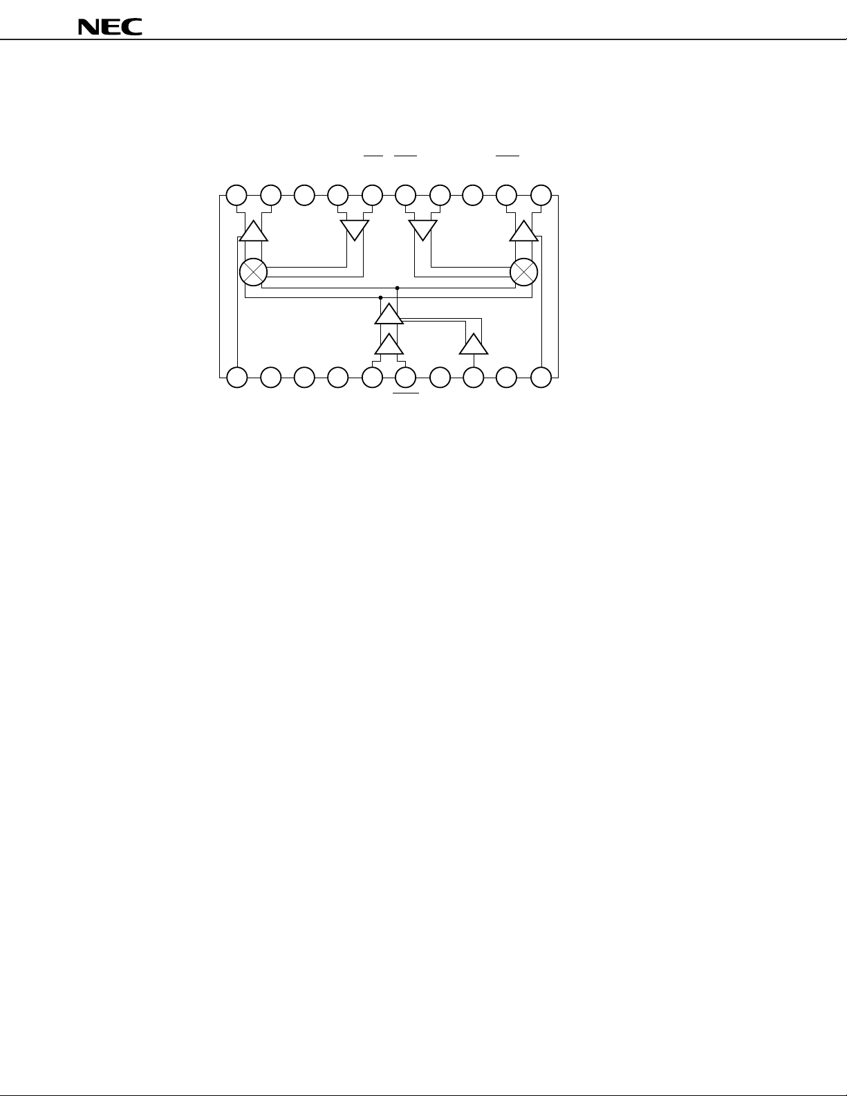
INTERNAL BLOCK DIAGRAM
µ
PC2766GR/GS
I out I out GND
20 19 18 17 16 15 14 13 12 11
I-IF Amp.
I-Lo.Buff.Amp I-Lo.Buff.Amp
I-MIX.
23
1
I trim Vcc
IF. I
Lo I Lo I Lo Q Lo Q GND
IF. I
RF AGC
RF Pre.Amp AGC cont.
4
VccRFGNDRFRF in RF in GNDRFVagc Vcc
678910
5
Q out Q out
IF. Q
I-IF Amp.
Q-MIX.
IF. Q
Q trim
2
Data Sheet P10193EJ4V0DS00
Page 3
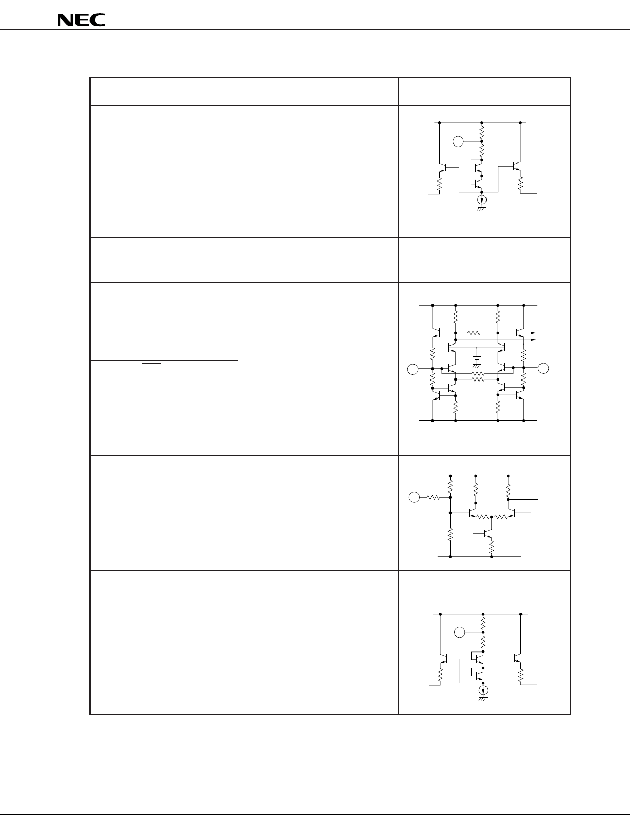
PIN FUNCTIONS
5
6
To next
block
V
CC
10
µ
PC2766GR/GS
PIN No. PIN NAME
1 I Trim 4.2 Trimming pin for I-IF output.
2VCCIF I 5.0 Power supply pin for I-MIXER.
3VCCRF 5.0 Power supply pin for RF and AGC
4 GND RF 0.0 Ground pin of RF and AGC block.
5 RFin 2.6 RF input pin. In case of single input,
6 RFin 2.6
PIN VOLTAGE
TYP. (V)
FUNCTION AND EXPLANATION EQUIVALENT CIRCUIT
block.
6 pin should be grounded through
capacitor.
V
CC
1
7 GND RF 0.0 Ground pin of RF and AGC block.
8VAGC 0 to 5 Gain control pin.
CC
• VAGC = 0 V: Full gain
• VAGC = 5 V: Maximum reduction
9VCCIF Q 5.0 Power supply pin for Q-MIXER.
10 Q Trim 4.2 Trimming pin for Q-IF output.
8
V
Data Sheet P10193EJ4V0DS00
3
Page 4
µ
PC2766GR/GS
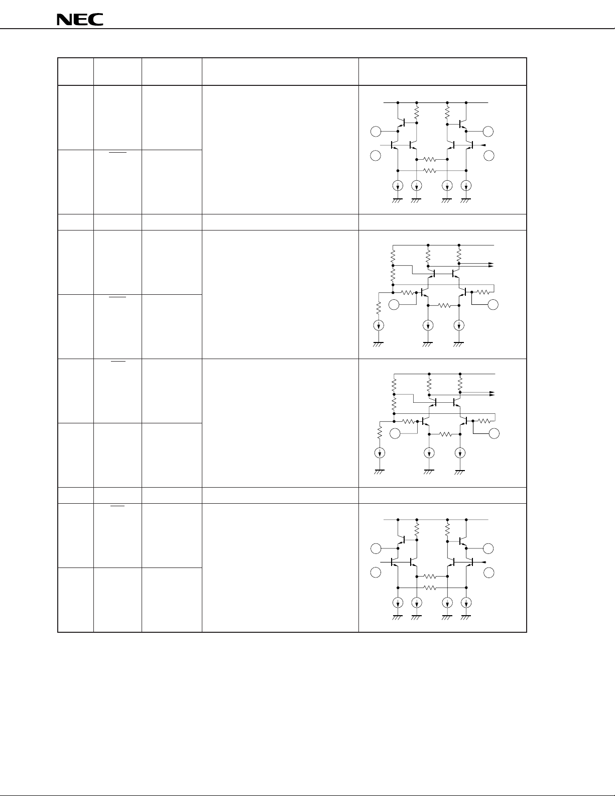
PIN No. PIN NAME
11 Qout 3.3 Q-IF output pin. 11 pin and 12 pin
12 Qout 3.3
13 GNDIF Q 0.0 Ground pin of Q-IF block.
14 Lo Q 2.2 Oscillator signal input pin of
15 Lo Q 2.2
PIN VOLTAGE
TYP. (V)
FUNCTION AND EXPLANATION EQUIVALENT CIRCUIT
are balance outputs.
Q-MIXER. In case of single input,
15 pin should be grounded through
capacitor.
12
V
CC
11
From
before
block
+
_
CC
V
1514
16 Lo I 2.2 Oscillator signal input pin of
I-MIXER. In case of single input,
16 pin should be grounded through
capacitor.
17 Lo I 2.2
18 GNDIF I 0.0 Ground pin of I-IF block.
19 Iout 3.3 I-IF output pin. 19 pin and 20 pin
are balance outputs.
20 Iout 3.3
19
CC
V
20
_
16
V
CC
From
before
block
17
+
4
Data Sheet P10193EJ4V0DS00
Page 5
ABSOLUTE MAXIMUM RATINGS (TA = 25 °C)
µ
PC2766GR
PARAMETER SYMBOL RATING UNIT TEST CONDITIONS
Supply voltage VCC 6.0 V
Power dissipation PD 430 mW TA = 85 °C
Operating temperature range TA –40 to +85 °C
Storage temperature range Tstg –55 to +150 °C
µ
PC2766GS
PARAMETER SYMBOL RATING UNIT TEST CONDITIONS
Supply voltage VCC 6.0 V
Power dissipation PD 650 mW TA = 85 °C
Operating temperature range TA –40 to +85 °C
Storage temperature range Tstg –55 to +150 °C
µ
PC2766GR/GS
Note 1
Note 1
Note 1 Mounted on 50 × 50 × 1.6 mm double epoxy glass board.
RECOMMENDED OPERATING RANGE
µ
PC2766GR/GS
PARAMETER SYMBOL MAX. TYP. MIN. UNIT
Supply voltage VCC 4.5 5.0 5.5 V
Operating temperature range TA –40 +25 +85 °C
Data Sheet P10193EJ4V0DS00
5
Page 6

µ
PC2766GR/GS
ELECTRICAL CHARACTERISTICS (VCC = 5 V, TA = 25 °C,ZL = 250 Ω)
µ
PC2766GR/GS
PARAMETER SYMBOL MIN. TYP. MAX. UNIT TEST CONDITIONS
Supply current ICC – 60 78 mA no input signal
RF input bandwidth RF BW DC - DC - – MHz fIF = 40 MHz, fRF > fLO
IF output bandwidth IF BW DC 200 – MHz fRF = 480 MHz, PLO = –10 dBm
Gain control range GGC 40 45 – dB fRF = 480 MHz, fIF = 40 MHz
IQ phase balance
IQ amplitude balance
Output voltage VO 1.2 1.5 – V P-P fRF = 480 MHz, fIF = 40 MHz
∆φ
∆
G–±0.3 ±0.5 dB fRF = 480 MHz, fIF = 40 MHz
750 1000 IQ phase balance ≤ ±1.5°
fRF > fLO, –3 dB down, Vagc = 0 V
PRF = –30 dBm,
Vagc = 0 – 5 V
– ±0.3 ±1.5 deg fRF = 480 MHz, fIF = 40 MHz
PRF = –30 dBm, PLO = –10 dBm
PRF = –30 dBm, PLO = –10 dBm
Vagc = 0 V
PLO = –10 dBm, ZL = 250 Ω
PLO = –10 dBm
Conversion gain CG 15 20 25 dB fRF = 480 MHz, fIF = 40 MHz
Vagc = 0 V
STANDARD CHARACTERISTICS (REFERENCE VALUES) (VCC = 5 V, TA = 25 °C,ZL = 250 Ω)
µ
PC2766GR/GS
PARAMETER SYMBOL MIN. TYP. MAX. UNIT TEST CONDITIONS
Noise figure NF – 21 – dB fRF = 480 MHz, fIF = 40 MHz
PLO = –10 dBm, Vagc = 0 V
LO to RF isolation LO-RFisol –55–dBfLO = 440 MHz, PLO = –10 dBm
Vagc = 0 V
LO to IF isolation LO-IFisol –10–dBfLO = 440 MHz, PLO = –10 dBm
Vagc = 0 V
3rd order intermodulation IM3 – 30 – dBc fRF1 = 480 MHz, fRF2 = 490 MHz
distortion fLO = 440 MHz, Pin = –20 dBm
PLO = –10 dBm, Vagc = 1 V
Saturated output level PO(SAT) – +2 – dBm f RF = 480 MHz, fIF = 40 MHz
PRF = –10 dBm
6
Data Sheet P10193EJ4V0DS00
Page 7

µ
PC2766GR/GS
TYPICAL CHARACTERISTICS
CG vs. fRF (Iout) CG vs. fRF (Qout)
35
fIF = 40 MHz
LO
= _10 dBm
P
30
dB
Vagc = 0 V
_
Note 2
25
20
15
10
TA = 25 ˚C
Conversion Gain
_
CG
5
30
25
dB
_
20
15
TA = 85 ˚C
0.1 0.5 1 5 0.1 0.5 1 50.05
TA = _40 ˚C
TA = _40 ˚C
TA = 85 ˚C
fRF _ RF Frequency _ GHz fRF _ RF Frequency _ GHz
CG vs. fIF (Iout) CG vs. fIF (Qout)
fRF = 480 MHz
P
TA = 25 ˚C
P
Vagc = 0 V
Note 2
– on Measurement Circuit – (Note 2 Lower local)
35
fIF = 40 MHz
LO
= _10 dBm
P
dB
_
30
Vagc = 0 V
Note 2
25
20
Conversion Gain
_
15
TA = 25 ˚C
CG
10
5
30
RF
= _30 dBm
LO
= _10 dBm
_
dB
25
TA = _40 ˚C
TA = 25 ˚C
20
15
TA = 85 ˚C
TA = _40 ˚C
TA = 85 ˚C
fRF = 480 MHz
P
RF
= _30 dBm
P
LO
= _10 dBm
Vagc = 0 V
Note 2
10
Conversion Gain
_
55
CG
0
_
5
40 100
60 80 200 300 40 10060 80 200 300
10
Conversion Gain
_
CG
0
_
5
fIF _ IF Frequency _ MHz fIF _ IF Frequency _ MHz
5
fRF = 480 MHz
f
IF
LO
P
0
= 40 MHz
= _10 dBm
dBm
_
Vagc = 0 V
Note 2
_
5
_
10
_
15
Output Power Level
_
_
20
Pout
_
25
_
40
_
Pin _ Input Power Level _ dBm
Pin vs. Pout (Iout)
_
30
20
VCC = 5.5 V
VCC = 5.0 V
VCC = 4.5 V
_
10
5
fRF = 480 MHz
f
IF
= 40 MHz
dBm
_
P
0
LO
= _10 dBm
Vagc = 0 V
Note 2
_
5
_
10
_
15
Output Power Level
_
_
20
Pout
_
25
_
0
40
Pin vs. Pout (Qout)
VCC = 5.5 V
VCC = 5.0 V
VCC = 4.5 V
_
30
_
20
_
10
Pin _ Input Power Level _ dBm
0
Data Sheet P10193EJ4V0DS00
7
Page 8

µ
PC2766GR/GS
dBc
_
I
Q
I-Q Phase Balance ( )˚
dBm
_
0
_
5
_
10
_
15
_
20
10
0
_
10
_
20
_
30
IQ PHASE BALANCE vs. f
fIF = 40 MHz
P
RF
= _30 dBm
P
LO
= _10 dBm
Note 2
f
RF1
= 480 MHz
f
RF2
= 490 MHz
f
LO
= 440 MHz
P
LO
= _10 dBm
Pin = _20 dBm
each
Vagc = 1.0 V
TA = 85 ˚C
TA = 25 ˚C
0.50.10.05 1 5
RF
_ RF Frequency _ GHz
f
IM3 vs. Pin (Iout)
VCC = 4.5 V
RF
TA = _40 ßC
VCC = 5.0 V
VCC = 5.5 V
2
IQ AMPLITUDE BALANCE vs. f
1.5
I
Q
1
0.5
TA = 25 ˚C
TA = 85 ˚C
0
_
0.5
_
1
fIF = 40 MHz
P
RF
1.5
P
LO
Note 2
_
2
10
f
RF1
f
RF2
f
LO
= 440 MHz
0
P
LO
Pin = _20 dBm
each
10
Vagc = 1.0 V
20
30
= _30 dBm
= _10 dBm
= 480 MHz
= 490 MHz
= _10 dBm
f
RF
_ RF Frequency _ GHz
_
I-Q Amplitude Balance [ ] (dB)
dBc
_
dBm
_
_
_
_
RF
TA = _40 ˚C
0.50.10.05 1 5
IM3 vs. Pin (Qout)
VCC = 4.5 V
VCC = 5.0 V
VCC = 5.5 V
_
Output Power Level
40
_
_
Third Intermodulation Distortion
Pout
50
_
3
_
IM
60
_
40
_
30
_
Pin _ Input Power Level _ (dBm)
CG vs. Vagc (Iout)
20
dB
_
10
0
_
10
Conversion Gain
_
CG
_
20
_
30
245
103
Vagc _ AGC Voltage _ V
20
fRF = 480 MHz
f
P
P
V
Note 2
_
10 0
IF
= 40 MHz
RF
= _30 dBm
LO
= _10 dBm
CC
= 5.0 V
_
Output Power Level
40
_
_
50
Third Intermodulation Distortion
Pout
_
3
_
IM
60
_
40
_
30
_
Pin _ Input Power Level _ (dBm)
CG vs. Vagc (Qout)
20
dB
_
10
0
_
10
Conversion Gain
_
CG
_
20
_
30
245
103
Vagc _ AGC Voltage _ V
20
fRF = 480 MHz
f
P
P
V
Note 2
_
10 0
IF
= 40 MHz
RF
= _30 dBm
LO
= _10 dBm
CC
= 5.0 V
8
Data Sheet P10193EJ4V0DS00
Page 9

µ
PC2766GR/GS
0
dBc
_
_
10
_
20
_
30
_
40
Third Intermodulation Distortion
_
_
50
3
012 435
IM
f
RF1
= 480 MHz
f
RF2
= 490 MHz
f
LO
= 440 MHz
Pin = _20 dBm each
P
LO
= _10 dBm
Vagc _ AGC Voltage _ V
IM3 vs. CG (Iout)
0
f
RF1
IM3 vs. Vagc (Iout)
dBc
_
= 480 MHz
f
RF2
= 490 MHz
f
LO
= 440 MHz
_
10
Pin = _20 dBm each
P
LO
= _10 dBm
Vagc = 0 to 5 V
_
20
_
30
0
dBc
_
_
10
_
20
_
30
_
40
Third Intermodulation Distortion
_
_
50
3
012 435
IM
f
RF1
= 480 MHz
f
RF2
= 490 MHz
f
LO
= 440 MHz
Pin = _20 dBm each
P
LO
= _10 dBm
Vagc _ AGC Voltage _ V
IM3 vs. CG (Qout)
0
f
RF1
IM3 vs. Vagc (Qout)
dBc
_
= 480 MHz
f
RF2
= 490 MHz
f
LO
= 440 MHz
_
10
Pin = _20 dBm each
P
LO
= _10 dBm
Vagc = 0 to 5 V
_
20
_
30
_
40
Third Intermodulation Distortion
_
_
50
3
IM
_30_
20
_
10 10020
CG _ Conversion Gain _ dB
_
40
Third Intermodulation Distortion
_
_
50
3
IM
_
30_20
_
10 10020
CG _ Conversion Gain _ dB
Data Sheet P10193EJ4V0DS00
9
Page 10

MEASUREMENT CIRCUIT
(@ ZL = 250 Ω)
Spectrum
Analyzer
µ
PC2766GR/GS
Note 3
8 pF
50 Ω 50 Ω
I out
300 nH
250 Ω
1 000 pF 1 000 pF 1 000 pF 1 000 pF 1 000 pF 1 000 pF
20 19 18 17 16 15 14 13 12 11
I-IF Amp.
I-Lo.Buff.Amp Q-Lo.Buff.Amp
I-MIX.
RF AGC
OSC IN
Power
Divider
Q-IF Amp.
Q-MIX.
300 nH
250 Ω
1 000 pF
Q out
200 Ω200 Ω
Note 3
8 pF
1 000 pF
RF Pre.Amp. AGC cont.
1
2
34
1 000 pF 1 000 pF 1 000 pF 1 000 pF1 000 pF 1 000 pF
1 000 pF
5
SG
RF IN Vagc Vcc
6
Note 3 is Low pass filter in order to eliminate local leak.
7
89
10
1 000 pF
10
Data Sheet P10193EJ4V0DS00
Page 11

APPLICATION CIRCUIT EXAMPLE
OSC IN
90˚ PHASE SHIFTER
90˚0˚
µ
PC2766GR/GS
I out Q out
I out
LPFLPF
1 000 pF 1 000 pF 1 000 pF 1 000 pF
20 19 18 16 15 14 13 12 11
I-IF Amp.
I-Lo.Buff.Amp. Q-Lo.Buff.Amp.
I-MIX.
12345678910
1 000 pF 1 000 pF 1 000 pF
17
RF AGC
RF Pre.Amp. AGC cont.
1 000 pF 1 000 pF
Q out
LPF
Q-IF Amp.
Q-MIX.
1 000 pF
LPF
5 kΩ
I Bias Trim
1 000 pF
1 000 pF1 000 pF
RF IN Vagc Vcc
1 000 pF
5 kΩ
Q Bias Trim
Data Sheet P10193EJ4V0DS00
11
Page 12

PACKAGE DIMENSIONS
20 PIN PLASTIC SSOP (225 mil) (UNIT: mm)
µ
PC2766GR/GS
20
11
110
6.7 ± 0.3
1.8 MAX.
1.5 ± 0.1
detail of lead end
3˚
6.4 ± 0.2
4.4 ± 0.1
+7˚
–3˚
1.0 ± 0.2
0.5 ± 0.2
0.65
0.22
+0.10
–0.05
0.10
0.15
M
0.575 MAX.
0.15
+0.10
–0.05
0.1 ± 0.1
NOTE Each lead centerline is located within 0.10 mm of its true position (T.P.) at maximum material condition.
12
Data Sheet P10193EJ4V0DS00
Page 13

20 PIN PLASTIC SOP (300 mil) (UNIT: mm)
110
µ
PC2766GR/GS
1120
detail of lead end
+7°
3°
–3°
12.7±0.3
7.7±0.3
1.55±0.1
0.4±0.1
1.27
0.12
0.78 MAX.
M
0.10
0.20
5.6±0.2
0.6±0.2
+0.10
–0.05
0.1±0.1
1.8 MAX.
NOTE
Each lead centerline is located within 0.12 mm of its true position (T.P.) at maximum material condition.
1.1
Data Sheet P10193EJ4V0DS00
13
Page 14

µ
PC2766GR/GS
RECOMMENDED SOLDERING CONDITIONS
The following conditions (see table below) must be met when soldering this product.
Please consult with our sales offices in case other soldering process is used or in case soldering is done under
different conditions.
For details of recommended soldering conditions for surface mounting, refer to information document
SEMICONDUCTOR DEVICE MOUNTING TECHNOLOGY MANUAL (C10535E).
µ
PC2766GR
Soldering process Soldering conditions Symbol
Infrared ray reflow Peak package’s surface temperature: 235 °C or below, IR35-00-3
Reflow time: 30 seconds or below (210 °C or higher),
Number of reflow process: 3, Exposure limit
VPS Peak package’s surface temperature: 215 °C or below, VP15-00-3
Reflow time: 40 seconds or below (200 °C or higher),
Number of reflow process: 3, Exposure limit
Wave soldering Solder temperature: 260 °C or below, WS60-00-1
Flow time: 10 seconds or below,
Number of flow process: 1, Exposure limit
Partial heating method Terminal temperature: 300 °C or below,
Flow time: 3 seconds or below,
Exposure limit
Note
: None
Note
Note
: None
Note
: None
: None
Note Exposure limit before soldering after dry-pack package is opened.
Storage conditions: 25 °C and relative humidity at 65 % or less.
Caution Do not apply more than single process at once, except for “Partial heating method”.
14
Data Sheet P10193EJ4V0DS00
Page 15

[MEMO]
µ
PC2766GR/GS
Data Sheet P10193EJ4V0DS00
15
Page 16

µ
PC2766GR/GS
• The information in this document is subject to change without notice. Before using this document, please
confirm that this is the latest version.
• No part of this document may be copied or reproduced in any form or by any means without the prior written
consent of NEC Corporation. NEC Corporation assumes no responsibility for any errors which may appear in
this document.
• NEC Corporation does not assume any liability for infringement of patents, copyrights or other intellectual property
rights of third parties by or arising from use of a device described herein or any other liability arising from use
of such device. No license, either express, implied or otherwise, is granted under any patents, copyrights or other
intellectual property rights of NEC Corporation or others.
• Descriptions of circuits, software, and other related information in this document are provided for illustrative
purposes in semiconductor product operation and application examples. The incorporation of these circuits,
software, and information in the design of the customer's equipment shall be done under the full responsibility
of the customer. NEC Corporation assumes no responsibility for any losses incurred by the customer or third
parties arising from the use of these circuits, software, and information.
• While NEC Corporation has been making continuous effort to enhance the reliability of its semiconductor devices,
the possibility of defects cannot be eliminated entirely. To minimize risks of damage or injury to persons or
property arising from a defect in an NEC semiconductor device, customers must incorporate sufficient safety
measures in its design, such as redundancy, fire-containment, and anti-failure features.
• NEC devices are classified into the following three quality grades:
"Standard", "Special", and "Specific". The Specific quality grade applies only to devices developed based on a
customer designated “quality assurance program“ for a specific application. The recommended applications of
a device depend on its quality grade, as indicated below. Customers must check the quality grade of each device
before using it in a particular application.
Standard: Computers, office equipment, communications equipment, test and measurement equipment,
audio and visual equipment, home electronic appliances, machine tools, personal electronic
equipment and industrial robots
Special: Transportation equipment (automobiles, trains, ships, etc.), traffic control systems, anti-disaster
systems, anti-crime systems, safety equipment and medical equipment (not specifically designed
for life support)
Specific: Aircraft, aerospace equipment, submersible repeaters, nuclear reactor control systems, life
support systems or medical equipment for life support, etc.
The quality grade of NEC devices is "Standard" unless otherwise specified in NEC's Data Sheets or Data Books.
If customers intend to use NEC devices for applications other than those specified for Standard quality grade,
they should contact an NEC sales representative in advance.
M7 98.8
 Loading...