

Page 1
PRELIMINARY DATA SHEET
BIPOLAR DIGITAL INTEGRATED CIRCUIT
PB1511TB
µµµµ
800 MHz INPUT DIVIDE BY 2, 4 PRESCALER IC
FOR PORTABLE SYSTEMS
The
PB1511TB is a silicon monolithic integrated circuit designed as a divide by 2, 4 prescaler IC for portable
µ
radio systems. This IC is manufactured using NEC’s 30 GHz f
process.
Consequently, this IC is lower circuit current and smaller package than conventional µPB1509GV.
FEATURES
Operating frequency : f
•
Low current consumption : 3.5 mA @ VCC = 3.0 V
•
High-density surface mounting : 6-pin super minimold
•
Supply voltage : VCC = 2.4 to 3.3 V
•
Selectable division :÷ 2, ÷ 4
•
in
= 50 to 700 MHz @ ÷ 2,
50 to 800 MHz @ ÷ 4
max
UHS0 (Ultra High Speed Process) silicon bipolar
APPLICATIONS
Portable radio systems
•
Cellular/cordless telephone 2nd local prescaler
•
ORDERING INFORMATION
Part Number Package
µ
PB1511TB-E3 6-pin super minimold C2Z
Remark
To order evaluation samples, please contact your local NEC sales office. (Part number for sample order:
PB1511TB)
µ
Marking
Supplying Form
Embossed tape 8 mm wide.
Pin 1, 2, 3 face the tape perf oration side.
Qty 3 kpcs/reel.
The information in this document is subject to change without notice. Before using this document, please
confirm that this is the latest version.
Not all devices/types available in every country. Please check with local NEC representative for
availability and additional information.
Document No. P14731EJ1V0DS00 (1st edition)
Date Published June 2000 N CP(K)
Printed in Japan
Caution Electro-static sensitive devices
©
2000
Page 2
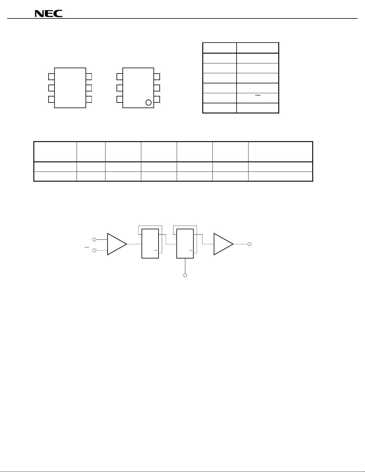
PIN CONNECTIONS
Pin No. Pin Name
µµµµ
PB1511TB
(Top View)
3
2
1
C2Z
4
5
6
4
5
6
(Bottom View)
3
2
1
1OUT
2GND
3SW
4IN
5IN
6V
CC
PRODUCT LINE-UP
2
CC
Part Number
PB1509 GV 5.0 2.2 to 5.5 50 to 700 50 to 800 50 to 1 000 8-pin SSOP
µ
PB1511TB 3.5 2.4 to 3.3 50 to 700 50 to 800
µ
Remark
This table shows the TYP. values of main parameters. Please refer to ELECTRICAL CHARACTERISTICS.
I
(mA)
V
(V)
CC
÷
in
f
(MHz)
4
÷
in
f
(MHz)
8
÷
in
f
(MHz)
−
6-pin super minimold
INTERNAL BLOCK DIAGRAM
Package
IN
IN
D
CLK
Q
Q
D
CLK
SW
Q
OUT
Q
2
Preliminary Data Sheet P14731EJ1V0DS00
Page 3
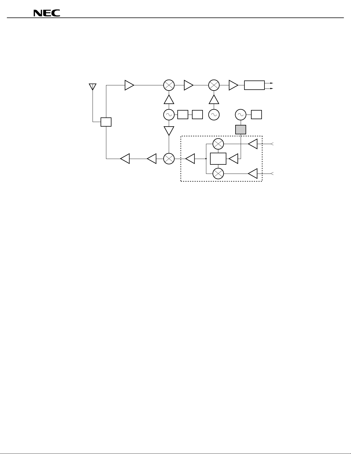
SYSTEM APPLICATION EXAMPLE
One of the example for usage
Low Noise Tr.
RX
SW
VCO
÷N PLL
DEMOD.
VCO
PLL
µ
÷N PB1511TB
µµµµ
PB1511TB
I
Q
I
Q
TX
PA
0°
Phase
Shifter
90°
Quadulator Modulator
This block diagram schematically shows the µPB1511TB’s location in one of the example application system. The
other applications are also acceptable for divider use.
Preliminary Data Sheet P14731EJ1V0DS00
3
Page 4

PIN EXPLANATIONS
Pin No. Symbol
Applied
Voltage
(V)
Functions and Explanation
µµµµ
PB1511TB
1OUT
2 GND 0 Ground pin. Ground pattern on the board should be formed as widely as possible
3 SW H/L Divide ratio control pin. Divide rati o can be determined by following applied level
4IN
5IN
6VCC2.4 to 3.3 Power supply pin. This pin m us t be equipped with bypass capaci tor (example:
Divided frequency output pin. This pin is designed as emitter follower output. This
pin can output 0.2 V
This pin should be coupled to load dev i ce with capacitor (example: 1 000 pF) for
DC cut.
to minimize ground impedance.
to these pins.
Divide ratio 1/2 1/4
These pins must be each equipped with bypass capacitor to m i ni m i ze their
impedance.
Signal input pin. This pin s houl d be coupled to signal source with capacitor
(example: 1 000 pF) for DC cut.
Signal input bypass pin. Thi s pin must be equipped with bypass capacitor
(example: 1 000 pF) to minimiz e ground i m pedance.
1 000 pF) to minimize ground impedance.
P-P
MIN. with 200 Ω load.
SW
HL
4
Preliminary Data Sheet P14731EJ1V0DS00
Page 5

ABSOLUTE MAXIMUM RATINGS
Parameter Symbol Conditions Ratings Unit
Supply Voltage V
Input Voltage V
Total Power Dissipat i on P
CC
TA = +25°C3.6V
in
TA = +25°C, SW pin 3.6 V
D
Mounted on double sided copper clad 50
50 × 1.6 mm epoxy glass PWB (T
+85°C)
Operating Ambient Temperature T
Storage Temperature T
A
stg
RECOMMENDED OPERATING CONDITIONS
Parameter Symbol MIN. TYP. MAX. Unit
Supply Voltage V
Operating Ambient Temperature T
CC
A
µµµµ
PB1511TB
200 mW
40 to +85
−
55 to +150
−
A
×
=
2.4 3.0 3.3 V
40 +25 +85
−
C
°
C
°
C
°
ELECTRICAL CHARACTERISTICS (TA = +25
Parameter Symbol Test Conditions M I N. TYP. MAX. Unit
Circuit Current I
Upper Limit Operating Frequency 1 f
Upper Limit Operating Frequency 2 f
Lower Limit Operating Frequency 1 f
Lower Limit Operating Frequency 2 f
Input Power 1 P
Input Power 2 P
Output Voltage V
Divide Ratio Control Input Hi gh V
Divide Ratio Control Input Low V
CC
in(U)1
in(U)2
in(L)1
in(L)2
in1
in2
out
No signals 3.1 3.5 4.1 mA
Pin = −20 to 0 dBm 500
Pin = −20 to −5 dBm @ ÷ 2
Pin = −20 to 0 dBm
Pin = −20 to −5 dBm
fin = 50 to 800 MHz
fin = 50 to 500 MHz
RL = 200
IH
IL
C, VCC = 3.0 V)
°°°°
@ ÷ 4
Ω
700
800
20
−
20
−
−
0.2 0.3
CC
0.7 × V
0.5
−
MHz
MHz
50 MHz
500 MHz
5dBm
0dBm
P-P
CC
V
+ 0.5 V
CC
V
× 0.3 V
V
Preliminary Data Sheet P14731EJ1V0DS00
5
Page 6

TEST CIRCUIT
High Impedance
µµµµ
PB1511TB
1 000 pF
IN
IN
4
1 000 pF
5
50 Ω
Signal Generator
3
SW
2
GND
Oscilloscope
50 Ω
Counter
(or Spectrum Analyzer)
PACKAGE DIMENSIONS
6-pin super minimold (Unit: mm)
1 000 pF
150 Ω
V
1
OUT
CC
6
1 000 pF
1 000 pF
Power Supply
Divide Ratio Setting
H1/2SW
L1/4
2.1±0.1
1.25±0.1
–0.05
+0.1
0.650.65
1.3
2.0±0.2
0.9±0.1
0.7
0 to 0.1
6
Preliminary Data Sheet P14731EJ1V0DS00
0.2
0.1 MIN.
–0
+0.1
0.15
Page 7

µµµµ
PB1511TB
NOTE ON CORRECT USE
(1) Observe precautions for handling because of electrostatic sensitive devices.
(2) Form a ground pattern as widely as possible to minimize ground impedance (to prevent undesired oscillation).
Keep the track length of the ground pins as short as possible.
(3) Connect a bypass capacitor (example: 1 000 pF) to the VCC pin.
RECOMMENDED SOLDERING CONDITIONS
This product should be soldered under the following recommended conditions. For soldering methods and
conditions other than those recommended below, contact your NEC sales representative.
Soldering Method Soldering Conditions Recommended Condition Symbol
Infrared Reflow Pac k age peak temperature: 235°C or below
Time: 30 seconds or less (at 210°C)
Count: 3, Exposure limi t: None
VPS Package peak temperature: 215°C or below
Time: 40 seconds or less (at 200°C)
Count: 3, Exposure limi t: None
Wave Soldering Soldering bath temperature: 260°C or below
Time: 10 seconds or less
Count: 1, Exposure limi t: None
Partial Heating Pin temperature: 300°C
Time: 3 seconds or less (per side of device)
Exposure limit: None
After opening the dry pack, keep it in a place below 25°C and 65% RH for the allowable storage period.
Note
Note
Note
Note
Note
IR35-00-3
VP15-00-3
WS60-00-1
–
Caution Do not use different soldering methods together (except for partial heating).
For details of recommended soldering conditions for surface mounting, refer to information document
SEMICONDUCTOR DEVICE MOUNTING TECHNOLOGY MANUAL (C10535E).
Preliminary Data Sheet P14731EJ1V0DS00
7
Page 8

µµµµ
PB1511TB
ATTENTION
OBSERVE PRECAUTIONS
FOR HANDLING
ELECTROSTATIC
SENSITIVE
DEVICES
NESAT (NEC Silicon Advanced Technology) is a trademark of NEC Corporation.
•
The information in this document is current as of June, 2000. The information is subject to change
without notice. For actual design-in, refer to the latest publications of NEC's data sheets or data
books, etc., for the most up-to-date specifications of NEC semiconductor products. Not all products
and/or types are available in every country. Please check with an NEC sales representative for
availability and additional information.
•
No part of this document may be copied or reproduced in any form or by any means without prior
written consent of NEC. NEC assumes no responsibility for any errors that may appear in this document.
•
NEC does not assume any liability for infringement of patents, copyrights or other intellectual property rights of
third parties by or arising from the use of NEC semiconductor products listed in this document or any other
liability arising from the use of such products. No license, express, implied or otherwise, is granted under any
patents, copyrights or other intellectual property rights of NEC or others.
•
Descriptions of circuits, software and other related information in this document are provided for illustrative
purposes in semiconductor product operation and application examples. The incorporation of these
circuits, software and information in the design of customer's equipment shall be done under the full
responsibility of customer. NEC assumes no responsibility for any losses incurred by customers or third
parties arising from the use of these circuits, software and information.
•
While NEC endeavours to enhance the quality, reliability and safety of NEC semiconductor products, customers
agree and acknowledge that the possibility of defects thereof cannot be eliminated entirely. To minimize
risks of damage to property or injury (including death) to persons arising from defects in NEC
semiconductor products, customers must incorporate sufficient safety measures in their design, such as
redundancy, fire-containment, and anti-failure features.
•
NEC semiconductor products are classified into the following three quality grades:
"Standard", "Special" and "Specific". The "Specific" quality grade applies only to semiconductor products
developed based on a customer-designated "quality assurance program" for a specific application. The
recommended applications of a semiconductor product depend on its quality grade, as indicated below.
Customers must check the quality grade of each semiconductor product before using it in a particular
application.
"Standard": Computers, office equipment, communications equipment, test and measurement equipment, audio
and visual equipment, home electronic appliances, machine tools, personal electronic equipment
and industrial robots
"Special": Transportation equipment (automobiles, trains, ships, etc.), traffic control systems, anti-disaster
systems, anti-crime systems, safety equipment and medical equipment (not specifically designed
for life support)
"Specific": Aircraft, aerospace equipment, submersible repeaters, nuclear reactor control systems, life
support systems and medical equipment for life support, etc.
The quality grade of NEC semiconductor products is "Standard" unless otherwise expressly specified in NEC's
data sheets or data books, etc. If customers wish to use NEC semiconductor products in applications not
intended by NEC, they must contact an NEC sales representative in advance to determine NEC's willingness
to support a given application.
(Note)
(1) "NEC" as used in this statement means NEC Corporation and also includes its majority-owned subsidiaries.
(2) "NEC semiconductor products" means any semiconductor product developed or manufactured by or for
NEC (as defined above).
M8E 00. 4
 Loading...