

Page 1
Features
■ Seven darlingtons per package
■ Extended temperature range:
-40 to 105°C
■ Output current 500mA per driver (600mA peak)
■ Output voltage 50V
■ Integrated suppression diodes for inductive
loads
■ Outputs can be paralleled for higher current
■ TTL/CMOS/PMOS/DTL Compatible inputs
■ Inputs pinned opposite outputs to simplify
layout
Description
The ULQ2001, ULQ2003 and ULQ2004 are high
voltage, high current darlington arrays each
containing seven open collector darlington pairs
with common emitters. Each channel rated at
500mA and can withstand peak currents of
600mA. Suppression diodes are included for
inductive load driving and the inputs are pinned
opposite the outputs to simplify board layout.
The versions interface to all common logic
families.
ULQ200XA/XD1
Seven darlington array
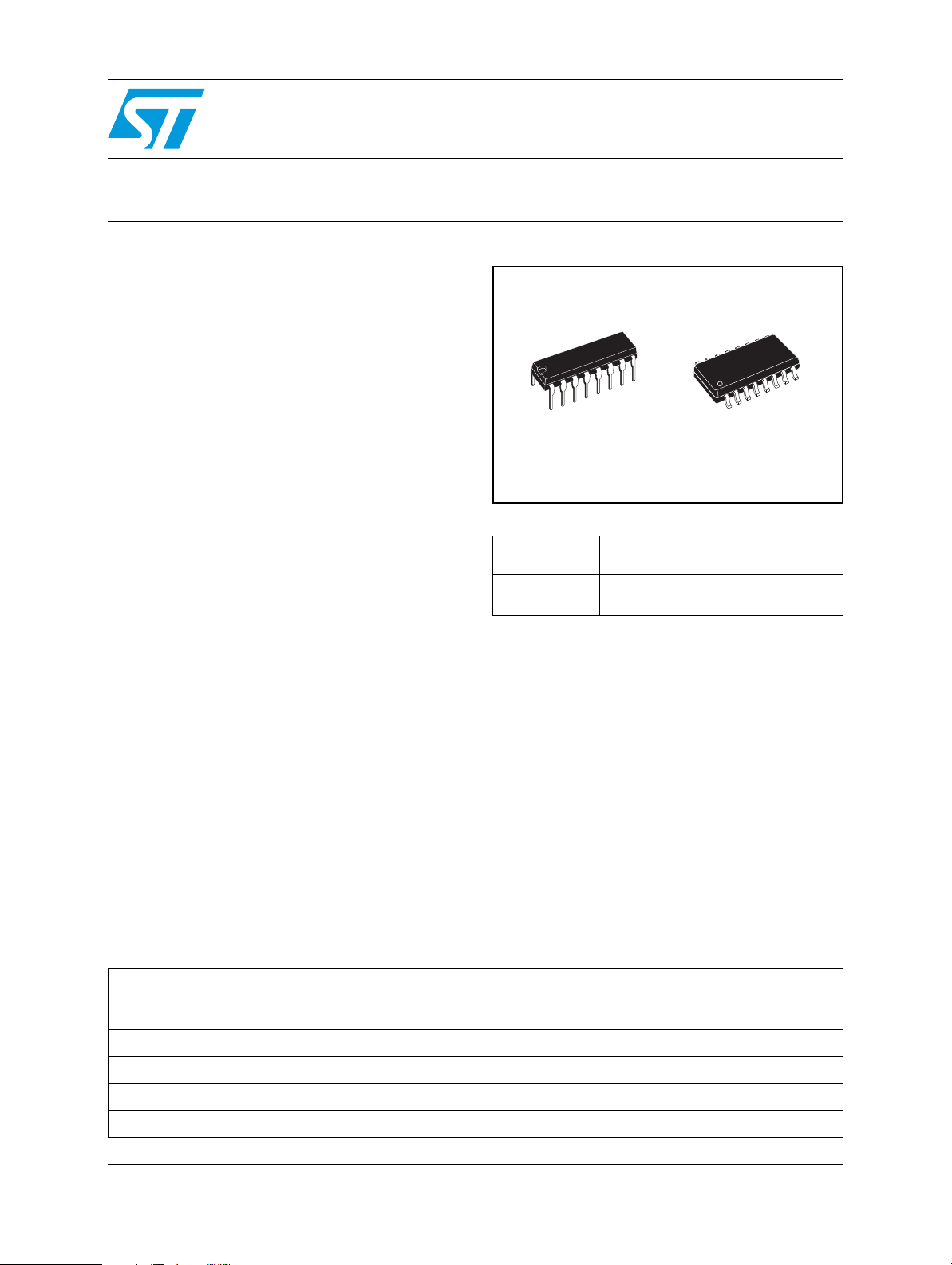
DIP-16
ULQ2001
ULQ2003 5V TTL, CMOS
ULQ2004 6–15V CMOS, PMOS
General purpose, DTL, TTL, PMOS,
CMOS
These versatile devices are useful for driving a
wide range of loads including solenoids, relays
DC motors, LED displays filament lamps, thermal
print-heads and high power buffers.
The ULQ2001A/2003A and 2004A are supplied in
16 pin plastic DIP packages with a copper leadframe to reduce thermal resistance. They are
available also in small outline package (SO-16) as
ULQ2003D1/2004D1.
SO16
(Narrow)
Order codes
Part numbers Packages
ULQ2001A DIP-16
ULQ2003A DIP-16
ULQ2004A DIP-16
ULQ2003D1013TR SO16 in Tape & Reel
ULQ2004D1013TR SO16 in Tape & Reel
May 2007 Rev. 3 1/13
www.st.com
13
Page 2

ULQ200XA/XD1
Contents
1 Diagram . . . . . . . . . . . . . . . . . . . . . . . . . . . . . . . . . . . . . . . . . . . . . . . . . . . 3
2 Pin configuration . . . . . . . . . . . . . . . . . . . . . . . . . . . . . . . . . . . . . . . . . . . 4
3 Maximum ratings . . . . . . . . . . . . . . . . . . . . . . . . . . . . . . . . . . . . . . . . . . . . 5
4 Electrical characteristics . . . . . . . . . . . . . . . . . . . . . . . . . . . . . . . . . . . . . 6
5 Test circuits . . . . . . . . . . . . . . . . . . . . . . . . . . . . . . . . . . . . . . . . . . . . . . . . 7
6 Package mechanical data . . . . . . . . . . . . . . . . . . . . . . . . . . . . . . . . . . . . . 9
7 Revision history . . . . . . . . . . . . . . . . . . . . . . . . . . . . . . . . . . . . . . . . . . . 12
2/13
Page 3
ULQ200XA/XD1 Diagram
1 Diagram
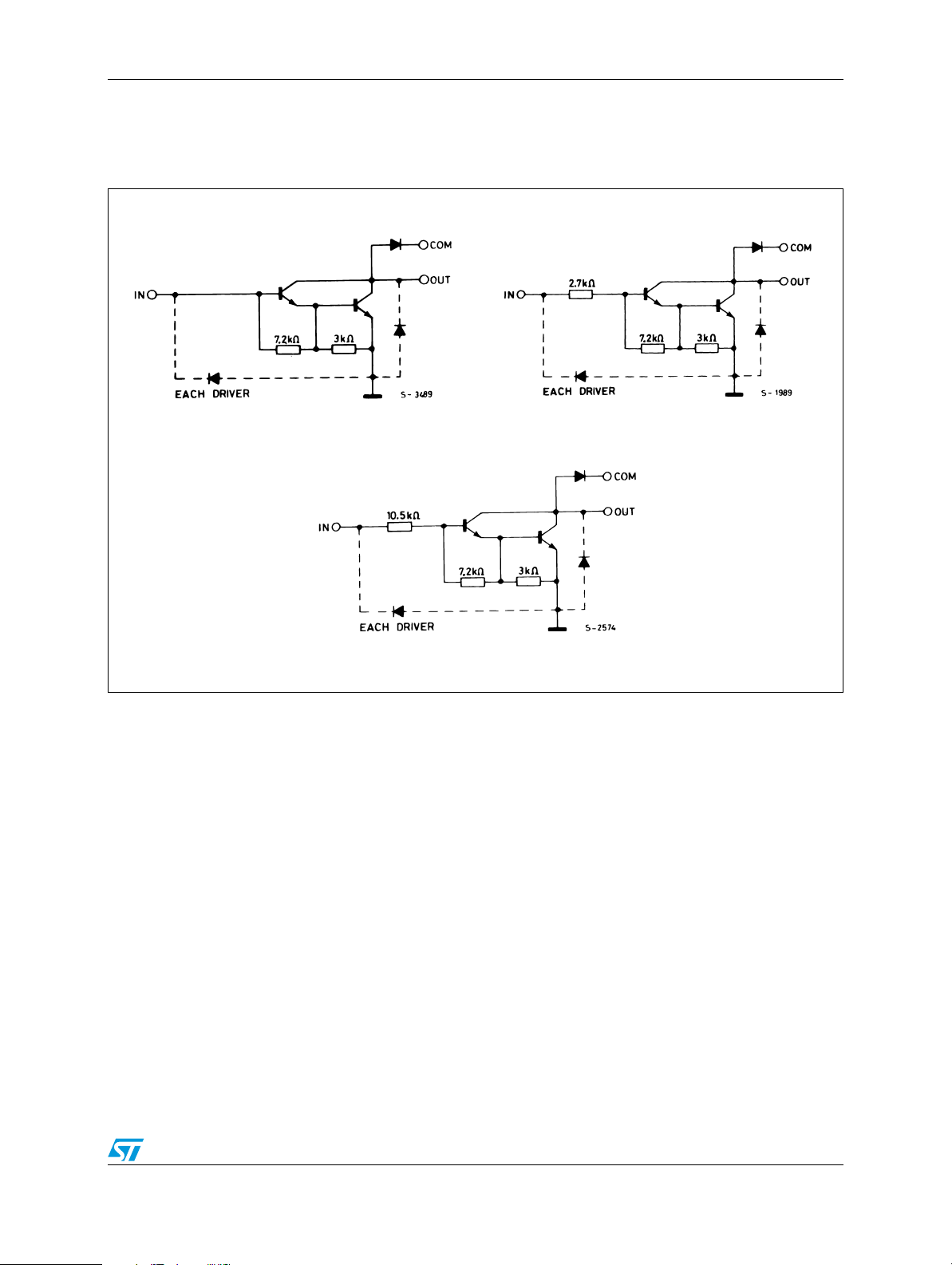
Figure 1. Schematic diagram
ULQ2001 (each driver) ULQ2003 (each driver)
ULQ2004 (each driver)
3/13
Page 4
Pin configuration ULQ200XA/XD1
2 Pin configuration
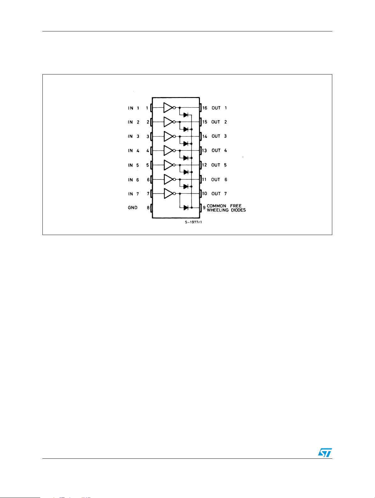
Figure 2. Pin connections (top view)
4/13
Page 5
ULQ200XA/XD1 Maximum ratings
3 Maximum ratings
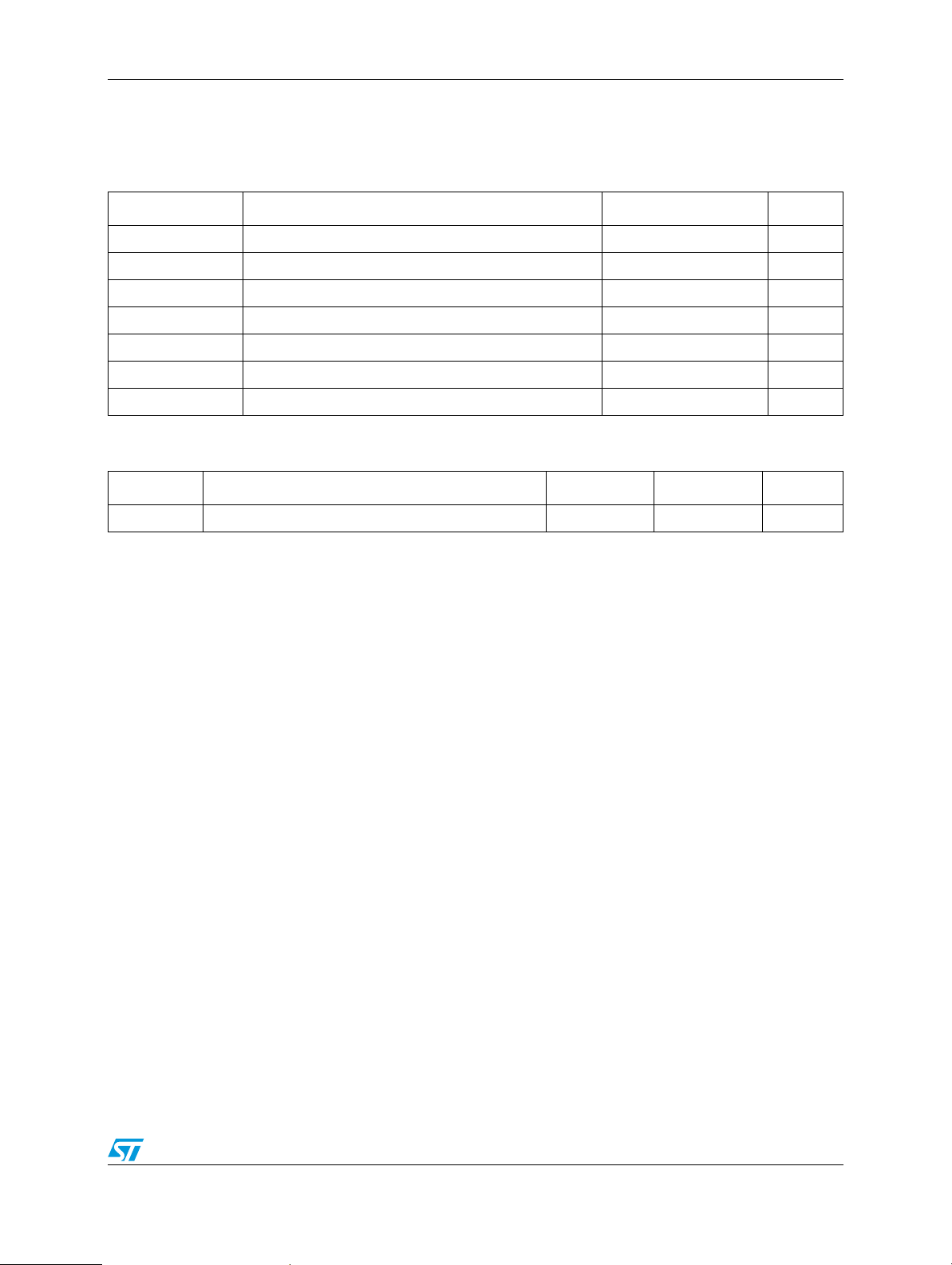
Table 1. Absolute maximum ratings
Symbol Parameter Value Unit
T
V
V
in
I
c
I
b
T
A
STG
T
J
o
Output voltage 50 V
Input voltage (for ULQ2003A/D1 - 2004A/D1) 30 V
Continuous collector current 500 mA
Continuous base current 25 mA
Operating ambient temperature range -40 to 105 ° C
Storage temperature range -55 to 150 ° C
Junction temperature 150 ° C
Table 2. Thermal Data
Symbol Parameter DIP-16 SO-16 Unit
R
thJA
Thermal resistance junction-ambient, Max. 70 120 ° C/W
5/13
Page 6
Electrical characteristics ULQ200XA/XD1
4 Electrical characteristics
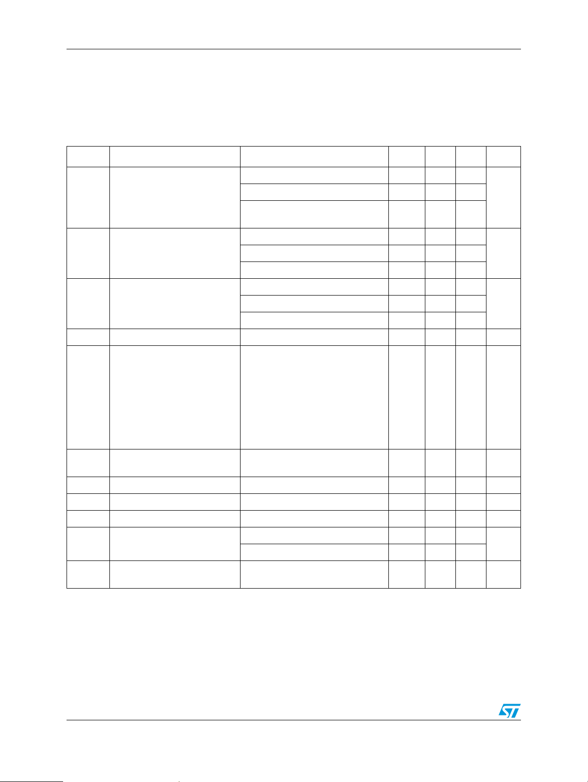
Table 3. Electrical characteristics
(T
= -40 to 105°C for DIP16 unless otherwise specified)
A
= 25 to 105°C for SO16 unless otherwise specified).
(T
J
Symbol Parameter Test conditions Min. Typ. Max. Unit
V
= 50V, (Figure 3.)50
CE
= 105°C, VCE= 50V (Figure 3.)100
T
I
CEX
V
CE(SAT)
I
I(ON)
I
I(OFF)
V
I(ON)
h
t
PLH
t
PHL
V
1. Guaranteed by design.
Output leakage current
Collector-emitter saturation
voltage (Figure 5.)
Input current (Figure 6.)
Input current (Figure 7.)T
Input voltage (Figure 8.)
DC Forward current gain
FE
(Figure 5.)
C
Input capacitance 15 25
I
Turn-on delay time 0.5 VI to 0.5V
Turn-off delay time 0.5 VI to 0.5V
Clamp diode leakage current
I
R
(Figure 9.)
Clamp diode forward voltage
F
(Figure 10.)
A
T
= 105°C for ULQ2004, VCE= 50V,
J
VI = 1V (Figure 4.)
500
IC = 100mA, IB = 250µA 0.9 1.1
= 200mA, IB= 350µA 1.1 1.3
C
= 350mA, IB= 500µA 1.3 1.6
I
C
for ULQ2003, V
= 12V 1 1.45
V
I
= 105°C, IC = 500µA 50 65 µA
A
= 3.85V 0.93 1.35
I
= 5V 0.35 0.5
I
for ULQ2003
I
= 200mA
C
= 250mA
I
C
IC = 300mA
2.4
2.7
3
for ULQ2004
= 125mA
I
C
IC = 200mA
IC = 275mA
= 350mA
I
C
for ULQ2001, VCE = 2V,
IC = 350mA
O
O
= 50V 50
V
R
= 105°C, VR = 50V 100
T
A
= 350mA 1.7 2 V
I
F
1000
0.25 1
0.25 1
5
6
7
8
(1)
(1)
(1)
µA
VI
mAfor ULQ2004, V
V
pF
µs
µs
µA
6/13
Page 7
ULQ200XA/XD1 Test circuits
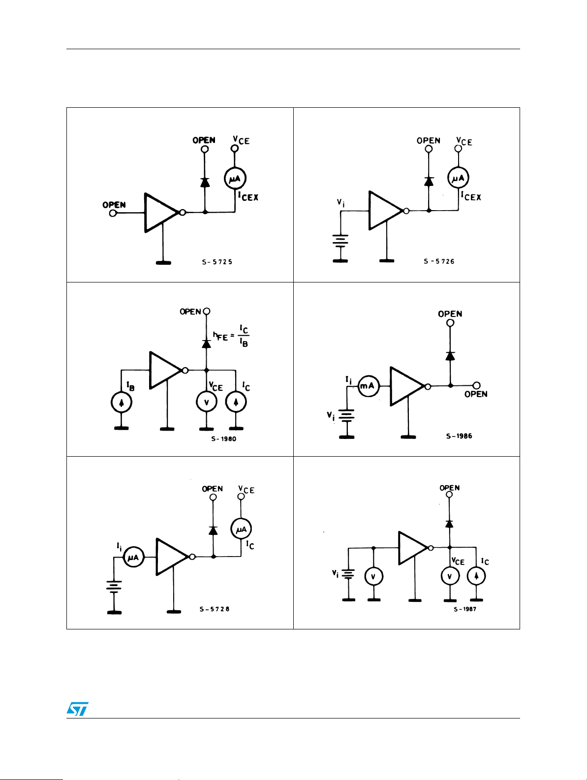
5 Test circuits
Figure 3. Figure 4.
Figure 5. Figure 6.
Figure 7. Figure 8.
7/13
Page 8
Test circuits ULQ200XA/XD1
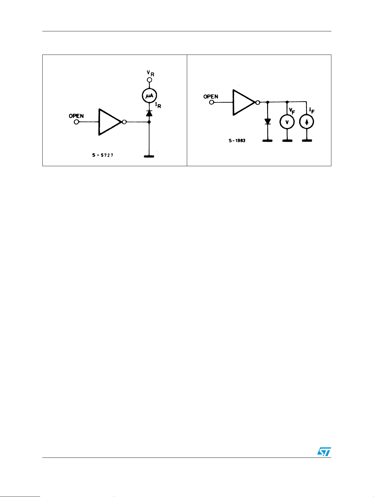
Figure 9. Figure 10.
8/13
Page 9

ULQ200XA/XD1 Package mechanical data
6 Package mechanical data
In order to meet environmental requirements, ST offers these devices in ECOPACK®
packages. These packages have a Lead-free second level interconnect. The category of
second Level Interconnect is marked on the package and on the inner box label, in
compliance with JEDEC Standard JESD97. The maximum ratings related to soldering
conditions are also marked on the inner box label. ECOPACK is an ST trademark.
ECOPACK specifications are available at: www.st.com.
9/13
Page 10
Package mechanical data ULQ200XA/XD1
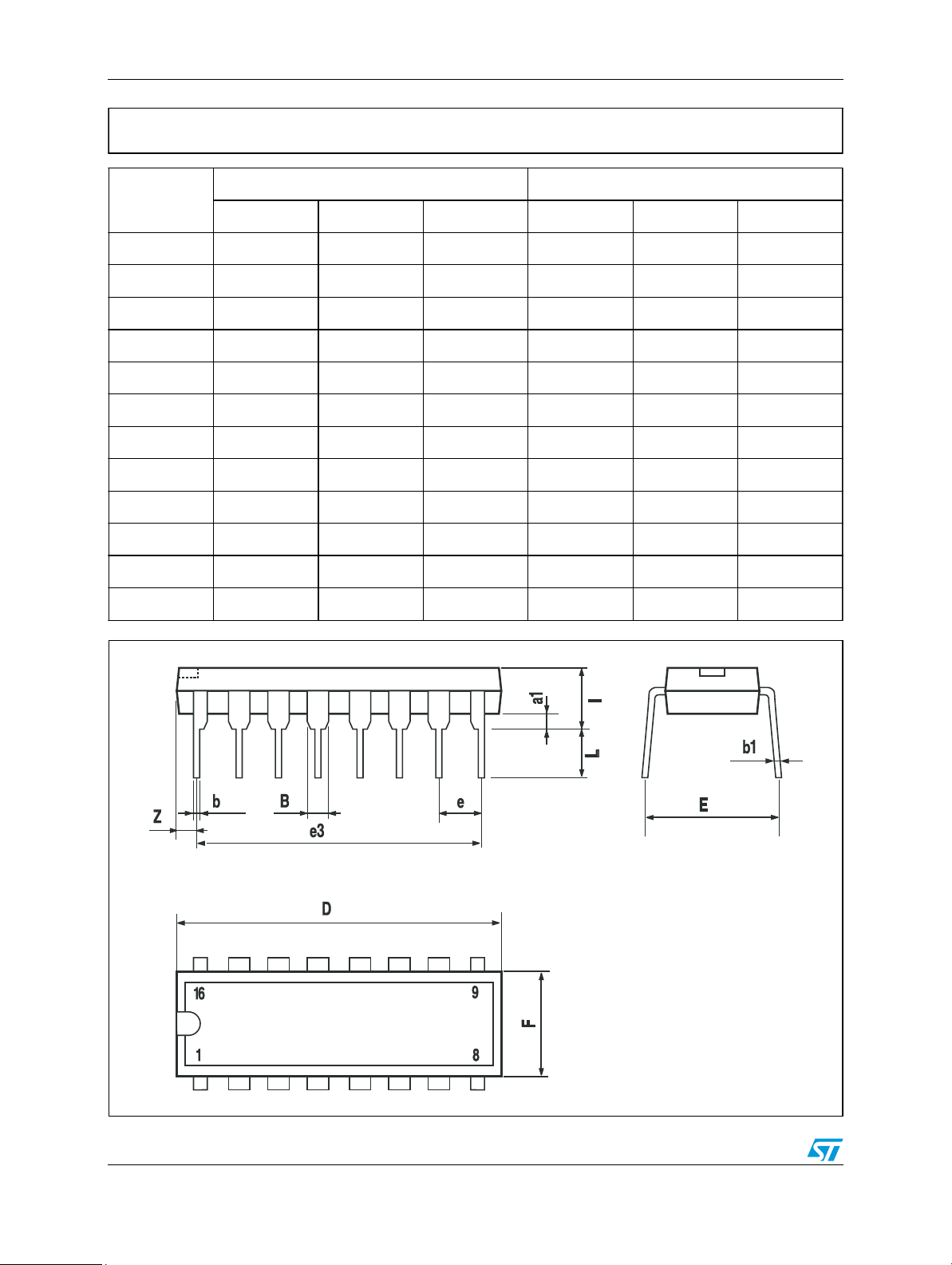
Plastic DIP-16 (0.25) MECHANICAL DATA
mm. inch
DIM.
MIN. TYP MAX. MIN. TYP. MAX.
a1 0.51 0.020
B 0.77 1.65 0.030 0.065
b 0.5 0.020
b1 0.25 0.010
D 20 0.787
E 8.5 0.335
e 2.54 0.100
e3 17.78 0.700
F 7.1 0.280
I 5.1 0.201
L 3.3 0.130
Z 1.27 0.050
10/13
P001C
Page 11
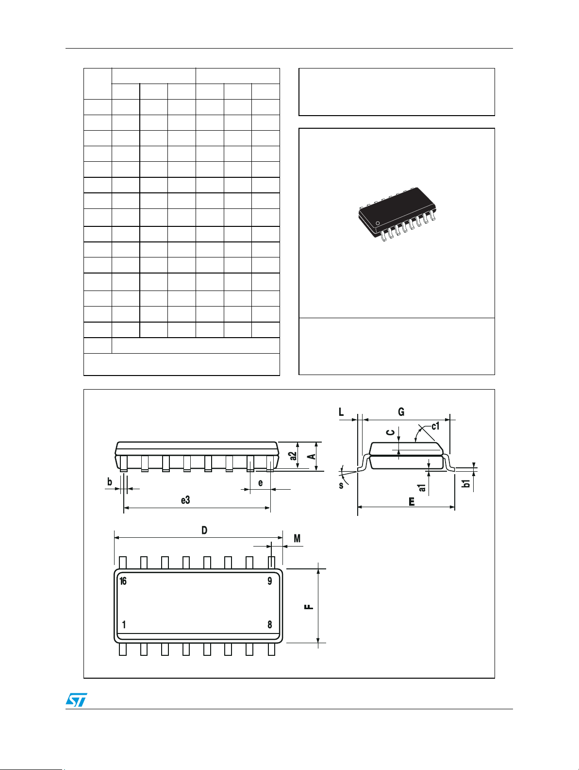
ULQ200XA/XD1 Package mechanical data
DIM.
A 1.75 0.069
a1 0.1 0.25 0.004 0.009
a2 1.6 0.063
b 0.35 0.46 0.014 0.018
b1 0.19 0.25 0.007 0.010
C 0.5 0.020
c1 45° (typ.)
(1)
D
E 5.8 6.2 0.228 0.244
e 1.27 0.050
e3 8.89 0.350
(1)
F
G 4.60 5.30 0.181 0.208
L 0.4 1.27 0.150 0.050
M 0.62 0.024
S8° (max.)
(1) "D" and "F" do not include mold flash or protrusio ns - Mold
flash or pro trusions sh all not exceed 0.15mm (.006inc.)
mm inch
MIN. TYP. MAX. MIN. TYP. MAX.
9.8 10 0.386 0.394
3.8 4.0 0.150 0.157
OUTLINE AND
MECHANICAL DATA
SO16 (Narrow)
0016020 D
11/13
Page 12
Revision history ULQ200XA/XD1
7 Revision history
Table 4. Revision history
Date Revision Changes
05-Dec-2006 2 Order codes has been updated and document has been reformatted.
23-May-2007 3 Order codes has been updated.
12/13
Page 13

ULQ200XA/XD1
Please Read Carefully:
Information in this document is provided solely in connection with ST products. STMicroelectronics NV and its subsidiaries (“ST”) reserve the
right to make changes, corrections, modifications or improvements, to this document, and the products and services described herein at any
time, without notice.
All ST products are sold pursuant to ST’s terms and conditions of sale.
Purchasers are solely responsible for the choice, selection and use of the ST products and services described herein, and ST assumes no
liability whatsoever relating to the choice, selection or use of the ST products and services described herein.
No license, express or implied, by estoppel or otherwise, to any intellectual property rights is granted under this document. If any part of this
document refers to any third party products or services it shall not be deemed a license grant by ST for the use of such third party products
or services, or any intellectual property contained therein or considered as a warranty covering the use in any manner whatsoever of such
third party products or services or any intellectual property contained therein.
UNLESS OTHERWISE SET FORTH IN ST’S TERMS AND CONDITIONS OF SALE ST DISCLAIMS ANY EXPRESS OR IMPLIED
WARRANTY WITH RESPECT TO THE USE AND/OR SALE OF ST PRODUCTS INCLUDING WITHOUT LIMITATION IMPLIED
WARRANTIES OF MERCHANTABILITY, FITNESS FOR A PARTICULAR PURPOSE (AND THEIR EQUIVALENTS UNDER THE LAWS
OF ANY JURISDICTION), OR INFRINGEMENT OF ANY PATENT, COPYRIGHT OR OTHER INTELLECTUAL PROPERTY RIGHT.
UNLESS EXPRESSLY APPROVED IN WRITING BY AN AUTHORIZED ST REPRESENTATIVE, ST PRODUCTS ARE NOT
RECOMMENDED, AUTHORIZED OR WARRANTED FOR USE IN MILITARY, AIR CRAFT, SPACE, LIFE SAVING, OR LIFE SUSTAINING
APPLICATIONS, NOR IN PRODUCTS OR SYSTEMS WHERE FAILURE OR MALFUNCTION MAY RESULT IN PERSONAL INJURY,
DEATH, OR SEVERE PROPERTY OR ENVIRONMENTAL DAMAGE. ST PRODUCTS WHICH ARE NOT SPECIFIED AS "AUTOMOTIVE
GRADE" MAY ONLY BE USED IN AUTOMOTIVE APPLICATIONS AT USER’S OWN RISK.
Resale of ST products with provisions different from the statements and/or technical features set forth in this document shall immediately void
any warranty granted by ST for the ST product or service described herein and shall not create or extend in any manner whatsoever, any
liability of ST.
ST and the ST logo are trademarks or registered trademarks of ST in various countries.
Information in this document supersedes and replaces all information previously supplied.
The ST logo is a registered trademark of STMicroelectronics. All other names are the property of their respective owners.
© 2007 STMicroelectronics - All rights reserved
STMicroelectronics group of companies
Australia - Belgium - Brazil - Canada - China - Czech Republic - Finland - France - Germany - Hong Kong - India - Israel - Italy - Japan -
Malaysia - Malta - Morocco - Singapore - Spain - Sweden - Switzerland - United Kingdom - United States of America
www.st.com
13/13
 Loading...