

Page 1

UCS1003-1/2/3
USB Port Power Controller with Charger Emulation
Features:
• Port Power Switch with Two Current Limit Behaviors
- 2.9V to 5.5V Source Voltage Range
- Up to 3.0A Current (2.85A typical) with
55 m On Resistance
- Overcurrent Trip or Constant Current Limiting
- Soft Turn-On Circuitry
- Selectable Current Limit
- UCS1003-1 has programmable Current Limit
via the SMBus 2.0/I
- Dynamic Thermal Management
- Undervoltage and Overvoltage Lockout
- Back-Drive, Back-Voltage Protection
- Latch or Auto-Recovery (Low-Test Current)
Fault Handling
- Selectable Active-High or -Low Power Switch
Enable
- BC1.2 V
Function
• Selectable/Automatic Cycling of Universal Serial
Bus (USB) Data Line Charger Emulation Profiles
- USB-IF BC1.2 Charging Downstream Port
(CDP) and Dedicated Charging Port (DCP)
modes, Chinese Telecommunications Industry
Standard YD/T 1591-2009 and most Apple
Inc., Samsung and RIM
- UCS1003-1 supports other Charger Emula-
tion Profiles as defined via the SMBus
2.0/I
- Supports 12W Charging Emulation
- USB 2.0 Compliant High-Speed Data Switch
(in Data Pass-Through, SDP and CDP modes)
- Nine preloaded charger emulation profiles for
maximum compatibility coverage of the
peripheral devices
- UCS1003-1 has one Custom-Programmable
Charger Emulation profile for portable device
support for fully host-controlled charger
emulation
• Supports Active Cables
• UCS1003-1 supports Self-Contained Current
Monitoring and Rationing for power-allocation
applications
• UCS1003-1 and UCS1003-3 have Low-Power
Attach Detection and Open-Drain (A_DET#) pin
• UCS1003-2 has Charging Active (CHRG#)
Open-Drain Pin
• Ultra-Low Power Sleep State
• Optional Split Supply Support for V
Low Power in System Standby states
2C™
BUS
protocol
2C™
protocol
Discharge Port Renegotiation
®
protocols standard
and VDD for
S
®
• Wake on Attach USB (UCS1003-1 and UCS1003-3)
• UCS1003-1 supports SMBus 2.0/I2C Communications
- Supports Block Write and Read
- Multiple SMBus Addresses
• Wide Operating Temperature Range: -40°C to +85°C
• IEC61000-4-2 8/15 kV Electrostatic Discharge
(ESD) Immunity
Description:
The UCS1003-1/2/3 family of devices provides a USB
port power switch for precise control of up to 3.0A
continuous current (2.85A typical) with Overcurrent
Limit (OCL), dynamic thermal management, latch or
Auto-Recovery (low-test current) fault handling,
selectable active-high or -low enable, undervoltage and
overvoltage lockout, back-drive protection and backvoltage protection.
Split supply support for V
power in system standby states. This gives batteryoperated applications (such as on-board computers)
the ability to detect attachments from a Sleep or Off
state. After the Attach Detection is flagged, the system
can decide to wake-up and/or provide charging.
In addition to Power Switching and Current Limiting
modes, the UCS1003-1/2/3 will automatically charge a
wide variety of portable devices, including USB-IF
BC1.2, YD/T-1591 (2009), most Apple Inc., Samsung
and RIM and many others. Nine preloaded charger
emulation profiles maximize the compatibility coverage
of the peripheral devices. Additionally, a customizable
charger emulation profile is available in UCS1003-1 to
accommodate unique existing and future portable
device handshaking/signature requirements.
The UCS1003-1 also provides current monitoring to
allow intelligent management of system power and
charge rationing for controlled delivery of current, regardless of the host power state. This is especially important
for battery-operated applications that want to provide
power and do not want to drain the battery excessively.
The UCS1003-1/2/3 is available in a 4 mm x 4 mm
20-pin QFN package.
and VDD is an option for low
S
Applications:
• Notebook and Netbook Computers
• Tablets and E-book readers
• Desktops and Monitors
• Docking Stations and Printers
• AC-DC Wall Adapters
2014 Microchip Technology Inc. DS200005346A-page 1
Page 2

UCS1003-1/2/3
D
MOUT
2
V
BUS1
V
BUS2
M1
D
MIN
D
PIN
SEL
ALERT#
VS1V
S2
V
DD
SMCLK/S0
GND
EM_EN
A_DET#
D
POUT
M2
EP
20119 18 17
3
4
14
13
12
11
678 9
21
5
10
15
16
COMM_SEL/I
LIM
PWR_EN
SMDATA/LATCH
* Includes Exposed Thermal Pad (EP); see Table 3-1.
D
MOUT
2
V
BUS1
V
BUS2
M1
D
MIN
D
PIN
SEL
ALERT#
VS1V
S2
V
DD
S0
GND
EM_EN
CHRG#
D
POUT
M2
EP
20119 18 17
3
4
14
13
12
11
6789
21
5
10
15
16
I
LIM
PWR_EN
LATCH
UCS1003-1
4x4 QFN*
UCS1003-2
4x4 QFN*
D
MOUT
2
V
BUS1
V
BUS2
M1
D
MIN
D
PIN
SEL
ALERT#
VS1V
S2
V
DD
S0
GND
EM_EN
A_DET#
D
POUT
M2
EP
20119 18 17
3
4
14
13
12
11
6789
21
5
10
15
16
I
LIM
PWR_EN
LATCH
UCS1003-3
4x4 QFN*
Package Type
DS200005346A-page 2 2014 Microchip Technology Inc.
Page 3

Block Diagram
Note 1: Available for UCS1003-1 only.
2: Available for UCS1003-2 only.
3: Available for UCS1003-3 only.
Charger Control,
Measurement,
OCL
Interface,
Logic
SMCLK (Note 1)/S0
SMDATA (Note 1)/LATCH
A_DET# (Note 1, Note 3)
ALERT#
Power
Switch
Temp
PWR_EN
D
POUT
D
MOUT
D
PIN
V
DD
V
S
V
BUS
D
MIN
GND
USB 2.0 HS Data Switch &
Charger Emulator
COMM_SEL (Note 1)
/I
LIM
Attach Detector
M1
M2
SEL
EM_EN
V
DD
V
DD
UVLO,
OVLO
CHRG# (Note 2)
UCS1003-1/2/3
2014 Microchip Technology Inc. DS200005346A-page 3
Page 4

UCS1003-1/2/3
NOTES:
DS200005346A-page 4 2014 Microchip Technology Inc.
Page 5

1.0 ELECTRICAL CHARACTERISTICS
Absolute Maximum Ratings †
UCS1003-1/2/3
Voltage on VDD, VS and V
Pull-Up Voltage (V
PULLUP
Data Switch Current (I
pins ....................................................................................................................-0.3 to 6V
BUS
) ...................................................................................................................-0.3 to VDD + 0.3V
HSW_ON
), Switch On...........................................................................................................±50 mA
Port Power Switch Current ..................................................................................................................... Internally limited
Data Switch Pin Voltage To Ground (D
POUT
PIN
Differential Voltage Across Open Data Switch (D
, D
POUT
MOUT
-D
, D
); (VDD powered or unpowered)....... -0.3 to VDD+0.3V
MIN
PIN
, D
MOUT
- D
MIN
, D
PIN
- D
POUT
, D
MIN
- D
MOUT
) .............V
DD
, D
Voltage on any Other Pin to Ground ................................................................................................... -0.3 to VDD + 0.3V
Current on any Other Pin......................................................................................................................................±10 mA
Package Power Dissipation ............................................................................................................................... Tab le 1 -1
Operating Ambient Temperature Range .....................................................................................................-40 to +125°C
Storage Temperature Range.......................................................................................................................-55 to +150°C
† Notice: Stresses above those listed under “Maximum Ratings” may cause permanent damage to the device. This is
a stress rating only and functional operation of the device at those or any other conditions above those indicated in the
operation listings of this specification is not implied. Exposure to maximum rating conditions for extended periods may
affect device reliability.
TABLE 1-1: POWER DISSIPATION SUMMARY
Board Package
High K
(see Note 1)
Low K
(see Note 1)
20-pin QFN
4x4 mm
20-pin QFN
4x4 mm
Note 1: Junction to ambient (
via design with a thermal landing soldered to the PCB ground plane with 0.3 mm (12 mil) diameter vias in
a 3x3 matrix (9 total) at 0.5 mm (20 mil) pitch. The board is multi-layer with 1-ounce internal power and
ground planes and 2-ounce copper traces on top and bottom. A Low K board is a two-layer board without
thermal via design with 2-ounce copper traces on the top and bottom.
De-Rating
JC
JA
Factor Above
+25°C
6°C/W 41°C/W 24.4 mW°/C 2193 mW 1095 mW 729 mW
6°C/W 60°C/W 16.67 mW°/C 1498 mW 748 mW 498 mW
) is dependent on the design of the thermal vias. A High K board uses a thermal
JA
TA<+25°C
Power
Rating
TA<+70°C
Power
Rating
TA<+85°C
Power
Rating
TABLE 1-2: ELECTRICAL CHARACTERISTICS
Electrica l Charact eristics: Unless otherwise specified, V
T
= -40°C to +85°C; all Typical values at VDD = VS = 5V, TA = +27°C.
A
Characteristic Sym. Min. Typ. Max. Unit Conditions
Power Supply
Supply Voltage V
Source Voltage V
DD
S
4.5 5 5.5 V Note 1
2.9 5 5.5 V Note 1
Note 1: For split supply systems using the Attach Detection feature, V
2: This parameter is ensured by design and not 100% tested.
3: This parameter is characterized, but not 100% production tested.
4: The current measurement full-scale range maximum value is 3.0A. However, the UCS1003-1 cannot report
values above I
LIM
(if I
BUS_R2MIN
I
LIM
) or above I
5: The Min and Max values represent the boundaries of a programmable range for UCS1003-1 only. Each value
in the range is typical.
2014 Microchip Technology Inc. DS200005346A-page 5
= 4.5V to 5.5V, VS = 2.9V to 5.5V, V
DD
must not exceed VDD+150mV.
S
BUS_R2MIN
(if I
BUS_R2MIN
> I
LIM
and I
PULLUP
1.68A).
LIM
= 3V to 5.5V,
Page 6

UCS1003-1/2/3
TABLE 1-2: ELECTRICAL CHARACTERISTICS (CONTINUED)
Electrica l Charact eristics: Unless otherwise specified, V
= -40°C to +85°C; all Typical values at VDD = VS = 5V, TA = +27°C.
T
A
Characteristic Sym. Min. Typ. Max. Unit Conditions
Supply Current in Active
(I
DD_ACTIVE
+ I
VS_ACT
)
Supply Current in Sleep
(I
DD_SLEEP
+ I
VS_SLEEP
)
Supply Current in Detect
(I
DD_DETECT
+ I
VS_DETECT
)
I
— 650 750 µA Average current I
ACTIVE
I
SLEEP
I
DETECT
— 5 15 µA Average current
— 185 — µA Average current,
Power-on Reset
Low Threshold V
V
S
Low Hysteresis V
V
S
V
Low Threshold V
DD
V
Low Hysteresis V
DD
S_UVLO
S_UVLO_HYST
DD_TH
DD_TH_HYST
—2.5— VV
—100— mVVS voltage decreasing
—4— VV
—500— mVVDD voltage decreasing
I/O Pins - SMCLK (UCS1003-1), SMDATA (UCS1003-1), EM_EN, M1, M2, PWR_EN, S0, LATCH, ALERT#, A_DET#
(UCS1003-1 and UCS1003-3), CHRG# (UCS1003-2) – DC Parameters
Output Low Voltage V
Input High Voltage V
Input Low Voltage V
Leakage Current I
LEAK
OL
IH
IL
——0.4 VI
2.0 — — V PWR_EN, EM_EN, M1, M2,
— — 0.8 V PWR_EN, EM_EN, M1, M2,
— — ±5 µA Powered or unpowered,
Interrupt Pins - AC Parameters
ALERT#, A_DET# Pin
t
BLANK
—25—ms
Blanking Time
ALERT# Pin
t
MASK
—5—ms
Interrupt Masking Time
SMBus/I2C™ Timing (UCS1003-1 only)
Input Capacitance C
Clock Frequency f
Spike Suppression t
Bus Free Time Stop-to-Start t
Start Setup Time t
Start Hold Time t
Stop Setup Time t
Data Hold Time t
SU:STA
HD:STA
SU:STO
HD:DAT
IN
SMB
SP
BUF
—5—pF
10 — 400 kHz
1.3 — — µs
0.6 — — µs
0.6 — — µs
0.6 — — µs
0 — — µs When transmitting to the
Note 1: For split supply systems using the Attach Detection feature, V
2: This parameter is ensured by design and not 100% tested.
3: This parameter is characterized, but not 100% production tested.
4: The current measurement full-scale range maximum value is 3.0A. However, the UCS1003-1 cannot report
values above I
LIM
(if I
BUS_R2MIN
I
LIM
) or above I
5: The Min and Max values represent the boundaries of a programmable range for UCS1003-1 only. Each value
in the range is typical.
= 4.5V to 5.5V, VS = 2.9V to 5.5V, V
DD
V
no portable device attached.
SINK_IO
SMDATA, ALERT#,
A_DET#, CHRG#
LATCH, S0, SMDATA, SMCLK
LATCH, S0, SMDATA, SMCLK
V
—50 nsNote 2
master
must not exceed VDD+150mV.
S
BUS_R2MIN
(if I
BUS_R2MIN
> I
LIM
= 3V to 5.5V,
PULLUP
V
PULLUP
voltage increasing
S
voltage increasing
DD
DD
= 8 mA
V
PULLUP
and I
1.68A).
LIM
DD
BUS
=0mA
DS200005346A-page 6 2014 Microchip Technology Inc.
Page 7

UCS1003-1/2/3
TABLE 1-2: ELECTRICAL CHARACTERISTICS (CONTINUED)
Electrica l Charact eristics: Unless otherwise specified, V
= -40°C to +85°C; all Typical values at VDD = VS = 5V, TA = +27°C.
T
A
Characteristic Sym. Min. Typ. Max. Unit Conditions
Data Hold Time t
Data Setup Time t
Clock Low Period t
Clock High Period t
Clock/Data Fall Time t
Clock/Data Rise Time t
Capacitive Load C
Timeout t
Idle Reset t
TIMEOUT
IDLE_RESET
HD:DAT
SU:DAT
LOW
HIGH
FALL
RISE
LOAD
0.3 — — µs When receiving from the
0.6 — — µs
1.3 — — µs
0.6 — — µs
——300nsMin = 20+0.1C
——300nsMin = 20+0.1C
— — 400 pF Per bus line, Note 2
25 — 35 ms Disabled by default, Note 2
350 — — µs Disabled by default, Note 2
High-Speed Dat a Swit ch
High-Speed Data Switch - DC Parameters
Switch Leakage Current I
HSW_OFF
Charger Resistance R
On Resistance R
On Resistance R
ON_HSW_1
Delta-On Resistance R
CHG
ON_HSW
ON_HSW
— ±0.5 — µA Switch open - D
—2—M D
—2— Switch closed, VDD = 5V
—5— Switch closed, VDD = 5V,
—±0.3— Switch closed, VDD = 5V,
High-Speed Data Switch - AC Parameters
DP, DM Capacitance to
C
HSW_ON
— 4 — pF Switch closed, VDD = 5V
Ground
D
, DM Capacitance to
P
C
HSW_OFF
— 2 — pF Switch open, VDD = 5V
Ground
Note 1: For split supply systems using the Attach Detection feature, V
2: This parameter is ensured by design and not 100% tested.
3: This parameter is characterized, but not 100% production tested.
4: The current measurement full-scale range maximum value is 3.0A. However, the UCS1003-1 cannot report
values above I
LIM
(if I
BUS_R2MIN
I
LIM
) or above I
5: The Min and Max values represent the boundaries of a programmable range for UCS1003-1 only. Each value
in the range is typical.
= 4.5V to 5.5V, VS = 2.9V to 5.5V, V
DD
master
Note 3
Note 3
D
to ground.
V
ground (see Figure 1-2),
BC1.2 DCP charger
emulation active
test current = 8 mA,
test voltage = 0.4V,
see Figure 1-2
test current = 8 mA,
test voltage = 3.0V,
see Figure 1-2
I
TST
see Figure 1-2
must not exceed VDD+150mV.
S
BUS_R2MIN
(if I
BUS_R2MIN
> I
LIM
to D
MIN
VS.
DD
or D
POUT
= 8 mA, V
and I
PULLUP
MOUT
MOUT
1.68A).
LIM
TST
= 3V to 5.5V,
ns,
LOAD
ns,
LOAD
PIN
to D
POUT
,
, or all four pins
to V
BUS
or
= 0 to 1.5V,
2014 Microchip Technology Inc. DS200005346A-page 7
Page 8

UCS1003-1/2/3
TABLE 1-2: ELECTRICAL CHARACTERISTICS (CONTINUED)
Electrica l Charact eristics: Unless otherwise specified, V
= -40°C to +85°C; all Typical values at VDD = VS = 5V, TA = +27°C.
T
A
Characteristic Sym. Min. Typ. Max. Unit Conditions
Turn-Off Time t
Turn-On Time t
HSW_OFF
HSW_ON
Propagation Delay t
Propagation Delay Skew t
Rise/Fall Time t
– DM Crosstalk X
D
P
Off Isolation O
PD
PD
F/R
TALK
IRR
— 400 — µs Time from state control
— 400 — µs Time from state control
—0.25— nsR
—25— psR
—10— nsR
—-40— dBR
—-30— dBR
-3 dB Bandwidth BW — 1100 — MHz R
To t al J it te r t
Skew of Opposite Transitions
t
J
SK(P)
—200— psR
—20— psR
of the Same Output
Port Power Switch
Port Power Switch - DC Parameter
Overvoltage Lockout V
On Resistance R
V
Leakage Current I
S
Back-Voltage Protection
LEAK_VS
V
S_OV
ON_PSW
BV_TH
—6— V
—55—m 4.75V < VS < 5.25V
— 2.2 — µA Sleep state into VS pin
—150— mVV
Threshold
Back-Drive Current I
BD_1
I
BD_2
—0 3 µAV
—0 2 µAV
Note 1: For split supply systems using the Attach Detection feature, V
2: This parameter is ensured by design and not 100% tested.
3: This parameter is characterized, but not 100% production tested.
4: The current measurement full-scale range maximum value is 3.0A. However, the UCS1003-1 cannot report
values above I
LIM
(if I
BUS_R2MIN
I
LIM
) or above I
5: The Min and Max values represent the boundaries of a programmable range for UCS1003-1 only. Each value
in the range is typical.
= 4.5V to 5.5V, VS = 2.9V to 5.5V, V
DD
(EM_EN, M1, M2) switch on to
switch off, R
C
(EM_EN, M1, M2) switch off to
switch on, R
C
f= 240MHz
V
Rise Time = Fall Time = 500 ps
at 480 Mbps (PRBS = 215–1)
V
Any powered power pin to any
unpowered power pin. Current
out of unpowered pin (Note 3)
Any powered power pin to any
unpowered power pin, except
for V
Power state and V
Active Power state. Current
out of unpowered pin (Note 3)
must not exceed VDD+150mV.
S
BUS_R2MIN
(if I
BUS_R2MIN
> I
LIM
PULLUP
TERM
=5pF
LOAD
TERM
=5pF
LOAD
=50, C
TERM
=50, C
TERM
=50, C
TERM
=50, C
TERM
=50, C
TERM
=50, C
TERM
DPOUT=VDMOUT
=50, C
TERM
=50, C
TERM
> VS,
BUS
> V
S
S_UVLO
< V
DD
< V
DD
and I
DD
DD_TH
DD_TH
to V
1.68A).
LIM
,
,
BUS
= 3V to 5.5V,
=50,
=50,
=5pF
LOAD
=5pF
LOAD
=5pF
LOAD
=5pF
LOAD
=5pF,
LOAD
=5pF,
LOAD
= 350 mV DC
=5pF,
LOAD
=5pF
LOAD
in Detect
to V
S
BUS
in
DS200005346A-page 8 2014 Microchip Technology Inc.
Page 9

UCS1003-1/2/3
TABLE 1-2: ELECTRICAL CHARACTERISTICS (CONTINUED)
Electrica l Charact eristics: Unless otherwise specified, V
= -40°C to +85°C; all Typical values at VDD = VS = 5V, TA = +27°C.
T
A
Characteristic Sym. Min. Typ. Max. Unit Conditions
Selectable Current Limits I
Pin Wake Time t
SMBus Wake Time t
Idle Sleep Time t
PIN_WAKE
SMB_WAKE
IDLE_SLEEP
Thermal Regulation Limit T
LIM1
I
LIM2
I
LIM3
I
LIM4
I
LIM5
I
LIM6
I
LIM7
I
LIM8
REG
—570— mAI
—1000— I
—1130— I
—1350— I
—1680—
—2050—
—2280—
2700 2850 3000 I
—3—ms
—4—msUCS1003-1 only
—200— msUCS1003-1 only
— 110 — °C Die Temperature at which
Note 1: For split supply systems using the Attach Detection feature, V
2: This parameter is ensured by design and not 100% tested.
3: This parameter is characterized, but not 100% production tested.
4: The current measurement full-scale range maximum value is 3.0A. However, the UCS1003-1 cannot report
values above I
LIM
(if I
BUS_R2MIN
I
LIM
) or above I
5: The Min and Max values represent the boundaries of a programmable range for UCS1003-1 only. Each value
in the range is typical.
= 4.5V to 5.5V, VS = 2.9V to 5.5V, V
DD
LIM
(UCS1003-1 only)
I
LIM
(UCS1003-2/3)
(minimum mA setting)
LIM
(UCS1003-1 only)
I
LIM
(UCS1003-2/3)
LIM
(UCS1003-1 only)
I
LIM
(UCS1003-2/3)
LIM
(UCS1003-1 only)
I
LIM
(UCS1003-2/3)
I
LIM
(UCS1003-1 only)
I
LIM
(UCS1003-2/3)
I
LIM
(UCS1003-1 only)
I
LIM
(UCS1003-2/3)
I
LIM
(UCS1003-1 only)
I
LIM
(UCS1003-2/3)
LIM
(UCS1003-1 only)
I
LIM
(UCS1003-2/3)
current limit will be reduced
must not exceed VDD+150mV.
S
BUS_R2MIN
(if I
BUS_R2MIN
> I
LIM
PULLUP
Resistor = 0 or 47 k
Resistor = 47 k
Resistor = 10 k or 56 k
Resistor = 56 k
Resistor = 12 k or 68 k
Resistor = 68 k
Resistor = 15 k or 82 k
Resistor = 82 k
Resistor = 18 k or 100 k
Resistor = 100 k
Resistor = 22 k or 120 k
Resistor = 120 k
Resistor = 27 k or 150 k
Resistor = 150 k
Resistor = 33 k or V
Resistor = V
and I
1.68A).
LIM
= 3V to 5.5V,
DD
DD
2014 Microchip Technology Inc. DS200005346A-page 9
Page 10

UCS1003-1/2/3
TABLE 1-2: ELECTRICAL CHARACTERISTICS (CONTINUED)
Electrica l Charact eristics: Unless otherwise specified, V
= -40°C to +85°C; all Typical values at VDD = VS = 5V, TA = +27°C.
T
A
Characteristic Sym. Min. Typ. Max. Unit Conditions
Thermal Regulation
T
REG_HYST
—10— °CHysteresis for t
Hysteresis
Thermal Shutdown Threshold T
Thermal Shutdown Hysteresis T
TSD_HYST
Auto-Recovery Test Current I
Auto-Recovery Test Voltage V
Discharge Impedance R
DISCHARGE
TSD
TEST
TEST
— 135 — °C Die temperature at which port
— 35 — °C After shutdown due to
— 190 — mA Portable device attached,
— 750 — mV Portable device attached,
—100—
Port Power Switch - AC Parameters
Turn-On Delay t
Turn-Off Time t
Turn-Off Time t
Turn-Off Time t
V
Output Rise Time t
BUS
OFF_PSW_INA
OFF_PSW_ERR
OFF_PSW_ERR
Soft Turn-on Rate I
Temperature Update Time t
DC_TEMP
ON_PSW
R_BUS
BUS/t
— 0.75 — ms PWR_EN active toggle to
— 0.75 — ms PWR_EN inactive toggle to
— 1 — ms Overcurrent Error, V
— 100 — ns TSD or Back-drive Error to
— 1.1 — ms Measured from 10% to 90% of
—100—mA/µs
— 200 — ms Programmable (UCS1003-1
Note 1: For split supply systems using the Attach Detection feature, V
2: This parameter is ensured by design and not 100% tested.
3: This parameter is characterized, but not 100% production tested.
4: The current measurement full-scale range maximum value is 3.0A. However, the UCS1003-1 cannot report
values above I
LIM
(if I
BUS_R2MIN
I
LIM
) or above I
5: The Min and Max values represent the boundaries of a programmable range for UCS1003-1 only. Each value
in the range is typical.
= 4.5V to 5.5V, VS = 2.9V to 5.5V, V
DD
functionality. Temperature
must drop by this value before
I
LIM
operation
power switch will turn off
T
temperature drop required
before port power switch can
be turned on again
V
V
Die Temp < T
Programmable (UCS1003-1
only), 250-1000 mV, default
listed
switch on time, V
not active
switch off time
C
Error, or Discharge Error to
switch off, C
switch off, C
V
I
LIM
only) 200-1600 ms, default
listed
must not exceed VDD+150mV.
S
BUS_R2MIN
(if I
BUS_R2MIN
> I
LIM
PULLUP
value restored to normal
being reached, die
TSD
= 0V, Die Temp < T
BUS
= 0V before application,
BUS
TSD
= 120 μF
BUS
BUS
BUS
BUS
, C
LOAD
= 220 μF,
= 1.0A
and I
1.68A).
LIM
= 3V to 5.5V,
REG
TSD
discharge
BUS
Min
BUS
= 120 μF
= 120 μF
DS200005346A-page 10 2014 Microchip Technology Inc.
Page 11

UCS1003-1/2/3
TABLE 1-2: ELECTRICAL CHARACTERISTICS (CONTINUED)
Electrica l Charact eristics: Unless otherwise specified, V
= -40°C to +85°C; all Typical values at VDD = VS = 5V, TA = +27°C.
T
A
Characteristic Sym. Min. Typ. Max. Unit Conditions
Short Circuit Response Time t
Short Circuit Detection Time t
SHORT_LIM
SHORT
Latched Mode Cycle Time t
Auto-Recovery Mode
t
UL
CYCLE
— 1.5 — µs Time from detection of short to
— 6 — ms Time from detection of short to
— 7 — ms From PWR_EN edge transition
— 25 — ms Time delay before error
Cycle Time
Auto-Recovery Delay t
Discharge Time t
DISCHARGE
RST
— 20 — ms Portable device attached,
— 200 — ms Amount of time discharge
Port Power Switch Operation With Trip Mode Current Limiting
Region 2 Current Keep-Out I
Minimum V
Allowed at
BUS
BUS_R2MIN
V
BUS_MIN
—0.12— A
1.5 2.0 2.25 V
Output
Port Power Switch Operation with Constant Current Limiting (Variable Slope)
Region 2 Current Keep-Out I
Minimum V
Allowed at
BUS
BUS_R2MIN
V
BUS_MIN
—1.68— A
1.5 2.0 2.25 V
Output
Current Measurement (UCS1003-1 only) - DC
Current Measurement Range I
Reported Current
BUS_M
D
IBUS_M
0 — 2988.6 mA Range 0-255 LSB (see Note 4)
— 11.72 — mA 1 LSB
Measurement Resolution
Current Measurement
Accuracy
—±2— %180mA < I
—±2—LSBI
Current Measurement (UCS1003-1 only) - AC
Sampling Rate — 500 — µs
Note 1: For split supply systems using the Attach Detection feature, V
2: This parameter is ensured by design and not 100% tested.
3: This parameter is characterized, but not 100% production tested.
4: The current measurement full-scale range maximum value is 3.0A. However, the UCS1003-1 cannot report
values above I
LIM
(if I
BUS_R2MIN
I
LIM
) or above I
5: The Min and Max values represent the boundaries of a programmable range for UCS1003-1 only. Each value
in the range is typical.
= 4.5V to 5.5V, VS = 2.9V to 5.5V, V
DD
current limit applied. No C
applied
port power switch disconnect
and ALERT# pin assertion.
from inactive to active to begin
error recovery
condition check
Programmable (UCS1003-1
only) 10-25 ms, default listed
V
this time
Programmable (UCS1003-1
only) 10-25 ms, default listed
resistor applied
Programmable (UCS1003-1
only) 100-400 ms, default
listed
BUS
must not exceed VDD+150mV.
S
BUS_R2MIN
(if I
BUS_R2MIN
> I
LIM
PULLUP
must be V
BUS
< 180 mA
and I
LIM
< I
BUS
1.68A).
= 3V to 5.5V,
BUS
after
TEST
LIM
2014 Microchip Technology Inc. DS200005346A-page 11
Page 12

UCS1003-1/2/3
TABLE 1-2: ELECTRICAL CHARACTERISTICS (CONTINUED)
Electrica l Charact eristics: Unless otherwise specified, V
= -40°C to +85°C; all Typical values at VDD = VS = 5V, TA = +27°C.
T
A
Characteristic Sym. Min. Typ. Max. Unit Conditions
Charge Rationing (UCS1003-1 only) - DC
Accumulated Current
—±4.5— %
Measurement Accuracy
Charge Rationing (UCS1003-1 only) - AC
Current Measurement Update
t
PCYCLE
—1— s
Time
Attach/Removal Detection
V
BUS
On Resistance R
Leakage Current I
Current Limit I
ON_BYP
LEAK_BYP
DET_CHG
I
BUS_BYP
/
—50—
— — 3 µA Switch off, Note 2
—2—mAV
Attach/Removal Detection - DC
Attach Detection Threshold I
Primary Removal Detection
I
REM_QUAL_ACT
DET_QUAL
— 800 — µA Programmable (UCS1003-1
— 700 — µA Programmable (UCS1003-1
Threshold
I
REM_QUAL_DET
— 800 — µA Programmable (UCS1003-1
Attach/Removal Detection - AC
Attach Detection Time t
Removal Detection Time t
Allowed Charge Time t
DET_QUAL
REM_QUAL
DET_CHARGE
— 100 — ms Time from Attach to A_DET#
—1000— ms
—800— msC
Charger Emulation Profile
General Emulation - DC
Charging Current Threshold I
BUS_CHG
— 46.9 — mA Default value for UCS1003-1
—175.8— mAUCS1003-2 and UCS1003-3
Charging Current
I
BUS_CHG_RNG
11.72 — 175.8 mA Note 5
Threshold Range
Note 1: For split supply systems using the Attach Detection feature, V
2: This parameter is ensured by design and not 100% tested.
3: This parameter is characterized, but not 100% production tested.
4: The current measurement full-scale range maximum value is 3.0A. However, the UCS1003-1 cannot report
values above I
LIM
(if I
BUS_R2MIN
I
LIM
) or above I
5: The Min and Max values represent the boundaries of a programmable range for UCS1003-1 only. Each value
in the range is typical.
= 4.5V to 5.5V, VS = 2.9V to 5.5V, V
DD
Bypass - DC
must not exceed VDD+150mV.
S
BUS_R2MIN
(if I
BUS_R2MIN
> I
PULLUP
= 5V and V
DD
only) 200–1000 µA, default
listed
only) 100–900 µA, default
listed, Active Power state
only) 200–1000 µA, default
listed, Detect Power state (see
Section 8 .4 “Removal
Detection”)
assert (UCS1003-1 and
UCS1003-3 only)
= 500 µF maximum,
BUS
Programmable 200–2000 ms,
default listed
LIM
and I
1.68A).
LIM
= 3V to 5.5V,
> 4.75V
BUS
DS200005346A-page 12 2014 Microchip Technology Inc.
Page 13

UCS1003-1/2/3
TABLE 1-2: ELECTRICAL CHARACTERISTICS (CONTINUED)
Electrica l Charact eristics: Unless otherwise specified, V
= -40°C to +85°C; all Typical values at VDD = VS = 5V, TA = +27°C.
T
A
Characteristic Sym. Min. Typ. Max. Unit Conditions
DP-DM Shunt Resistor Value R
Response Magnitude
SX_RXMAG_DVDR
DCP_RES
——200 Connected between D
93 — 200 k Note 5
(voltage divider option
resistance range)
Resistor Ratio Range
SX_RATIO 0.25 — 0.66 V/V Note 5
(voltage divider option)
Resistor Ratio Accuracy
SX_RATIO_ ACC
— ±0.5 — % Average over range
(voltage divider option)
Response Magnitude
SX_RXMAG_RES
1.8 — 150 k Note 5
(resistor option range)
Internal Resistor Tolerance
(resistor option)
Response Magnitude
SX_RXMAG_RES
_ACC
SX_RXMAG_VOLT
— ±10 — % Average over range
0.4 — 2.2 V Note 5
(voltage option range)
Voltage Option Accuracy
Voltage Option Accuracy
Voltage Option Accuracy
Voltage Option Output
Response Magnitude
SX_RXMAG_VOLT
_ACC
SX_RXMAG_VOLT
_ACC_ 150
SX_RXMAG_VOLT
_ACC_ 250
SX_RXMAG_VOLT
_BC
— ±1 — % No load, average over range
— -6 — % 150 µA load,
— -10 — % 250 µA load,
0.5 — — V D
SX_PUPD 10 — 150 µA SX_RXMAG_VOLT = 0
(Zero Volt Option Range)
Pull-Down Current Accuracy
Pull-Down Current
Stimulus Voltage
SX_PUPD
_ACC_3p6
SX_PUPD
_ACC_BC
—±5— %D
50 — — µA Setting = 100 µA
SX_TH 0.3 — 2.2 V Note 5
Threshold Range
Stimulus Voltage Accuracy SX_TH_ ACC — ±2 — % Average over range
Stimulus Voltage Accuracy
SX_TH_ACC_BC
0.25 — — V At SX_TH = 0.3V, Note 3
General Emulation - AC
Emulation Reset Time t
Emulation Reset Time Range
t
EM_RESET_ RNG
Emulation Timeout Range t
EM_RESET
EM_ TIMEOUT
—50—msDefault
50 — 175 ms Note 5
0.8 — 12.8 s Note 5
Note 1: For split supply systems using the Attach Detection feature, V
2: This parameter is ensured by design and not 100% tested.
3: This parameter is characterized, but not 100% production tested.
4: The current measurement full-scale range maximum value is 3.0A. However, the UCS1003-1 cannot report
values above I
LIM
(if I
BUS_R2MIN
I
LIM
) or above I
5: The Min and Max values represent the boundaries of a programmable range for UCS1003-1 only. Each value
in the range is typical.
= 4.5V to 5.5V, VS = 2.9V to 5.5V, V
DD
and D
0V < D
average over range
average over range
Note 3
Note 5
Compliance voltage
D
Compliance voltage, Note 3
must not exceed VDD+150mV.
S
BUS_R2MIN
(if I
BUS_R2MIN
> I
LIM
= 3V to 5.5V,
PULLUP
,
MOUT
= D
POUT
= 0.6V, 250 µA load,
MOUT
or D
POUT
POUT
and I
or D
LIM
MOUT
MOUT
1.68A).
MOUT
POUT
< 3V
= 3.6V
= 0.15V
2014 Microchip Technology Inc. DS200005346A-page 13
Page 14
UCS1003-1/2/3
TABLE 1-2: ELECTRICAL CHARACTERISTICS (CONTINUED)
Electrica l Charact eristics: Unless otherwise specified, V
= -40°C to +85°C; all Typical values at VDD = VS = 5V, TA = +27°C.
T
A
Characteristic Sym. Min. Typ. Max. Unit Conditions
Stimulus Delay,
t
STIM_DEL
0 — 100 ms Note 5
SX_TD Range
Emulation Delay t
RES_EM
— — 0.5 s Time from set impedance to
Note 1: For split supply systems using the Attach Detection feature, V
2: This parameter is ensured by design and not 100% tested.
3: This parameter is characterized, but not 100% production tested.
4: The current measurement full-scale range maximum value is 3.0A. However, the UCS1003-1 cannot report
values above I
LIM
(if I
BUS_R2MIN
I
LIM
) or above I
5: The Min and Max values represent the boundaries of a programmable range for UCS1003-1 only. Each value
in the range is typical.
= 4.5V to 5.5V, VS = 2.9V to 5.5V, V
DD
impedance appears on D
Note 3
must not exceed VDD+150mV.
S
BUS_R2MIN
(if I
BUS_R2MIN
> I
LIM
and I
PULLUP
1.68A).
LIM
= 3V to 5.5V,
P/DM
,
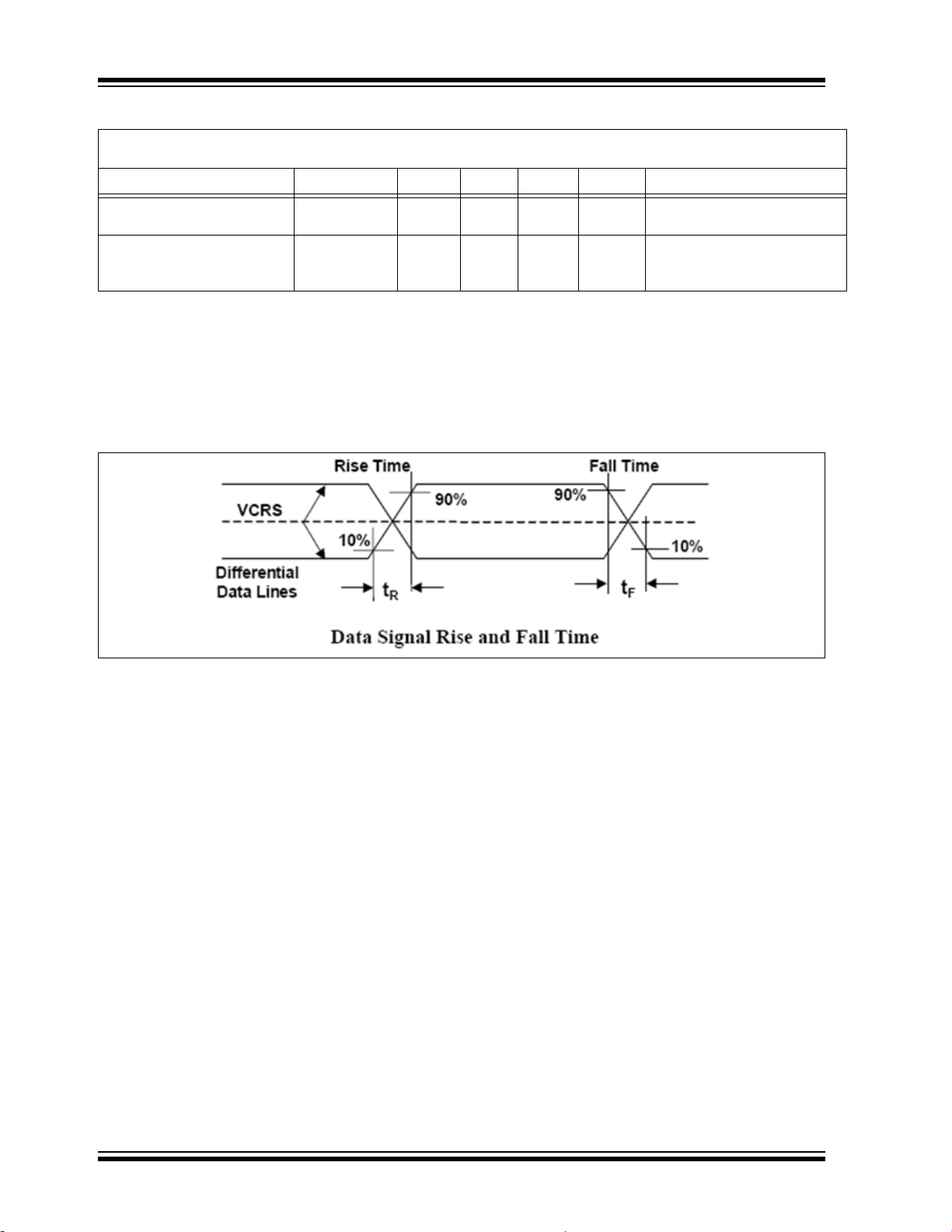
FIGURE 1-1: USB Rise Time/Fall Time Measurement.
DS200005346A-page 14 2014 Microchip Technology Inc.
Page 15

UCS1003-1/2/3
D
PIN
D
POUT
R
CHG
V
BUS
V
TST
R
CHG
I
TST
D
MIN
R
CHG
V
BUS
V
TST
R
CHG
I
TST
D
MOUT
FIGURE 1-2: Description of DC Terms.
TABLE 1-3: TEMPERATURE SPECIFICATIONS
Parameters Sym Min Typ Max Units Conditions
Temperature Ranges
Operating Temperature Range T
Storage Temperature Range T
Thermal Package Resistances - see Table 1-1
-40 — +85 °C
A
-55 — +150 °C
A
2014 Microchip Technology Inc. DS200005346A-page 15
Page 16

UCS1003-1/2/3
NOTES:
DS200005346A-page 16 2014 Microchip Technology Inc.
Page 17

UCS1003-1/2/3
-1
0
1
2
3
4
5
6
-1
0
1
2
3
4
5
6
0246810
VS= VDD= 5V
I
LIM
= 3A max. (2.85A typical), short applied at 2 ms
ALERT #
I
BUS
V
BUS
0
1
2
3
4
5
6
0
1
2
3
4
5
6
0
5
010203040
50
V
DD
ALERT# Pin
I
BUS
Current
Time (ms)
Voltage (V)Current (A) Voltage (V)
VS=VDD= 5V, short applied at 16 ms
-2
-1
0
1
2
3
4
5
6
02040
-2
0
2
4
6
8
10
12
14
Voltage (V)
VS=VDD= 5V,
I
LIM
= 2.05A (typical),
short applied at 17.2 μs
V
I
BUS
-1
0
1
2
3
4
5
6
0 100 200 300 400 500
Voltage (V)
V
BUS
EM_EN
VS= VDD= 5V
M2 = 0,
M1 = PWR_EN = 1
2.0 TYPICAL PERFORMANCE CURVES
Note: The graphs and tables provided following this note are a statistical summary based on a limited number of
samples and are provided for informational purposes only. The performance characteristics listed herein
are not tested or guaranteed. In some graphs or tables, the data presented may be outside the specified
operating range (e.g., outside specified power supply range) and therefore outside the warranted range.
Note: Unless otherwise indicated, V
= VS = 5V, TA = +27°C.
DD
FIGURE 2-1: USB-IF High-Speed Eye Diagram (Without Data Switch).
FIGURE 2-4: Power-Up Into a Short.
BUS
Current (A)
FIGURE 2-2: USB-IF High-Speed Eye Diagram (With Data Switch).
Voltage (V)
FIGURE 2-3: Short Applied After Power-Up.
2014 Microchip Technology Inc. DS200005346A-page 17
Time (ms)
Current (A)
Time (μs)
FIGURE 2-5: Internal Power Switch Short Response.
Time (ms)
FIGURE 2-6: V
Discharge Behavior.
BUS
Page 18

UCS1003-1/2/3
0
10
20
30
40
50
60
70
80
90
0.01 0.1 1 10 100 1000
Off Isolation (dB)
D
POUT
= D
MOUT
= 0.35V
-20
-18
-16
-14
-12
-10
-8
-6
-4
-2
0.01 1 100 10000
D
POUT
= D
MOUT
= 0.35V
0.0
0.5
1.0
1.5
2.0
2.5
-40 -15 10 35 60 85
On Resistance (
:
)
D
POUT
= D
MOUT
= 0.4V
0
10
20
30
40
50
60
70
-40 -15 10 35 60 85
On Resistance (m
:
)
0
20
40
60
80
100
120
140
160
180
200
-40 -15 10 35 60 85
Resistance (
:
)
D
= D
= 3V
D
POUT
= D
MOUT
= 0.15V
0.5
0.55
0.6
0.65
0.7
0.75
0.8
0.85
0.9
0.95
1
-40 -15 10 35 60 85
Time (ms)
VS= VDD= 5V
Turn on time
Note: Unless otherwise indicated, V
Frequency (MHz)
= VS = 5V, TA = +27°C.
DD
FIGURE 2-7: Data Switch Off Isolation vs. Frequency.
0
Gain (dB)
Temperature (°C)
FIGURE 2-10: Power Switch On Resistance vs. Temperature.
POUT
MOUT
Frequency (MHz)
FIGURE 2-8: Data Switch Bandwidth vs. Frequency.
Temperature (°C)
FIGURE 2-9: Data Switch On Resistance vs. Temperature.
DS200005346A-page 18 2014 Microchip Technology Inc.
Temperature (°C)
FIGURE 2-11: R
DCP_RES
Resistance
vs.Temperature.
Turn off time
Temperature (°C)
FIGURE 2-12: Power Switch On/Off Time vs. Temperature.
Page 19

UCS1003-1/2/3
5.9
5.91
5.92
5.93
5.94
5.95
5.96
5.97
5.98
5.99
6
-40 -15 10 35 60 85
Threshold Voltage (V)
VDD= 5V
2
2.1
2.2
2.3
2.4
2.5
2.6
2.7
2.8
2.9
3
-40 -15 10 35 60 85
V
S
Threshold Voltage (V)
Threshold
Hysteresis
VDD= 5V
0
0.5
1
1.5
2
2.5
3
3.5
4
4.5
5
5.5
0 500 1000 1500 2000 2500 3000 3500 4000
VS= VDD= 5V
S0 = '1'
PWR_EN disabled
-10
-9
-8
-7
-6
-5
-4
-3
-2
-1
0
-40 -15 10 35 60 85
VS= VDD= 5V
I
LIM
= 3.0 A max. (2.85A typical)
Note: Specification is 0% maximum
and -10% minimum
Current Limit Accuracy (%)
-5
-4
-3
-2
-1
0
1
2
3
4
5
00.511.522.53
Accuracy (%)
VS= VDD= 5V
0
100
200
300
400
500
600
700
800
-40 -15 10 35 60 85
Supply Current (μA)
I
DD
VS= VDD= 5V
IDD+ I
S
I
S
Note: Unless otherwise indicated, V
Temperature (°C)
= VS = 5V, TA = +27°C.
DD
FIGURE 2-13: VS Overvoltage Threshold vs. Temperature.
Temperature (°C)
FIGURE 2-16: Trip Current Limit Operation vs. Temperature.
Temperature (°C)
FIGURE 2-14: V
vs. Temperature.
Voltage (V)
FIGURE 2-15: Detect State V
2014 Microchip Technology Inc. DS200005346A-page 19
Undervoltage Threshold
S
Current (μA)
vs. I
BUS
BUS
Current (A)
FIGURE 2-17: I
Measurement
BUS
Accuracy.
Temperature (°C)
.
FIGURE 2-18: Active State Current vs. Temperature.
Page 20

UCS1003-1/2/3
0
50
100
150
200
250
-40 -15 10 35 60 85
Detect Current (μA)
I
DD
VS= VDD= 5V
IDD+ I
S
I
S
0
1
2
3
4
5
6
7
8
9
10
-40 -15 10 35 60 85
I
DD
VS= VDD= 5V
IDD+ I
S
I
S
0%
5%
10%
15%
20%
25%
30%
0%
5%
10%
15%
20%
25%
30%
35%
40%
Samples (%)
0%
5%
10%
15%
20%
25%
30%
Samples (%)
0%
5%
10%
15%
20%
25%
30%
35%
Samples (%)
Note: Unless otherwise indicated, V
Temperature (°C)
= VS = 5V, TA = +27°C.
DD
FIGURE 2-19: Detect State Current vs. Temperature.
Sleep Current (μA)
0.928
0.940
0.952
0.964
0.976
0.988
1.000
1.012
1.024
V
BUS
Current (A)
1.036
FIGURE 2-22: ILIM2 Trip Current Distribution.
1.048
1.060
1.072
Temperature (°C)
FIGURE 2-20: Sleep State Current vs. Temperature.
Samples (%)
0.534
0.540
0.546
0.552
FIGURE 2-21: ILIM1 Trip Current Distribution.
DS200005346A-page 20 2014 Microchip Technology Inc.
0.558
V
BUS
0.564
0.570
Current (A)
0.576
0.582
0.588
0.594
0.600
0.606
1.090
1.100
1.110
V
BUS
1.120
1.130
1.140
Current (A)
1.150
1.160
1.070
1.080
FIGURE 2-23: ILIM3 Trip Current Distribution.
1.260
1.275
1.290
1.305
1.320
1.335
1.350
1.365
1.380
V
BUS
Current (A)
1.395
FIGURE 2-24: ILIM4 Trip Current Distribution.
1.170
1.410
1.180
1.425
1.190
1.440
Page 21

UCS1003-1/2/3
0%
5%
10%
15%
20%
25%
30%
35%
40%
0%
5%
10%
15%
20%
25%
30%
0%
5%
10%
15%
20%
25%
30%
Samples (%)
0%
5%
10%
15%
20%
25%
Note: Unless otherwise indicated, V
Samples (%)
1.560
1.580
1.600
1.620
1.640
1.660
Current (A)
BUS
1.680
V
= VS = 5V, TA = +27°C.
DD
1.700
1.720
1.740
FIGURE 2-25: ILIM5 Trip Current Distribution.
Samples (%)
1.760
1.780
1.800
2.160
2.180
2.200
2.220
2.240
2.260
2.280
2.300
2.320
V
BUS
Current (A)
2.340
FIGURE 2-27: ILIM7 Trip Current Distribution.
30%
Samples (%)
2.360
2.380
2.400
1.942
1.960
1.978
1.996
2.014
2.032
2.050
2.068
2.086
2.104
2.122
2.140
V
Current (A)
BUS
FIGURE 2-26: ILIM6 Trip Current Distribution.
2.158
FIGURE 2-28: ILIM8 Trip Current Distribution.
2.700
2.725
2.750
2.775
2.800
V
BUS
2.825
2.850
Current (A)
2.875
2.900
2.925
2.950
2.975
3.000
2014 Microchip Technology Inc. DS200005346A-page 21
Page 22

UCS1003-1/2/3
NOTES:
DS200005346A-page 22 2014 Microchip Technology Inc.
Page 23

2014 Microchip Technology Inc. DS200005346A-page 23
3.0 PIN DESCRIPTION
Descriptions of the pins are listed in Table 3-1.
TABLE 3-1: PIN FUNCTION TABLE
UCS1003-
1/2/3
4x4 QFN
1 M1 Active mode selector input #1 DI Connect to ground or V
2 M2 Active mode selector input #2 DI Connect to ground or V
3V
4V
5 COMM_SEL/I
6 SEL Selects polarity of PWR_EN control and, in the
7V
8
9VDDMain power supply input for chip functionality Power n/a
10 PWR_EN Port power switch enable input.
11 SMDATA/LATCH SMDATA (UCS1003-1 only)- SMBus data input/output
Note 1: Total leakage current from pins 3 and 4 (V
2: It is recommended to use 2 M pull-down resistors on the D
ger Emulation profile with the high-speed data switch open. The 2 M value is based on BC1.1 impedance characteristics for Dedicated Charging Ports.
3: To ensure operation, the PWR_EN pin must be enabled, as determined by the SEL pin decode, when it is not driven by an external device. Furthermore,
one of the M1, M2 or EM_EN pins must be connected to V
M1, M2 and EM_EN pins are connected to ground, the UCS1003-1 will remain in the Sleep or Detect state unless activated via the SMBus (UCS1003-2
and UCS1003-3 will remain in Sleep or Detect state indefinitely).
Symbol Function Pin Type Connection Type if Pin Not Used
BUS1
BUS2
Voltage output from Power Switch. These pins are
internally connected and must be tied together.
COMM_SEL (UCS1003-1 only) - Selects SMBus or
LIM
Hi-Power
Note 1
AIO n/a
Leave open
Stand-Alone mode of operation (see Table 11-1).
I
- Selects the hardware current limit at power-up.
LIM
AIO n/a
UCS1003-1, SMBus address (see Table 11-2).
S1
V
S2
Voltage input to Power Switch. These pins are internally
connected and must be tied together.
Hi-Power Connect to ground
DI Connect to ground or VDD (see Note 3)
Polarity determined by SEL pin.
DIOD n/a
(requires pull-up resistor)
LATCH - In Stand-Alone mode, Latch/Auto-Recovery
DI
fault handling mechanism selection input (see
Section 7 .5 “Fault Handling Mechanism”)
) to ground must be less than 100 µA for proper Attach/Removal Detection operation.
BUS
and/or D
POUT
if all three are not driven from an external device. If the PWR_EN pin is disabled or all of the
DD
pin if a portable device stimulus is expected when using the Customer Char-
MOUT
(see Note 3)
DD
(see Note 3)
DD
UCS1003-1/2/3
Page 24

DS200005346A-page 24 2014 Microchip Technology Inc.
TABLE 3-1: PIN FUNCTION TABLE
UCS1003-1/2/3
UCS1003-
1/2/3
Symbol Function Pin Type Connection Type if Pin Not Used
4x4 QFN
12 SMCLK/S0 SMCLK (UCS1003-1 only) - SMBus Clock Input
DI n/a
(requires pull-up resistor)
S0 - In Stand-Alone mode, enables Attach/Removal
Detection feature (see Section 5.3.6 “S0 Input”)
13 ALERT# Active-low error event output flag
OD Connect to ground
(requires pull-up resistor)
14 D
PIN
USB data input (plus) AIO Connect to ground or ground through a
resistor
15 D
MIN
USB data input (minus) AIO Connect to ground or ground through a
resistor
16 D
17 D
MOUT
POUT
18 A_DET#
(UCS1003-1 and UCS1003-3)
CHRG#
(UCS1003-2)
19 EM_EN Active mode selector input DI Connect to ground or V
20
GND Ground Power n/a
21 EP Exposed Thermal Pad. Must be connected to electrical
USB data output (minus) AIO (see Note 2) Connect to ground
USB data output (plus) AIO (see Note 2) Connect to ground
Active-low device Attach Detection output flag
OD Connect to ground
(requires pull-up resistor)
Active-low “Charging Active” output flag (requires pull-up
OD Connect to ground
resistor)
EP n/a
(see Note 3)
DD
ground.
Note 1: Total leakage current from pins 3 and 4 (V
2: It is recommended to use 2 M pull-down resistors on the D
) to ground must be less than 100 µA for proper Attach/Removal Detection operation.
BUS
POUT
and/or D
pin if a portable device stimulus is expected when using the Customer Char-
MOUT
ger Emulation profile with the high-speed data switch open. The 2 M value is based on BC1.1 impedance characteristics for Dedicated Charging Ports.
3: To ensure operation, the PWR_EN pin must be enabled, as determined by the SEL pin decode, when it is not driven by an external device. Furthermore,
one of the M1, M2 or EM_EN pins must be connected to V
if all three are not driven from an external device. If the PWR_EN pin is disabled or all of the
DD
M1, M2 and EM_EN pins are connected to ground, the UCS1003-1 will remain in the Sleep or Detect state unless activated via the SMBus (UCS1003-2
and UCS1003-3 will remain in Sleep or Detect state indefinitely).
Page 25

TABLE 3-2: PIN TYPES DESCRIPTION
Pin Type Description
Power This pin is used to supply power or
ground to the device
Hi-Power This pin is a high-current pin
AIO Analog Input/Output - this pin is used
as an I/O for analog signals.
DI Digital Input - this pin is used as a
digital input. This pin will be glitch-free.
DIOD Open-Drain Digital Input/Output - this
pin is bidirectional. It is open-drain and
requires a pull-up resistor. This pin will
be glitch-free.
OD Open-Drain Digital Output - used as a
digital output. It is open-drain and
requires a pull-up resistor. This pin will
be glitch-free.
EP Exposed Thermal Pad
UCS1003-1/2/3
2014 Microchip Technology Inc. DS200005346A-page 25
Page 26

UCS1003-1/2/3
NOTES:
DS200005346A-page 26 2014 Microchip Technology Inc.
Page 27

UCS1003-1/2/3
4.0 TERMS AND ABBREVIATIONS
Note: In the case of UCS1003-1, the M1, M2, PWR_EN and EM_EN pins each have configuration bits (<pin
name>_SET in Section 10.4.3 “Switch Configuration Register”) that may be used to perform the same
function as the external pin state. These bits are accessed via the SMBus/I
respective pin. This OR’d combination of pin state and register bit is referenced as the <pin name> control.
TABLE 4-1: TERMS AND ABBREVIATIONS
Term/Abbreviation Description
Active mode Active power state operation mode: Data Pass-through, BC1.2 SDP, BC1.2 CDP, BC1.2 DCP
or Dedicated Charger Emulation Cycle.
Attach Detection An Attach Detection event occurs when the current drawn by a portable device is greater than
I
DET_QUAL
for longer than t
DET_QUAL
Attachment The physical insertion of a portable device into a USB port that UCS1003-1/2/3 is controlling.
CC Constant Current
CDM Charged Device Model. JEDEC model for characterizing susceptibility of a device to damage
from ESD.
CDP or USB-IF
BC1.2 CDP
Charging Downstream Port. The combination of the UCS1003-1/2/3 CDP handshake and an
active standard USB host comprises a CDP. This enables a BC1.2 compliant portable device
to simultaneously draw current up to 1.5A while data communication is active. The USB
high-speed data switch is closed in this mode.
Charge Enable When a charger emulation profile has been accepted by a portable device and charging
commences.
Charger Emulation
Profile
Representation of a charger comprised of D
a defined set of signatures or handshaking protocols.
Connection USB-IF term which refers to establishing active USB communications between a USB host
and a USB device.
Current Limiting
Mode
Determines the action that is performed when the I
opens the port power switch. Constant Current (variable slope) allows V
the portable device.
DCE Dedicated Charger Emulation. Charger emulation in which the UCS1003-1/2/3 can deliver
power only (by default). No active USB data communication is possible when charging in this
mode (by default).
DCP or USB-IF
BC1.2 DCP
Dedicated Charging Port. This functions as a dedicated charger for a BC1.2 portable device.
This allows the portable device to draw currents up to 1.5A with Constant Current Limiting
(and beyond 1.5A with Trip Current Limiting). No USB communications are possible (by
default).
DC Dedicated Charger. A charger which inherently does not have USB communications, such as
an A/C wall adapter.
Disconnection USB-IF term which refers to the loss of active USB communications between a USB host and
a USB device.
Dynamic Thermal
Management
The UCS1003-1/2/3 automatically adjusts port power switch limits and modes to lower internal
power dissipation when the thermal regulation temperature value is approached.
Enumeration A USB-specific term indicating that a host is detecting and identifying USB devices.
Handshake Application of a charger emulation profile that requires a response. Two-way communication
between the UCS1003-1/2/3 and the portable device.
HBM Human Body Model
HSW High-speed switch
I
BUS_R2MIN
Current limiter mode boundary
.
POUT
, D
and V
MOUT
current reaches the I
BUS
2
C and are OR’d with the
signaling, which make up
BUS
threshold. Trip
LIM
to be dropped by
BUS
2014 Microchip Technology Inc. DS200005346A-page 27
Page 28

UCS1003-1/2/3
TABLE 4-1: TERMS AND ABBREVIATIONS (CONTINUED)
Term/Abbreviation Description
I
LIM
Legacy USB devices that require non-BC1.2 signatures be applied on the D
OCL Overcurrent limit
POR Power-on Reset
Portable Device USB device attached to the USB port.
Power Thief A USB device that does not follow the handshaking conventions of a BC1.2 device or Legacy
Removal Detection A Removal Detection event occurs when the current load on the V
Removal The physical removal of a portable device from a USB port that the UCS1003-1/2/3 is controlling.
Response An action, usually in response to a stimulus, in charger emulation performed by the UCS1003-
SDP or USB-IF SDP Standard downstream port. The combination of the UCS1003-1/2/3 high-speed switch being
Signature Application of a charger emulation profile without waiting for a response. One-way communi-
Stand-Alone Mode Indicates that the communications protocol is not active and all communications between the
Stimulus An event in charger emulation detected by the UCS1003-1/2/3 device via the USB data lines.
The I
port power switch is opened. In Constant Current mode, when the current exceeds I
ation continues at a reduced voltage and increased current; if V
V
current threshold used in current limiting. In Trip mode, when I
BUS
BUS_MIN
, the port power switch is opened.
is reached, the
LIM
voltage drops below
BUS
and D
POUT
MOUT
, oper-
LIM
pins to
enable charging.
devices and draws current immediately upon receiving power (i.e., a USB book light, portable
fan, etc).
pin drops to less than
I
REM_QUAL
for longer than t
REM_QUAL
.
BUS
1/2/3 device via the USB data lines.
closed with an upstream USB host present comprises a BC1.2 SDP. This enables a BC1.2
compliant portable device to simultaneously draw current up to 0.5A while data communication
is active.
cation from the UCS1003-1/2/3 to the portable device.
UCS1003-1/2/3 and a controller are done via the external pins only (M1, M2, EM_EN,
PWR_EN, S0 and LATCH as inputs, and ALERT# and A_DET# as outputs).
DS200005346A-page 28 2014 Microchip Technology Inc.
Page 29

UCS1003-1/2/3
UCS1003-1
ALERT#
3V– 5.5V
Device
D
POUT
D
MOUT
5V
V
BUS1
V
BUS2
V
S1
V
S2
A_DET#
5V Host
C
BUS
USB Host
3V– 5.5V
C
IN
V
DD
D
PIN
D
MIN
V
DD
EM_EN
M1
M2
PWR_EN
SMDATA
SMCLK
SEL
COMM_SEL/I
LIM
GND
V
DD
5.0 GENERAL DESCRIPTION
The UCS1003-1/2/3 family of devices provides a single
USB port power switch for precise control of up to 3.0A
continuous current with Overcurrent Limit (OCL),
dynamic thermal management, latch or Auto-Recovery
fault handling, selectable active-high or -low enable,
undervoltage and overvoltage lockout, and backvoltage protection.
Split supply support for V
low power in system standby states.
In addition to power switching and current limiting, the
UCS1003-1/2/3 provides charger emulation profiles to
charge a wide variety of portable devices, including USBIF BC1.2 (CDP or DCP modes), YD/T-1591 (2009), 12W
charging, most Apple, Samsung and RIM portable
devices and many others (refer to Section 9.0 “Active
State” for more information on preloaded charger
emulation profiles). The UCS1003-1 has a custom
programmable charger emulation profile for portable
device support for fully host controlled charger emulation.
and VDD is an option for
BUS
The UCS1003-1 also provides current monitoring to allow
intelligent management of system power and charge
rationing for controlled delivery of current regardless of
the host power state. This is especially important for battery-operated applications that need to provide power
without excessively draining the battery, or that require
power allocation depending on application activities.
Figure 5-1 shows a UCS1003-1 full-featured system
configuration in which the UCS1003-1 provides a port
power switch and low-power Attach Detection with
wake-up signaling (wake on USB). The current limit is
established at power-up. It can be lowered if required
after power-up via the SMBus/I
also provides configurable USB data line charger
emulation, programmable current limiting (as
determined by the accepted charger emulation profile),
active current monitoring and port charge rationing.
2
C. This configuration
FIGURE 5-1: UCS1003-1 System Configuration (with Charger Emulation, SMBus Control and USB Host).
2014 Microchip Technology Inc. DS200005346A-page 29
Page 30

UCS1003-1/2/3
UCS1003-X
LATCH
ALERT#
PWR_EN
3V– 5.5V
GND
Device
D
PIN
D
MIN
D
POUT
D
MOUT
V
DD
5V
V
BUS1
V
BUS2
V
S1
V
S2
COMM_SEL/I
LIM
3V– 5.5V
Auto-Recovery
Upon Fault
Latch
Upon
Fault
EM_EN
M1
M2
SEL
5V Host
C
BUS
USB Host
S0
Disable
Detect
State
Enable
Detect
State
C
IN
V
DD
A_DET# / CHRG#
Figure 5-2 shows a system configuration in which the
UCS1003-1/2/3 provides a USB data switch, port
power switch, low-power Attach Detection and portable
device Attach/Removal Detection signaling. This
configuration does not include configurable data line
charger emulation, programmable current limiting or
current monitoring and rationing.
FIGURE 5-2: UCS1003-1/2/3 System Configuration (Charger Emulation, No SMBus, with USB Host).
DS200005346A-page 30 2014 Microchip Technology Inc.
Page 31

Figure 5-3 shows a system configuration in which the
UCS1003-X
LATCH
ALERT#
PWR_EN
3V– 5.5V
GND
Device
D
PIN
D
MIN
D
POUT
D
MOUT
V
DD
5V
V
BUS1
V
BUS2
V
S1
V
S2
COMM_SEL/I
LIM
3V– 5.5V
Auto-Recovery
Upon Fault
Latch
Upon
Fault
EM_EN
M1
M2
SEL
A_DET#/CHRG#
5V Host
C
BUS
USB Host
(DP, DM)
S0
Disable
Detect
State
Enable
Detect
State
C
IN
V
DD
UCS1003-1/2/3 provides a port power switch, lowpower Attach Detection and portable device attachment
detected signaling. This configuration is useful for
applications that already provide USB BC1.2 and/or
legacy data line handshaking on the USB data lines, but
still require port power switching and current limiting.
UCS1003-1/2/3
FIGURE 5-3: UCS1003-1/2/3 System Configuration (No SMBus, No Charger Emulation).
2014 Microchip Technology Inc. DS200005346A-page 31
Page 32

UCS1003-1/2/3
LATCH
ALERT#
PWR_EN
3V– 5.5V
GND
Device
D
PIN
D
MIN
D
POUT
D
MOUT
V
DD
5V
V
BUS1
V
BUS2
V
S1
V
S2
COMM_SEL/I
LIM
3V– 5.5V
Auto-Recovery
Upon Fault
Latch
Upon
Fault
UCS1003-X
M1
M2
SEL
A_DET#/CHRG#
5V
C
BUS
S0
Disable
Detect
State
Enable
Detect
State
C
IN
V
DD
15 kȍ
15 kΩ
EM_EN
Figure 5-4 shows a system configuration in which the
UCS1003-1/2/3 provides a port power switch, lowpower Attach Detection, charger emulation (with no
USB host) and portable device attachment detected
signaling. This configuration is useful for wall adaptertype applications.
FIGURE 5-4: UCS1003-1/2/3 System Configuration (No SMBus, No USB Host, with Charger Emulation).
5.1 UCS1003-1/2/3 Power States
The UCS1003-1/2/3 has the following power states:
TABLE 5-1: POWER STATES DESCRIPTION
State Description
Sleep This is the lowest power state available. While in this state, the UCS1003-1/2/3 will retain digital functionality and
Detect This is a low-current power state. In this state, the device is actively looking for a portable device to be
Error This power state is entered when a fault condition exists. See Section 5.1.5 “Error State Operation”.
Active This power state provides full functionality. While in this state, operations include activation of the port power
DS200005346A-page 32 2014 Microchip Technology Inc.
Off This power state is entered when the voltage at the V
considered “off”. The UCS1003-1/2/3 will not retain its digital states. UCS1003-1 will not retain register contents, nor respond to SMBus/I
data switches will be off. See Section 5.1.1 “Off State Operation”.
respond to changes in emulation controls. UCS1003-1 will wake to respond to SMBus/I
high-speed switch and all other functionality will be disabled. See Sect i on 5.1.2 “Sleep State Operation ”.
attached. The high-speed switch is disabled by default. While in this state, the UCS1003-1 will retain the
configuration and charge rationing data, but it will not monitor the bus current. SMBus/I
will be fully functional. See Section 5.1.3 “Detect State Operation”.
switch, USB data line handshaking/charger emulation and current limiting and charge rationing. See
Section 5.1.4 “Active State Operation”.
2
C communications. The port power switch, bypass switch and the high-speed
pin voltage is < V
DD
. In this state, the device is
DD_TH
2
C communications. The
2
C communications
Page 33

UCS1003-1/2/3
Table 5-2 shows the settings for the various power
states, except Off and Error. If V
UCS1003-1/2/3 is in the Off state. To determine the
mode of operation in the Active state, see Ta bl e 9 -1 .
Note: Using configurations not listed in
Table 5-2 is not recommended and may
produce undesirable results.
DD<VDD_TH
TABLE 5-2: POWER STATES CONTROL SETTINGS
Power State V
Sleep n/a disabled 0 Not set to Data
Detect
(see
Section 8.0
“Detect
State”
Active
(see
Section 9.0
“Active
State”)
Note 1: In order to transition from Active State Data Pass-Through mode into Sleep with these settings, change
the M1, M2 and EM_EN pins before changing the PWR_EN pin. See Section 9.4 “Data Pass-Through
(No Charger Emulation)”.
2: If S0 = ’0’ and a portable device is not attached in DCE Cycle mode, the UCS1003-1/2/3 will be cycling
through charger emulation profiles (by default). There is no guarantee which charger emulation profile will
be applied first when a portable device attaches.
S
n/a enabled 0 All = 0b n/a
n/a disabled 1 n/a n/a • High-speed switch disabled (by
< V
S_UVLO
> V
S_UVLO
> V
S_UVLO
> V
S_UVLO
PWR_EN S0
enabled 1 All 0b n/a
enabled 1 All 0b No • High-speed switch disabled (by
enabled 0 All 0b n/a • High-speed switch
enabled 1 All 0b Yes • Port power switch is on.
, the
M1, M2,
EM_EN
Pass-Through.
(Note 1)
Portable
Device
Attached
n/a • All switches disabled.
•V
BUS
• The UCS1003-1 wakes to
respond to SMBus
communications.
default).
• Port power switch disabled.
• Host-controlled transition to
Active state (see Section 5.1.3.2
“Host-Controlled Transition
from Detect to Active”).
default).
• Automatic transition to Active
state when conditions met (see
Section 5.1.3.1 “Automatic
Transition from Detect to
Active”).
enabled/disabled based on
mode.
• Port power switch is on at all times.
• Attach and Removal Detection
disabled. See Note 2.
• Removal Detection enabled.
Behavior
will be near ground potential.
2014 Microchip Technology Inc. DS200005346A-page 33
Page 34

UCS1003-1/2/3
M1 or M2
Port power switch closed
(Active state)
t
PIN_WAKE
Wake with M1 or M2 to Active State Data Pass-through Mode
(PWR_EN enabled, S0 = ‘0’,EM_EN=‘0’,VS>V
S_UVLO
)
S0
Bypass switch closed
(Detect state)
t
PIN_WAKE
Wake with S0
(VS>V
S_UVLO
,M1&M2&EM_EN not all ‘0’ and not set to Data Pass-through)
0101_1110
A
invalid
data
NP
SMBus Read
A
0001_0000 0101_1110
A
valid data
NP
0001_0000
SS
t
IDLE_SLEEP
Sleep Sleep
Dummy read returns invalid data
and places device in temporary
Active state
Read returns valid data
0101_1111
AS
0101_1111
ASA
Power State
temporary Active state
(not all functionality available)
t
SMB_WAKE
5.1.1 OFF STATE OPERATION
The device is in the Off state if VDD is less than V
When the UCS1003-1/2/3 is in the Off state, it does
nothing, and all circuitry are disabled. In the case of
UCS1003-1, the digital register values are not stored
and the device will not respond to SMBus commands.
DD_TH
5.1.2 SLEEP STATE OPERATION
When the UCS1003-1/2/3 is in the Sleep state, the
device is in its lowest power state. The high-speed
switch, bypass switch, and the port power switch are
disabled. The Attach and Removal Detection feature is
disabled. V
ALERT# pin is not asserted. If asserted prior to entering the Sleep state, the ALERT# pin will be released.
The A_DET# pin is released. In the case of
UCS1003-1, SMBus activity is limited to single byte
read or write.
will be near ground potential. The
BUS
The first data byte read from the UCS1003-1 when in the
.
Sleep state will wake the device; however, the data to be
read will return all 0’s and should be considered invalid.
This is a “dummy” read byte meant to wake the
UCS1003-1. Subsequent read or write bytes will be
accepted normally. After the dummy read, the
UCS1003-1 will be in a higher power state (see Figure 5-
6). The device will return to Sleep after the last commu-
nication, or if no further communication has occurred.
Figure 5-5 shows timing diagrams for waking the
UCS1003-1/2/3 via external pins. Figure 5-6 shows the
timing for waking the UCS1003-1 via SMBus.
FIGURE 5-5: Wake Timing via External Pins.
FIGURE 5-6: Wake via SMBus Read with S0 = ‘0’.
DS200005346A-page 34 2014 Microchip Technology Inc.
Page 35

UCS1003-1/2/3
5.1.3 DETECT STATE OPERATION
When the UCS1003-1/2/3 is in the Detect state, the
port power switch will be disabled. The high-speed
switch is also disabled by default. The V
be connected to the V
voltage by a secondary
DD
output will
BUS
bypass switch (see Section 8.0 “Detect State”).
There is one non-recommended configuration which
places the UCS1003-1/2/3 in the Detect state, but V
BUS
will not be discharged and a portable device
attachment will not be detected. For the recommended
configurations, see Tab le 5 -2 .
There are two methods for transitioning from the Detect
state to the Active state: automatic and host-controlled.
5.1.3.1 Automatic Transition
from Detect to Active
For the Detect state, set S0 to ‘1’, enable PWR_EN, set
the EM_EN, M1 and M2 controls to the desired Active
mode (Table 9-1), and supply V
S>VS_UVLO
. When a
portable device is attached and an Attach Detection
event occurs, the UCS1003-1/2/3 will automatically
transition to the Active state and operate according to
the selected Active mode.
5.1.3.2 Host-Controlled Transition from
Detect to Active
For the Detect state, set S0 to ‘1’, set the EM_EN, M1
and M2 controls to the desired Active mode (Table 9-1),
and configure one of the following:
• disable PWR_EN and supply V
OR
• enable PWR_EN and don’t supply V
portable device is attached and an Attach
Detection event occurs, the host must respond to
transition to the Active state.
Depending on the control settings in the Detect state,
this could entail:
• enabling PWR_EN
OR
• supplying V
above the threshold.
S
Note: If S0 is '1', PWR_EN is enabled and V
not present, the A_DET# pin will cycle if
the current draw exceeds the current
capacity of the bypass switch.
S
,
. When a
S
is
S
5.1.3.3 State Change from Detect to Active
When conditions cause the UCS1003-1/2/3 to transition from the Detect state to the Active state, the following occurs:
1. The Attach Detection feature will be disabled;
the Removal Detection feature remains
enabled, unless S0 is changed to ‘0’.
2. The bypass switch will be turned off.
3. The discharge switch will be turned on briefly for
t
DISCHARGE
.
4. The port power switch will be turned on.
5.1.4 ACTIVE STATE OPERATION
Every time that the UCS1003-1/2/3 enters the Active
state and the port power switch is closed, it will enter
the mode as instructed by the host controller (see
Section 9.0 “Active State”). The UCS1003-1/2/3
cannot be in the Active state (and therefore, the port
power switch cannot be turned on) if any of the
following conditions exist:
•V
S<VS_UVLO
• PWR_EN is disabled
• M1, M2 and EM_EN are all set to '0'
• S0 is set to ‘1’ and an Attach Detection event has
not occurred
5.1.5 ERROR STATE OPERATION
The UCS1003-1/2/3 will enter the Error state from the
Active state when any of the following events are
detected:
• The maximum allowable internal die temperature
) has been exceeded (see Section 7.2.1.2
(T
TSD
“Thermal Shutdown”).
• An overcurrent condition has been detected (see
Section 7.1.1 “Current Limit Setting”).
• An undervoltage condition on V
detected (see Section 5.2.5 “Undervoltage
Lockout on VS”).
• A back-drive condition has been detected (see
Section 5.2.3 “Back-voltage Detection”).
• A discharge error has been detected (see
Section 7 .3 “VBUS Discharge”).
• An overvoltage condition on the V
The UCS1003-1/2/3 will enter the Error state from the
Detect state when a back-drive condition has been
detected or when the maximum allowable internal die
temperature has been exceeded.
The UCS1003-1/2/3 will enter the Error state from the
Sleep state when a back-drive condition has been
detected.
When the UCS1003-1/2/3 enters the Error state, the
port power switch, V
bypass switch and the high-
BUS
speed switch are turned off, and the ALERT# pin is
asserted (by default). They will remain off while in this
power state. The UCS1003-1/2/3 will leave this state as
has been
BUS
pins.
S
2014 Microchip Technology Inc. DS200005346A-page 35
Page 36

UCS1003-1/2/3
determined by the fault handling selection (see
Section 7 .5 “Fault Handling Mechanism”).
When using the Latch fault handler and the user has reactivated the device by clearing the ERR bit (for
UCS1003-1 only, see Section10.3 “Stat us Register s”)
or toggling the PWR_EN control, the UCS1003-1/2/3 will
check that all of the error conditions have been removed.
If using Auto-Recovery fault handler, after the t
CYCLE
time period, the UCS1003-1/2/3 will check that all of the
error conditions have been removed.
If all of the error conditions have been removed, the
UCS1003-1/2/3 will return to the Active state or Detect
state, as applicable. Returning to the Active state will
cause the UCS1003-1/2/3 to restart the selected mode
(see Section 9.2 “Active Mode Selection”).
If the device is in the Error state and a Removal
Detection event occurs, it will check the error
conditions and then return to the power state defined
by the PWR_EN, M1, M2, EM_EN and S0 controls.
5.2 Supply Voltages
5.2.1 VDD SUPPLY VOLTAGE
The UCS1003-1/2/3 requires 4.5V to 5.5V present on
the V
functionality consists of maintaining register states,
wake-up upon SMBus/I2C query and Attach Detection.
5.2.2 VS SOURCE VOLTAGE
VS can be a separate supply and can be greater than
V
which current path resistances result in unacceptable
voltage drops that may prevent optimal charging of
some portable devices.
5.2.3 BACK-VOLTAGE DETECTION
Whenever the following conditions are true, the port
power switch will be disabled, the V
will be disabled, the high-speed data switch will be disabled and a back-voltage event will be flagged. This will
cause the UCS1003-1/2/3 to enter the Error power
state (see Section 5.1.5 “Error State Operation”).
•The V
•The V
pin for core device functionality. Core device
DD
to accommodate high-current applications in
DD
bypass switch
BUS
voltage exceeds the VS voltage by
BUS
and the port power switch is closed. The
V
BV_TH
port power switch will be opened immediately. If
the condition lasts for longer than t
MASK
, then the
UCS1003-1/2/3 will enter the Error state. Otherwise, the port power switch will be turned on as
soon as the condition is removed.
voltage exceeds the VDD voltage by
BUS
V
BV_TH
and the V
bypass switch is closed.
BUS
The bypass switch will be opened immediately. If
the condition lasts for longer than t
MASK
, then the
UCS1003-1/2/3 will enter the Error state. Otherwise, the bypass switch will be turned on as soon
as the condition is removed.
5.2.4 BACK-DRIVE CURRENT
PROTECTION
If a self-powered portable device is attached, it may
drive the V
port to its power supply voltage level;
BUS
however, the UCS1003-1/2/3 is designed such that
leakage current from the V
pins shall not exceed I
or I
(if the VDD voltage exceeds V
BD_2
BD_1
5.2.5 UNDERVOLTAGE LOCKOUT ON V
pins to the VDD or V
BUS
(if the VDD voltage is zero)
).
DD_TH
S
The UCS1003-1/2/3 requires a minimum voltage
(V
) be present on the VS pin for Active power state.
S_UVLO
5.2.6 OVERVOLTAGE DETECTION AND
LOCKOUT ON V
The UCS1003-1/2/3 port power switch will be disabled
if the voltage on the V
for longer than the specified time (t
cause the device to enter the Error state.
pin exceeds a voltage (V
S
S
S_OV
). This will
MASK
5.3 Discrete Input Pins
Note: If it is necessary to connect any of the
control pins except the COMM_SEL/I
or SEL pins via a resistor to VDD or GND,
the resistor value should not exceed
100 k in order to meet the V
specifications.
5.3.1 COMM_SEL/I
The COMM_SEL/I
input determines the initial I
LIM
LIM
INPUT
settings and the communications mode, as shown in
Table 11-1.
5.3.2 SEL INPUT
The SEL pin selects the polarity of the PWR_EN control. If the SEL pin is high, the PWR_EN control is
active-high enable. If the SEL pin is low, the PWR_EN
control is active-low enable. In addition, if the
UCS1003-1 is not configured to operate in Stand-alone
mode, the SEL pin determines the SMBus address.
See Table 11-2. The SEL pin state is latched upon
device power-up and further changes will have no
effect.
and V
IH
LIM
IL
LIM
S
)
DS200005346A-page 36 2014 Microchip Technology Inc.
Page 37

UCS1003-1/2/3
5.3.3 M1, M2 AND EM_EN INPUTS
The M1, M2 and EM_EN input controls determine the
Active mode and affect the power state (see Table 5-2
and Tab le 9 -1 ). When these controls are all set to ‘0’
and PWR_EN is enabled, the UCS1003-1/2/3 Attach
and Removal Detection feature is disabled. In case of
the UCS1003-1 configured in SMBus mode, the M1,
M2 and EM_EN pin states will be ignored by the
UCS1003-1 if the PIN_IGN configuration bit is set (see
Section 10.4.3 “Switch Configuration Register”);
otherwise, the M1_SET, M2_SET and EM_EN_SET
configuration bits (see Section 10.4.3 “Switch
Configuration Register”) are checked along with the
pins.
5.3.4 PWR_EN INPUT
The PWR_EN control enables the port power switch to
be turned on if conditions are met, and affects the
power state (see Ta bl e 5- 2). The port power switch
cannot be closed if PWR_EN is disabled. However, if
PWR_EN is enabled, the port power switch is not nec-
essarily closed (see Section 5.1.4 “Active State
Operation”). Polarity is controlled by the SEL pin. In
the case of the UCS1003-1 configured in SMBus
mode, the PWR_EN pin state will be ignored by the
UCS1003-1 if the PIN_IGN configuration bit is set (see
Section 10.4.3 “Switch Configuration Register”);
otherwise, the PWR_ENS configuration bit (see
Section 1 0.4.3 “Switch Configuration Register”) is
checked along with the pin.
5.3.5 LATCH INPUT
The Latch input control determines the behavior of the
fault handling mechanism (see Section 7.5 “Fault
Handling Mechanism”).
When the UCS1003-1 is configured to operate in
Stand-alone mode (see Section 11.3 “Stand-Alone
Operating Mode”), the LATCH control is available
exclusively via the LATCH pin (see Table 11-10). When
the UCS1003-1 is configured to operate in SMBus
mode, the LATCH control is available exclusively via
the LATCHS configuration bit (see Section 10.4.3
“Switch Configuration Register”).
5.3.6 S0 INPUT
The S0 control enables the Attach and Removal
Detection feature and affects the power state (see
Table 5-2). When S0 is set to ‘1’, an Attach Detection
event must occur before the port power switch can be
turned on. When S0 is set to ‘0’, the Attach and
Removal Detection feature is not enabled.
When the UCS1003-1 is configured to operate in
SMBus mode (see Section 11.3 “Stand-Alone Oper-
ating Mode”), the S0 control is available exclusively
via the S0_SET configuration bit (see Section 10.4.3
“Switch Configuration Register”). Otherwise, the S0
control is available exclusively via the S0 pin since the
SMBus protocol will be disabled.
5.4 Discrete Output Pins
5.4.1 ALERT# AND A_DET#
OUTPUT PINS
The ALERT# pin is an active-low open-drain interrupt
to the host controller. The ALERT# pin is asserted (by
default - see ALERT_MASK in Section 10.4.1 “Gen-
eral Configuration Register”) when an error occurs
(see Register 10-3). In the case of UCS1003-1, the
ALERT# pin can also be asserted when the LOW_CUR
(portable device is pulling less current and may be finished charging) or TREG (thermal regulation temperature exceeded) bits are set and linked. As well, when
charge rationing is enabled in UCS1003-1, the
ALERT# pin is asserted by default when the current
rationing threshold is reached (as determined by
RATION_BEH<1:0> - see Table 7-2). The ALERT# pin
is released when all error conditions that may assert
the ALERT# pin (such as an error condition, charge
rationing, and TREG and LOW_CHG if linked) have
been removed or reset as necessary.
The A_DET# pin (UCS1003-1, UCS1003-3) provides
an active-low open-drain output indication that a valid
Attach Detection event has occurred. It will remain
asserted until the UCS1003-1 or UCS1003-3 is placed
into the Sleep state or a Removal Detection event
occurs. For wake on USB, the A_DET# pin assertion
can be utilized by the system. If the S0 control is ‘0’ and
the UCS1003-1 or UCS1003-3 is in the Active state,
the A_DET# pin will be asserted regardless if a
portable device is attached or not. If S0 is '1', PWR_EN
is enabled and V
cycle if the current draw exceeds the current capacity
of the bypass switch.
The CHRG# pin (UCS1003-2) provides an active-low
open-drain output indication that charging of an
attached device is active. It will remain asserted until
this condition no longer exists and then will be
automatically released.
5.4.2 INTERRUPT BLANKING
The ALERT#, A_DET# (UCS1003-1 and UCS1003-3)
and CHRG# (UCS1003-2) pins will not be asserted for
a specified time (up to t
Additionally, an error condition (except for the thermal
shutdown) must be present for longer than a specified
time (t
MASK
is not present, the A_DET# pin will
S
) after power-up.
BLANK
) before the ALERT# pin is asserted.
2014 Microchip Technology Inc. DS200005346A-page 37
Page 38

UCS1003-1/2/3
NOTES:
DS200005346A-page 38 2014 Microchip Technology Inc.
Page 39

6.0 USB HIGH-SPEED DATA SWITCH
The UCS1003-1/2/3 contains a series USB 2.0compliant high-speed switch between the D
pins and between the D
D
MIN
This switch is designed for high-speed, low-latency
functionality to allow USB 2.0 full-speed and highspeed communications with minimal interference.
Nominally, the switch is closed in the Active state,
allowing uninterrupted USB communications between
the upstream host and the portable device. The switch
is opened when:
• The UCS1003-1/2/3 is actively emulating using
any of the charger emulation profiles except CDP
(by default - see Section 10.4.5 “High-speed
Switch Configuration Register”)
• The UCS1003-1/2/3 is operating as a dedicated
charger unless the HSW_DCE configuration bit is
set (see Section 10.4.5 “High-speed Switch
Configuration Register”)
• The UCS1003-1/2/3 is in the Detect state (by
default) or in the Sleep state
POUT
and D
PIN
MOUT
and
pins.
UCS1003-1/2/3
Note: If the V
high-speed data switch will be disabled
and opened.
voltage is less than V
DD
DD_TH
, the
6.1 USB-IF High-Speed Compliance
The USB data switch will not significantly degrade the
signal integrity through the device D
USB high-speed communications.
P/DM
pins with
2014 Microchip Technology Inc. DS200005346A-page 39
Page 40

UCS1003-1/2/3
NOTES:
DS200005346A-page 40 2014 Microchip Technology Inc.
Page 41

UCS1003-1/2/3
7.0 USB PORT POWER SWITCH
To ensure compliance to various charging
specifications, the UCS1003-1/2/3 contains a USB port
power switch that supports two current-limiting modes:
Trip and Constant Current (variable slope). The current
limit (I
register set). The switch also includes soft start circuitry
and a separate short circuit current limit.
The port power switch is on in the Active state (except
when V
7.1 Current Limiting
7.1.1 CURRENT LIMIT SETTING
The UCS1003-1/2/3 hardware set current limit (I
can be one of eight values (see Tab le 11 -1 , which
applies to UCS1003-1, and Tab le 7 -1 , which applies to
UCS1003-2 and UCS1003-3). This resistor value is
read once upon UCS1003-1/2/3’s power-up.
TABLE 7-1: UCS1003-2 AND UCS1003-3
Note 1: Unless otherwise indicated, the values
In the case of UCS1003-1, the current limit can be
changed via the SMBus/I2C after power-up; however,
the programmed current limit cannot exceed the hardware set current limit.
At power-up, the hardware current limit (I
communication mode in the case of UCS1003-1 (StandAlone or SMBus/I
resistor (or pull-up resistor, if connected to V
COMM_SEL/I
) is pin selectable (and may be updated via the
LIM
is discharging).
BUS
I
SELECT ION (Note 1,
LIM
Note 2)
ILIM Resistor ±5% I
47 k pull-down 570 mA
56 k pull-down 1000 mA
68 k pull-down 1130 mA
82 k pull-down 1350 mA
100 k pull-down 1680 mA
120 k pull-down 2050 mA
150 k pull-down 2280 mA
V
(if a pull-up resistor is
DD
(3000 mA maximum)
used, its value must not
exceed 100 k.)
specified above are the typical I
Table 1-2.
2: I
pull-down resistors with values less
LIM
than 33 kconnected to UCS1003-2 or
UCS1003-3 will cause unexpected
behavior.
2
C) are determined via the pull-down
pin, as shown in Table 11-1.
LIM
Setting
LIM
2850 mA
LIM
LIM
DD
LIM
in
) and
) on the
7.1.2 SHORT CIRCUIT OUTPUT
CURRENT LIMITING
Short circuit current limiting occurs when the output
current is above the selectable current limit (I
LIMx
). This
event will be detected and the current will immediately
be limited (within t
SHORT_LIM
time). If the condition
remains, the port power switch will flag an Error condi-
tion and enter the Error state (see Section 5.1.5 “Error
State Op eratio n”).
7.1.3 SOFT START
When the PWR_EN control changes states to enable
the port power switch, or an Attach Detection event
occurs in the Detect power state and the PWR_EN
control is already enabled, the UCS1003-1/2/3 invokes
),
a soft start routine for the duration of the V
). This soft start routine will limit current flow
(t
R_BUS
from V
into V
S
while it is active. This circuitry will
BUS
BUS
rise time
prevent current spikes due to a step in the portable
device current draw.
In the case when a portable device is attached while the
PWR_EN pin is already enabled, if the bus current
exceeds I
respond within a specified time (t
ate normally at this point. The C
, the UCS1003-1/2/3 current limiter will
LIM
SHORT_LIM
BUS
) and will oper-
capacitor will deliver
the extra current, if any, as required by the load change.
7.1.4 CURRENT-LIMITING MODES
The UCS1003-1/2/3 current limiting has two modes: Trip
and Constant Current (variable slope). Either mode
functions at all times when the port power switch is
closed. The current limiting mode used depends on the
Active state mode (see Section 9.9 “Current Limit
Mode Associations”). When operating in the Detect
Power state (see Section 5.1.3 “Detect State Opera-
tion”), the current capacity at V
is limited to I
BUS
BUS_BYP
as described in Section 8.2 “VBUS Bypass Switch”.
7.1.4.1 Trip Mode
When using Trip Current Limiting, the UCS1003-1/2/3
USB port power switch functions as a low-resistance
switch and rapidly turns off if the current limit is
exceeded. While operating using Trip Current Limiting,
the V
(equal to the V
for all current values up to the I
If the current drawn by a portable device exceeds I
the following occurs:
1. The port power switch will be turned off (Trip
2. The UCS1003-1/2/3 will enter the Error state
3. The fault handling circuitry will then determine
output voltage will be held relatively constant
BUS
voltage minus the RONxI
S
LIM
.
BUS
action).
and assert the ALERT# pin.
subsequent actions.
current)
LIM
,
2014 Microchip Technology Inc. DS200005346A-page 41
Page 42

UCS1003-1/2/3
Trip Current Limiting is used by default when the
UCS1003-1/2/3 is in Data Pass-Through and Dedicated Charger Emulation Cycle (except when the
BC1.2 DCP charger emulation profile is accepted), and
when there’s no handshake. This method is also used
when charger emulation is active.
Note: To avoid cycling in Trip mode, set I
LIM
higher than the highest expected portable
device current draw.
7.1.4.2 Constant Current Limiting
(Variable Slope)
Constant Current Limiting is used when a portable
device handshakes using the BC1.2 DCP charger
emulation profile and the current drawn is greater than
I
LIM
(and I
< 1.68A). It is also used in BC1.2 CDP
LIM
mode and during the DCE Cycle when a charger emulation profile is being applied and the emulation timeout
is active.
In CC mode, the port power switch allows the attached
portable device to reduce V
than the input V
voltage while maintaining current
S
delivery. The V/I slope depends on the user set I
value. This slope is held constant for a given I
output voltage to less
BUS
LIM
LIM
value.
7.2 Thermal Management and
Voltage Protection
7.2.1 THERMAL MANAGEMENT
The UCS1003-1/2/3 utilizes two-stage internal thermal
management. The first is named Dynamic Thermal
Management and the second is a Fixed Thermal
Shutdown.
7.2.1.1 Dynamic Thermal Management
For the first stage (active in both current limiting
modes), referred to as Dynamic Thermal Management,
the UCS1003-1/2/3 automatically adjusts port power
switch limits and modes to lower power dissipation
when the thermal regulation temperature value is
approached, as described below.
If the internal temperature exceeds the T
port power switch is opened, the current limit (I
ered by one step and a timer is started (t
this timer expires, the port power switch is closed and the
internal temperature is checked again. If it remains above
the T
threshold, the UCS1003-1/2/3 repeats this
REG
cycle (open port power switch and reduce the I
by one step) until I
reaches its minimum value.
LIM
value, the
REG
LIM
DC_TEMP
LIM
) is low-
). When
setting
Note 1: If the temperature exceeds the T
REG
threshold while operating in the DCE Cycle
mode after a charger emulation profile has
been accepted, the profile will be removed.
The UCS1003-1/2/3 will not restart the
DCE Cycle until one of the control inputs
changes states to restart emulation.
2: The UCS1003-1/2/3 will not actively
discharge V
temperature exceeding T
as a result of the
BUS
; however,
REG
any load current provided by a portable
device or other load will cause V
BUS
to be
discharged when the port power switch is
opened, possibly resulting in an attached
portable device resetting.
If the UCS1003-1/2/3 is operating using Constant Current Limiting (variable slope) and the I
setting has
LIM
been reduced to its minimum set point and the temperature is still above T
, the UCS1003-1/2/3 will
REG
switch to operating using Trip Current Limiting. This will
be done by reducing the I
and restoring the I
setting to the value immediately
LIM
BUS_R2MIN
setting to 120 mA
below the programmed setting (e.g., if the programmed
I
is 2.05A, the value will be set to 1.68A). If the tem-
LIM
perature continues to remain above T
REG
, the
UCS1003-1/2/3 will continue this cycle (open the port
power switch and reduce the I
setting by one step).
LIM
If the UCS1003-1/2/3 internal temperature drops below
T
REG–TREG_HYST
, the UCS1003-1/2/3 will take action
based on the following:
1. If the Current Limit mode changed from CC
mode to Trip mode, then a timer is started. When
this timer expires, the UCS1003-1/2/3 will reset
the port power switch operation to its original
configuration, allowing it to operate using
Constant Current Limiting (variable slope).
2. If the Current Limit mode did not change from CC
mode to Trip mode, or was already operating in
Trip mode, the UCS1003-1/2/3 will reset the port
power switch operation to its original configuration.
If the UCS1003-1/2/3 is operating using Trip Current
Limiting and the I
minimum set point and the temperature is above T
setting has been reduced to its
LIM
REG
the port power switch will be closed and the current
limit will be held at its minimum setting until the
temperature drops below T
REG–TREG_HYST
.
7.2.1.2 Thermal Shutdown
The second stage consists of a hardware implemented
thermal shutdown corresponding to the maximum
allowable internal die temperature (T
temperature exceeds this value, the port power switch
will immediately be turned off until the temperature is
below T
TSD–TTSD_HYST
.
). If the internal
TSD
,
DS200005346A-page 42 2014 Microchip Technology Inc.
Page 43

UCS1003-1/2/3
7.3 V
The UCS1003-1/2/3 will discharge V
Discharge
BUS
through an
BUS
internal 100 resistor when at least one of the following
conditions occurs:
• The PWR_EN control is disabled (triggered on the
inactive edge of the PWR_EN control).
• A portable device Removal Detection event is
flagged.
•The V
voltage drops below a specified threshold
S
(V
) that causes the port power switch to be
S_UVLO
disabled.
• When commanded into the Sleep power state via
the EM_EN, M1 and M2 controls.
• Before each charger emulation profile is applied.
• Upon recovery from the Error state.
• When commanded via the SMBus (for
UCS1003-1 only, see Section 10.4 “Configura-
tion Registers”) in the Active state.
• Any time that the port power switch is activated
after the V
whenever V
driven from V
bypass switch has been on (i.e.,
BUS
voltage transitions from being
BUS
to being driven from VS, such as
DD
going from Detect to Active power state).
• Any time that the V
bypass switch is activated
BUS
after the port power switch has been on (i.e.,
going from Active to Detect power state).
When the V
end of the t
confirm that V
is not below the V
discharge circuitry is activated, at the
BUS
DISCHARGE
BUS
time, the UCS1003-1/2/3 will
was discharged. If the V
level, a discharge error will be
TEST
BUS
voltage
flagged (by setting the DISCH_ERR status bit, in the
case of UCS1003-1) and the UCS1003-1/2/3 will enter
the Error state.
7.4 Battery Full (UCS1003-1 Only)
Delivery of bus current to a portable device can be
rationed by the UCS1003-1. When this functionality is
enabled, the host system must provide the UCS1003-1
with an accumulated charge maximum limit (in mAh).
The charge rationing functionality works only in the
Active power state. It continuously monitors the current
delivered as well as the time elapsed since the mode
was activated (or since the data was updated). This
information is compiled to generate a charge-rationing
number that is checked against the host limit.
Once the programmed current-rationing limit has been
reached, the UCS1003-1 will take action as determined
by the RATION_BEH bits, as described in Tab le 7- 2.
Note that this does not cause the device to enter the
Error state.
Once the charge rationing circuitry has reached the
programmed threshold, the UCS1003-1 will maintain
the desired behavior until charge rationing is reset.
Once charge rationing has been reset or disabled, the
UCS1003-1 will recover as shown in Tab l e 7- 3 .
TABLE 7-2: CHARGE RATIONING BEHAVIOR
RATION_BEH<1:0>
10
00Report ALERT# pin asserted.
01Report
10Disconnect
11Ignore Take no further action.
2014 Microchip Technology Inc. DS200005346A-page 43
Behavior Actions taken Notes
and
Disconnect
(default)
1. ALERT# pin asserted.
2. Charger emulation
profile removed.
3. Port power switch
disconnected.
The HSW will not be affected.
All bus monitoring is still active.
Changing the M1, M2, EM_EN, S0 and
PWR_EN controls will cause the device to
change power states as defined by the pin combinations; however, the port power switch will
remain off until the rationing circuitry is reset.
Furthermore, the bypass switch will not be
turned on if enabled via the S0 control.
and
Go to Sleep
1. Port power switch
disconnected.
2. Charger emulation
profile removed.
3. Device will enter the
The HSW will be disabled.
All VBUS and VS monitoring will be stopped.
Changing the M1, M2, EM_EN, S0 and
PWR_EN controls will have no effect on the
power state until the rationing circuitry is reset.
Sleep state.
Page 44

UCS1003-1/2/3
TABLE 7-3: CHARGE RATIONING RESET BEHAVIOR
Behavior Reset Actions
Report 1. Reset the Total Accumulated Charge registers.
2. Clear the RATION status bit.
3. Release the ALERT# pin.
Report
and Disconnect
Disconnect
and Go to Sleep
Ignore 1. Reset the Total Accumulated Charge registers.
Note 1: Any time the charge rationing circuitry checks the pin conditions when changing rationing behavior or
resetting charge rationing, if the external pin conditions have changed, then charger emulation will be
restarted (provided emulation is enabled via the pin states). If the pin conditions have not changed, the
UCS1003-1 returns to the previous power state as if the rationing threshold had not been reached (e.g., it
will not discharge V
1. Reset the Total Accumulated Charge registers.
2. Clear the RATION status bit.
3. Release the ALERT# pin.
4. Check the M1, M2, EM_EN, S0 and PWR_EN controls and enter the indicated power state
if the controls changed (Note 1).
1. Reset the Total Accumulated Charge registers.
2. Clear the RATION status bit.
3. Check the M1, M2, EM_EN, S0 and PWR_EN controls and enter the indicated power state
if the controls changed (Note 1).
2. Clear the RATION status bit.
or restart emulation).
BUS
7.4.1 CHARGE RATIONING
INTERACTIONS
When charge rationing is active, regardless of the
specified behavior, the UCS1003-1 will function normally until the charge rationing threshold is reached.
Note that charge rationing is only active when the
UCS1003-1 is in the Active state, and it does not automatically reset when a Removal or Attach Detection
event occurs. Charger emulation will start over if a
Removal Detection event and Attach Detection event
occur while charge rationing is active and the charge
rationing threshold has not been reached. This allows
charging of sequential portable devices while charge is
being rationed, which means that the accumulated
power given to several portable devices will still be held
to the stated rationing limit.
Changing the charge rationing behavior will have no
effect on the charge rationing data registers. If the
behavior is changed prior to reaching the charge
rationing threshold, this change will occur and be
transparent to the user. When the charge rationing
threshold is reached, the UCS1003-1 will take action,
as shown in Ta bl e 7- 2. If the behavior is changed after
the charge rationing threshold has been reached, the
UCS1003-1 will immediately adopt the newly
programmed behavior, clearing the ALERT# pin and
restoring switch operation respectively (see Table 7-4).
DS200005346A-page 44 2014 Microchip Technology Inc.
Page 45

UCS1003-1/2/3
TABLE 7-4: EFFECTS OF CHANGING RATIONING BEHAVIOR AFTER THRESHOLD REACHED
Previous
Behavior
Ignore Report Assert ALERT# pin.
Report Ignore Release ALERT# pin.
Report and
Disconnect
Disconnect
and Go to
Sleep
Note 1: Any time the charge rationing circuitry checks the pin conditions when changing rationing behavior or resetting charge
rationing, if the external pin conditions have changed, then charger emulation will be restarted (provided emulation is
enabled via the pin states). If the pin conditions have not changed, the UCS1003-1 returns to the previous power state
as if the rationing threshold had not been reached (e.g., it will not discharge V
If the RTN_EN control is set to ‘0’ prior to reaching the
charge rationing threshold, rationing will be disabled
and the Total Accumulated Charge registers will be
cleared. If the RTN_EN control is set to ‘0’ after the
charge rationing threshold has been reached, the following will be done:
1. RATION status bit will be cleared.
2. The ALERT# pin will be released if asserted by
the rationing circuitry and no other conditions
are present.
3. The M1, M2, EM_EN, S0 and PWR_EN controls
are checked to determine the power state. See
Note 1 in Tab le 7 -4 .
New
Behavior
Report
and
Disconnect
Disconnect
and
Go to Sleep
Report
and
Disconnect
Disconnect
and
Go to Sleep
Ignore 1. Release the ALERT# pin.
Report Check the M1, M2, EM_EN, S0 and PWR_EN controls and enter the indicated power
Disconnect
and
Go to Sleep
Ignore Check the M1, M2, EM_EN, S0 and PWR_EN controls and enter the indicated power
Report 1. Assert the ALERT# pin.
Report
and
Disconnect
1. Assert ALERT# pin.
2. Remove charger emulation profile.
3. Open port power switch. See the Report and Disconnect (default) in Ta bl e 7- 2.
1. Remove charger emulation profile.
2. Open port power switch.
3. Enter the Sleep state. See the Disconnect and Go to Sleep entry in Ta bl e 7 - 2.
Open port power switch. See the Report and Disconnect (default) entry in Table 7-2.
1. Release the ALERT# pin.
2. Remove charger emulation profile.
3. Open the port power switch.
4. Enter the Sleep state. See the Disconnect and Go to Sleep entry in Ta bl e 7 - 2.
2. Check the M1, M2, EM_EN, S0 and PWR_EN controls and enter the indicated
power state if the controls changed (see Note 1).
state if the controls changed (see Note 1).
1. Release the ALERT# pin.
2. Enter the Sleep state. See the Disconnect and Go to Sleep entry in Ta bl e 7 - 2.
state if the controls changed (see Note 1).
2. Check the M1, M2, EM_EN, S0 and PWR_EN controls and enter the indicated
power state if the controls changed (see Note 1).
1. Assert the ALERT# pin.
2. Check the M1, M2, EM_EN, S0 and PWR_EN controls to determine the power
state, then enter that state except that the port power switch and bypass switch
will not be closed (see Note 1).
Actions taken
or restart emulation).
BUS
Note: If the rationing behavior was set to “Report
and Disconnect” when the charge
rationing threshold was reached, and then
the RTN_EN bit is cleared, the portable
device may start charging sub-optimally
because the charger emulation profile has
been removed. Toggle the PWR_EN
control to restart charger emulation.
2014 Microchip Technology Inc. DS200005346A-page 45
Page 46

UCS1003-1/2/3
t
RST
V
BUS
I
BUS
SHORT
applied.
I
TST
t
DISCHARGE
I
TST
V
TEST
Short Detected.
V
BUS
discharged.
Enter Error state.
Check short
condition.
Short still
present.
Return to
Error State.
Wait t
CYCLE
.
Wait t
CYCLE
.
Check short
condition.
Short
removed.
Return to
normal
operation.
t
CYCLE
t
CYCLE
t
RST
Setting the RTN_RST control to ‘1’ will automatically
reset the Total Accumulated Charge registers to
00_00h. If this is done prior to reaching the charge
rationing threshold, the data will continue to be accumulated restarting from 00_00h. If this is done after the
charge rationing threshold is reached, the UCS1003-1
will take action, as shown in Tab le 7 - 3 .
7.5 Fault Handling Mechanism
The UCS1003-1/2/3 has two modes for handling faults:
• Latch (latch-upon-fault)
• Auto-Recovery (automatically attempt to restore
the Active power state after a fault occurs).
If the SMBus is actively utilized, Auto-Recovery Fault
Handling is the default error handler as determined by
the LATCHS bit (see Section 10.4.3 “Switch
Configuration Register”). Otherwise, the fault
handling mechanism used depends on the state of the
LATCH pin. Faults include overcurrent, overvoltage (on
), undervoltage (on V
V
S
or V
to VDD), discharge error and maximum
BUS
allowable internal die temperature (T
(see Section 5.1.5 “Error State Operation”).
7.5.1 AUTO-RECOVERY FAULT
HANDLING
When the LATCH control is low, Auto-Recovery Fault
Handling is used. When an error condition is detected,
the UCS1003-1/2/3 will immediately enter the Error
state and assert the ALERT# pin (see Section 5.1.5
“Error St ate Op eration”). Independently from the host
controller, the UCS1003-1/2/3 will wait a preset time
), check error conditions (t
(t
CYCLE
Active operation if the error condition(s) no longer exist.
If all other conditions that may cause the ALERT# pin
to be asserted have been removed, the ALERT# pin
will be released.
), back-voltage (V
BUS
BUS
) exceeded
TSD
) and restore
TST
to VS,
FIGURE 7-1: Error Recovery Timing (Short Circuit Example).
7.5.2 LATCHED FAULT HANDLING
When the LATCH control is high, Latch Fault Handling
is used. When an error condition is detected, the
UCS1003-1/2/3 will enter the Error power state and
assert the ALERT# pin. Upon command from the host
SMBus), the UCS1003-1/2/3 will check error conditions
once and restore Active operation if error conditions no
longer exist. If an error condition still exists, the host
controller is required to issue the command again to
check error conditions.
controller (by toggling the PWR_EN control from
enabled to disabled or by clearing the ERR bit via
DS200005346A-page 46 2014 Microchip Technology Inc.
Page 47

UCS1003-1/2/3
Port Power
Switch
V
DD
V
S
V
S
V
BUS
V
BUS
Bypass
Switch
8.0 DETECT STATE
8.1 Device Attach/Removal Detection
The UCS1003-1/2/3 can detect the attachment and
removal of a portable device on the USB port. Attach
and Removal Detection does not perform any charger
emulation or qualification of the device. The high-speed
switch is “off” (by default) during the Detect power state.
8.2 V
The UCS1003-1/2/3 contains circuitry to provide V
current as shown in Figure 8-1. In the Detect state, V
is the voltage source; in the Active state, VS is the
voltage source. The bypass switch and the port power
switch are never both on at the same time.
While the V
available to a portable device will be limited to
I
BUS_BYP
Bypass Switch
BUS
bypass switch is active, the current
BUS
, and the Attach Detection feature is active.
BUS
DD
8.4 Removal Detection
The Removal Detection feature will be active in the
Active and Detect power states if S0 = ‘1’. This feature
monitors the current load on the V
drops to less than I
t
REM_QUAL
, a Removal Detection event is flagged.
REM_QUAL_DET
When this event occurs, the following will be
performed:
1. Disable the port power switch and the bypass
switch.
2. De-assert the A_DET# pin (UCS1003-1 and
UCS1003-3 only) and set the REM status
register bit (UCS1003-1 only).
3. Enable an internal discharging device that will
discharge the V
4. Once the V
line within t
BUS
pin has been discharged, the
BUS
device will return to the Detect state regardless
of the PWR_EN control state.
pin. If this load
BUS
for longer than
DISCHARGE
.
FIGURE 8-1: Detect State V
BUS
Biasing.
8.3 Attach Detection
The primary Attach Detection feature is only active in
the Detect power state. When active, this feature
constantly monitors the current load on the V
the current drawn by a portable device is greater than
I
DET_QUAL
for longer than t
DET_QUAL
Detection event occurs. This will cause the UCS1003-1
or UCS1003-3 to assert the A_DET# pin low and the
ADET_PIN and ATT status bits to be set in UCS1003-1
registers. The UCS1003-2 internally flags the event.
Until the port power switch is enabled, the current available to a portable device will be limited to that used to
detect device attachment (I
DET_QUAL
). Once an Attach
Detection event occurs, the UCS1003-1/2/3 will wait for
the PWR_EN control to be enabled (if not already).
When PWR_EN is enabled and V
is above the thresh-
S
old, the UCS1003-1/2/3 will activate the USB port
power switch and operate in the selected Active mode
(see Section 9.0 “Active State”).
pin. If
BUS
, an Attach
2014 Microchip Technology Inc. DS200005346A-page 47
Page 48

UCS1003-1/2/3
NOTES:
DS200005346A-page 48 2014 Microchip Technology Inc.
Page 49

UCS1003-1/2/3
9.0 ACTIVE STATE
9.1 Active State Overview
The UCS1003-1/2/3 has the following modes of
operation in the Active state: Data Pass-Through,
BC1.2 DCP, BC1.2 SDP, BC1.2 CDP and Dedicated
Charger Emulation Cycle. The current limiting mode
depends on the Active mode behavior (see Tab le 9- 2).
9.2 Active Mode Selection
The Active mode selection is controlled by three controls: EM_EN, M1 and M2, as shown in Tab l e 9 -1 .
TABLE 9-1: ACTIVE MODE SELECTION
M1 M2 EM_E N Active mode
00 1Dedicated Charger Emulation
Cycle
01 0Data Pass-Through
01 1BC1.2 DCP
10 0BC1.2 SDP - Note 1
10 1Dedicated Charger Emulation
Cycle
11 0Data Pass-Through
11 1BC1.2 CDP
Note 1: BC1.2 SDP behaves the same as the
Data Pass-Through mode with the
exception that it is preceded by a V
discharge when the mode is entered per
the BC1.2 specification.
9.3 BC1.2 Detection Renegotiation
The BC1.2 specification allows a charger to act as an
SDP, CDP or DCP and to change between these roles.
To force an attached portable device to repeat the
charging detection procedure, V
compliance with this specification, the UCS1003-1/2/3
automatically cycles V
BC1.2 SDP, BC1.2 DCP and BC1.2 CDP modes.
when switching between the
BUS
must be cycled. In
BUS
9.4 Data Pass-Through
(No Charger Emulation)
When commanded to Data Pass-Through mode,
UCS1003-1/2/3 will close its USB high-speed data
switch to allow USB communications between a
portable device and host controller and will operate
using Trip Current Limiting. No charger emulation
profiles are applied in this mode. Data Pass-Through
mode will persist until commanded otherwise by the
M1, M2 and EM_EN controls.
BUS
Note 1: If it is desired that the Data Pass-Through
mode operates as a traditional/standard
port power switch, the S0 control should be
set to ‘0’ to allow the port power switch to
be closed without requiring an Attach
Detection event. When entering this mode,
there is no automatic V
2: When the M1, M2 and EM_EN controls
are set to ‘0’, ‘1’, ‘0’ or to ‘1’, ‘1’, ‘0’
respectively, Data Pass-Through mode
will persist if the PWR_EN control is
disabled; however, the UCS1003-1/2/3
will draw more current. To leave the Data
Pass-Through mode, the PWR_EN
control must be enabled before the M1,
M2 and EM_EN controls are changed to
the desired mode.
discharge.
BUS
9.5 BC1.2 SDP (No Charger Emulation)
When commanded to BC1.2 SDP mode, UCS10031/2/3 will discharge V
data switch to allow USB communications between a
portable device and host controller, and will operate
using Trip Current Limiting. No charger emulation profiles are applied in this mode. BC1.2 SDP mode will
persist until commanded otherwise by the M1, M2,
EM_EN and PWR_EN controls.
Note: If it is desired that the BC1.2 SDP mode
operates as a traditional/standard port
power switch, the S0 control should be set
to ‘0’ to allow the port power switch to be
closed without requiring an Attach
Detection event.
, close its USB high-speed
BUS
9.6 BC1.2 CDP
When BC1.2 CDP is selected as the Active mode,
UCS1003-1/2/3 will discharge V
high-speed data switch (by default), and apply the BC1.2
CDP charger emulation profile which performs
handshaking per the specification. The combination of
the UCS1003-1/2/3 CDP handshake along with a
standard USB host comprises a charging downstream
port. In BC1.2 CDP mode, there is no emulation timeout.
If the handshake is successful, the UCS1003-1/2/3 will
operate using Constant Current Limiting (variable
slope). If the handshake is not successful, the
UCS1003-1/2/3 will leave the applied CDP profile in
place, leave the high-speed switch closed, enable
Constant Current Limiting and persist in this condition
until commanded otherwise by the M1, M2, EM_EN
and PWR_EN controls.
, close its USB
BUS
2014 Microchip Technology Inc. DS200005346A-page 49
Page 50

UCS1003-1/2/3
The UCS1003-1/2/3 will respond per the BC1.2
specification to the portable device initiated charger
renegotiation requests.
Note 1: BC1.2 compliance testing may require
the S0 control to be set to ‘0’ (Attach and
Removal Detection feature disabled)
while testing is in progress.
2: When the UCS1003-1/2/3 is in BC1.2
CDP mode and the Attach and Removal
Detection feature is enabled, if a power
thief (such as a USB light or fan) attaches
but does not assert D
pin, a Removal
P
event will not occur when the portable
device is removed. However, if a standard USB device is subsequently
attached, Removal Detection will again
be fully functional. As well, if PWR_EN is
cycled or M1, M2 and/or EM_EN change
state, a Removal event will occur and
Attach Detection will be reactivated.
9.6.1 BC1.2 CDP CHARGER
EMULATION PROFILE
The BC1.2 CDP charger emulation profile acts in a
reactionary manner based on stimulus from the portable
device as described below and shown in Figure 2-1.
Note: All CDP handshaking is performed with
the high-speed switch closed.
1. V
voltage is applied.
BUS
2. Primary Detection - When the portable device
drives a voltage between 0.4V and 0.8V onto the
D
pin, the UCS1003-1/2/3 will drive 0.6V
POUT
onto the D
3. When the portable device drives the D
pin within 20 ms.
MOUT
POUT
pin
back to ‘0’, the UCS1003-1/2/3 will then drive
the D
pin back to ‘0’ within 20 ms.
MOUT
4. Optional Secondary Detection - If the portable
device then drives a voltage of 0.6V (nominal)
onto the D
pin, the UCS1003-1/2/3 will
MOUT
take no other action. This will cause the portable
device to observe a ‘0’ on the D
POUT
pin and
know that it is connected to a CDP.
9.7 BC1.2 DCP
When BC1.2 DCP is selected as the Active mode,
UCS1003-1/2/3 will discharge V
BC1.2 DCP charger emulation profile per the
specification. In BC1.2 DCP mode, the emulation
timeout and requirement for portable device current
draw are automatically disabled. In the case of
UCS1003-1, when the BC1.2 DCP charger emulation
profile is applied within the Dedicated Charger
Emulation Cycle (see Section 9.11.1 “BC1.2 DCP
Charger Emulation Profile within DCE Cycle”), the
timeout and current draw requirement are enabled.
and apply the
BUS
If the portable device is charging after the DCP charger
emulation profile is applied, the UCS1003-1/2/3 will
leave in place the resistive short, leave the high-speed
switch open and enable Constant Current Limiting
(variable slope).
Note: BC1.2 compliance testing may require the
S0 control to be set to ‘0’ (Attach and
Removal Detection feature disabled)
while testing is in progress.
9.7.1 BC1.2 DCP CHARGER
EMULATION PROFILE
The BC1.2 DCP charger emulation profile is described
as follows:
1. V
voltage is applied. A resistor (R
BUS
connected between the D
POUT
and D
DCP_RES
pins.
MOUT
) is
2. Primary Detection - If the portable device drives
0.6V (nominal) onto the D
POUT
pin, the
UCS1003-1/2/3 will take no other action than to
leave the resistor connected between D
and D
to see 0.6V (nominal) on the D
. This will cause the portable device
MOUT
MOUT
POUT
pin and
know that it is connected to a DCP.
3. Optional Secondary Detection - If the portable
device drives 0.6V (nominal) onto the D
MOUT
pin, the UCS1003-1/2/3 will take no other action
than to leave the resistor connected between
D
and D
POUT
device to see 0.6V (nominal) on the D
. This will cause the portable
MOUT
POUT
pin
and know that it is connected to a DCP.
9.8 Dedicated Charger
When commanded to Dedicated Charger Emulation
cycle mode, the UCS1003-1/2/3 enables an attached
portable device to enter its charging mode by applying
specific charger emulation profiles in a predefined
sequence. Using these profiles, the UCS1003-1/2/3 is
capable of generating and recognizing several signal
levels on the D
POUT
and D
charger emulation profiles include ones compatible
with YD/T-1591 (2009), 12W charging, Samsung and
many RIM portable devices. In the case of UCS1003-1,
other levels, sequences and protocols are configurable
via the SMBus/I
2
C.
When a charger emulation profile is applied, a
programmable timer for the emulation profile is started.
When emulation timeout occurs, the UCS1003-1/2/3
checks the I
current against a programmable
BUS
threshold. If the current is above the threshold, the
charger emulation profile is accepted and the
associated current limiting mode is applied. No active
USB data communication is possible when charging in
this mode (by default - see Section 10.4.5 “High-
speed Switch Configuration Register”).
pins. The preloaded
MOUT
DS200005346A-page 50 2014 Microchip Technology Inc.
Page 51

UCS1003-1/2/3
9.8.1 EMULATION RESET
Prior to applying any of the charger emulation profiles,
the UCS1003-1/2/3 will perform an emulation reset.
This means that the UCS1003-1/2/3 resets the V
line by disconnecting the port power switch and connecting V
t
DISCHARGE
open for a time equal to t
port power switch will be closed and the V
applied. The D
to ground via an internal 100 resistor for
BUS
time. The port power switch will be held
at which point the
BUS
pins will be pulled low
POUT
and D
EM_RESET
MOUT
using internal 15 k pull-down resistors.
BUS
voltage
The UCS1003-1/2/3 will apply a charger emulation profile until one of the following exit conditions occurs:
• Current greater than I
out of V
time. In this case, the profile is assumed to be
accepted and no other profiles will be applied.
• The respective emulation timeout (t
time is reached without current that exceeds the
I
BUS_CHG
timeout is enabled by default, see Section 10.4.2
“Emulation Configuration Register” and
Register 10-35). The profile is assumed to be
Note: To help prevent possible damage to a
portable device, the D
POUT
and D
MOUT
pins have current limiting in place when
the emulation profiles are applied.
9.8.2 EMULATION CYCLING
In Dedicated Charger Emulation Cycle mode, the char-
rejected, and the UCS1003-1/2/3 will perform
emulation reset and apply the next profile, if there
is one.
In the case of UCS1003-1, emulation timeouts can be
programmed for each charger emulation profile (see
Section 10.11 “Preloaded Emulation Timeout Configuration Registers” and Register 10-35).
ger emulation profiles (if enabled) will be applied in the
following order:
1. Legacy 1
2. Legacy 2
3. Legacy 3
4. Legacy 4
5. Legacy 5
6. Legacy 6
7. Legacy 7
8. Custom (UCS1003-1 only; disabled by default).
If the CS_FRST configuration bit is set, then the
Custom Charger Emulation profile will be tested
9.8.3 DCE CYCLE RETRY
If none of the charger emulation profiles cause a
charge current to be drawn, the UCS1003-1/2/3 will
perform emulation reset and cycle through the profiles
again (if the EM_RETRY bit is set in the UCS1003-1
default - see Section 10.4.2 “Emulation Configura-
tion Regis ter”). The UCS1003-1/2/3 will continue to
cycle through the profiles as long as charging current is
not drawn and the PWR_EN control is enabled. If the
Emulation Retry is not enabled, the UCS1003-1 will
flag “No Handshake” and end the DCE Cycle using Trip
Current Limiting.
first and the order will proceed as given.
If S0 = ’0’ and a portable device is not attached in DCE
Cycle mode, the UCS1003-1/2/3 will be cycling through
charger emulation profiles (by default). There is no
guarantee which charger emulation profile will be
9.9 Current Limit Mode Associations
The UCS1003-1/2/3 will close the port power switch and
use the Current Limiting mode as shown in Table 9-2.
applied first when a portable device attaches.
TABLE 9-2: CURRENT LIMIT MODE OPTIONS
Active Mode
Data Pass-Through Trip mode
BC1.2 SDP Trip mode
BC1.2 CDP CC mode if I
BC1.2 DCP CC mode if I
DCE Cycle
UCS1003-1
During DCE Cycle when a charger emulation profile is
being applied and the emulation timeout is active
Note 1: In the case of UCS1003-1, under these specific conditions with I
and I
BUS_R2MIN
that determines the current limiting mode. In these cases, the value of I
determined by CS_R2_IMIN<2:0> bits 4-2 in the Custom Current Limiting Behavior Configuration
register - 51h (Register 10-49).
(See Section 10.14 “Current Limiting Behavior
LIM
LIM
CC mode if I
LIM
at the respective emulation timeout
BUS
BUS_CHG
limit flowing out of V
is detected flowing
EM_TIMEOUT
(the emulation
BUS
Current Limit Mode
Configuration Registers”)
< 1.68A, otherwise, Trip mode
< 1.68A, otherwise, Trip mode
< 1.68A, otherwise, Trip mode
< 1.68A, it is the relationship of I
LIM
BUS_R2MIN
is
LIM
)
2014 Microchip Technology Inc. DS200005346A-page 51
Page 52

UCS1003-1/2/3
TABLE 9-2: CURRENT LIMIT MODE OPTIONS (CONTINUED)
Active Mode
BC1.2 DCP charger emulation profile accepted or the
emulation timeout is disabled
Legacy 2 charger emulation profile accepted or the
emulation timeout is disabled
Legacy 1 or Legacy 3 - Legacy 7 charger emulation
profile accepted or the emulation timeout is disabled
Custom Charger Emulation profile accepted or the
emulation timeout is disabled
No handshake
(DCE Cycle with Emulation Retry not enabled)
UCS1003-2/3
During DCE Cycle when a charger emulation profile is
being applied and the emulation timeout is active
Legacy 3 charger emulation profile accepted CC mode if I
Legacy 1, Legacy 2 or Legacy 4 – Legacy 7 charger
emulation profile accepted
Note 1: In the case of UCS1003-1, under these specific conditions with I
and I
BUS_R2MIN
that determines the current limiting mode. In these cases, the value of I
determined by CS_R2_IMIN<2:0> bits 4-2 in the Custom Current Limiting Behavior Configuration
register - 51h (Register 10-49).
(See Section 10.14 “Current Limiting Behavior
Configuration Registers”)
CC mode if I
CC mode if I
Trip mode if I
< 1.68A, otherwise, Trip mode
LIM
< 1.68A, otherwise, Trip mode
LIM
BUS_R2MIN
(normal operation), otherwise, CC mode
(see Register 10-49)(Note 1)
Trip mode if I
BUS_R2MIN
(normal operation), otherwise, CC mode
(see Register 10-49)(Note 1)
Trip mode if IBUS_R2MIN < I
(normal operation), otherwise, CC mode
(see Register 10-49)(Note 1)
CC mode if I
< 1.68A, otherwise, Trip mode
LIM
< 1.68A, otherwise, Trip mode
LIM
Trip mode
Current Limit Mode
< I
or I
or I
LIM
LIM
LIM
or I
> 1.68A
> 1.68A
> 1.68A
LIM
BUS_R2MIN
LIM
< I
LIM
< 1.68A, it is the relationship of I
LIM
is
LIM
9.10 No Handshake (UCS1003-1 only)
In DCE Cycle mode with emulation retry disabled, a
“no handshake” condition is flagged. The NO_HS
status bit stays set when the end of the DCE Cycle is
reached without a handshake and without drawing
current (see Register 10-5).
All signatures/handshaking placed on the D
pins are removed. The UCS1003-1 will oper-
D
MOUT
ate with the high-speed switch opened or closed as
determined by the high-speed switch configuration,
and will use Trip or Constant Current Limiting, as
determined by the I
BUS_R2MIN
(CS_R2_IMIN<2:0> bits 4-2 in the Custom Current
Limiting Behavior Configuration register 51h).
The portable devices that can cause this are generally
the ones that pull up D
to some voltage and leave
POUT
it there, or apply the wrong voltage.
and
POUT
setting
DS200005346A-page 52 2014 Microchip Technology Inc.
Page 53

UCS1003-1/2/3
9.11 Preloaded Charger Emulation Profiles in UCS1003-1
The following charger emulation profiles are resident to
the UCS1003-1:
• BC1.2 DCP Charger Emulation Profile within DCE
Cycle
• Legacy 2 Charger Emulation Profile
• Legacy 1, 3, 4 and 6 Charger Emulation Profiles
• Legacy 5 Charger Emulation Profile
• Legacy 7 Charger Emulation Profile
• BC1.2 CDP Charger Emulation Profile
• BC1.2 DCP Charger Emulation Profile
9.11.1 BC1.2 DCP CHARGER EMULATION
PROFILE WITHIN DCE CYCLE
When the BC1.2 DCP charger emulation profile (see
Section 9.7.1 “BC1.2 DCP Charger Emulation Profile”) is applied within the DCE Cycle (Dedicated Char-
ger Emulation Cycle is selected as the Active mode),
the behavior after the profile is applied differentiates
from the Active mode BC1.2 DCP (BC1.2 DCP in
Table 9-1) because the t
EM_TIMEOUT
(by default) during the DCE Cycle.
During the DCE Cycle, after the DCP charger
emulation profile is applied, the UCS1003-1 will
perform one of the following:
1. If the portable device is drawing more than
I
BUS_CHG
current when the t
expires, the UCS1003-1 will flag that a BC1.2
DCP was detected. The UCS1003-1 will leave in
place the resistive short, leave the high-speed
switch open and then enable constant current
limiting (variable slope).
2. If the portable device does not draw more than
I
BUS_CHG
current when the t
expires, the UCS1003-1 will stop applying the
DCP charger emulation profile and proceed to the
next charger emulation profile in the DCE Cycle.
9.11.2 LEGACY 2 CHARGER
EMULATION PROFILE
The Legacy 2 Charger Emulation Profile does the
following:
1. The UCS1003-1 will connect a resistor
(R
DCP_RES
2. V
BUS
3. If the portable device draws more than I
current when the t
(enabled by default), the UCS1003-1 will accept
that this is the correct charger emulation profile
for the attached portable device. Charging
commences. The resistive short between the
D
POUT
) between D
is applied.
and D
MOUT
POUT
EM_TIMEOUT
pins will be left in place.
timer is enabled
EM_TIMEOUT
EM_TIMEOUT
and D
MOUT
BUS_CHG
timer expires
timer
timer
.
4. If the portable device does not draw more than
I
BUS_CHG
current when t
EM_TIMEOUT
timer
expires, the UCS1003-1 will stop the Legacy 2
Charger Emulation. This will cause the resistive
short between the D
POUT
and D
MOUT
pins to be
removed. Emulation reset occurs, and the
UCS1003-1 will initiate the next charger
emulation profile.
9.11.3 LEGACY 1, 3, 4 AND 6 CHARGER
EMULATION PROFILES
Legacy 1,3, 4 and 6 Charger Emulation Profiles follow
the same pattern of operation, although the voltage that
is applied on the D
do the following:
1. The UCS1003-1 will apply a voltage on the
pin using either a current-limited voltage
D
POUT
source or a voltage divider between V
ground with the center tap on the D
2. The UCS1003-1 will apply a possibly different
voltage on the D
limited voltage source or a voltage divider
3. V
between V
the D
BUS
BUS
pin.
MOUT
voltage is applied.
4. If the portable device draws more than I
current when the t
UCS1003-1 will accept that the currently applied
profile is the correct charger emulation profile for
the attached portable device. Charging
commences. The voltages applied to the D
and D
MOUT
EM_RESP is set to 0b). The UCS1003-1 will
begin operating in Trip mode or CC mode, as
determined by the I
Section 10.14 “Current Limiting Behavior
Configuration Registers”).
5. If the portable device does not draw more than
I
BUS_CHG
current when t
expires, the UCS1003-1 will stop the currently
applied charger emulation profile. This will
cause all voltages put onto the D
pins to be removed. Emulation reset
D
MOUT
occurs, and the UCS1003-1 will initiate the next
charger emulation profile.
and D
POUT
pin, using either a current-
MOUT
pins will vary. They
MOUT
POUT
BUS
pin.
and
and ground with the center tap on
BUS_CHG
POUT
EM_TIMEOUT
timer expires, the
pins will remain in place (unless
BUS_R2MIN
setting (see
EM_TIMEOUT
POUT
timer
and
2014 Microchip Technology Inc. DS200005346A-page 53
Page 54

UCS1003-1/2/3
9.11.4 LEGACY 5 CHARGER
EMULATION PROFILE
Legacy 5 Charger Emulation Profile does the following:
1. The UCS1003-1 will apply 900 mV to both the
and the D
D
POUT
2. V
voltage is applied.
BUS
3. If the portable device draws more than I
current when the t
pins.
MOUT
EM_TIMEOUT
timer expires, the
BUS_CHG
UCS1003-1 will accept that the currently applied
profile is the correct charger emulation profile for
the attached portable device. Charging
commences. The voltages applied to the D
and D
pins will remain in place (unless
MOUT
POUT
EM_RESP is set to 0b). The UCS1003-1 will
begin operating in Trip mode or CC mode, as
determined by the I
BUS_R2MIN
setting (see
Section 10.14 “Current Limiting Behavior
Configuration Registers”).
4. If the portable device does not draw more than
I
BUS_CHG
current when t
EM_TIMEOUT
timer
expires, the UCS1003-1 will stop the currently
applied charger emulation profile. This will
cause all voltages put onto the D
pins to be removed. Emulation reset
D
MOUT
POUT
and
occurs, and the UCS1003-1 will initiate the next
charger emulation profile.
9.11.5 LEGACY 7 CHARGER
EMULATION PROFILE
The Legacy 7 Charger Emulation Profile does the
following:
1. The UCS1003-1 will apply a voltage on the
pin using a voltage divider between V
D
POUT
and ground with the center tap on the D
pin.
2. V
voltage is applied.
BUS
3. If the portable device draws more than I
current when the t
EM_TIMEOUT
timer expires, the
UCS1003-1 will accept that Legacy 7 is the
correct charger emulation profile for the
attached portable device. Charging
commences. The voltage applied to the D
pin will remain in place (unless EM_RESP is set
to 0b). The UCS1003-1 will begin operating in
Trip mode or CC mode, as determined by the
I
BUS_R2MIN
setting (see Section 10.14
“Current Limiting Behavior Configuration
Registers”).
4. If the portable device does not draw more than
I
BUS_CHG
current when t
EM_TIMEOUT
expires, the UCS1003-1 will stop the Legacy 7
Charger Emulation Profile. This will cause the
voltage put onto the D
pin to be removed.
POUT
Emulation reset occurs, and the UCS1003-1 will
initiate the next charger emulation profile.
BUS
POUT
BUS_CHG
POUT
timer
9.12 Preloaded Charger Emulation Profiles in UCS1003-2 and UCS1003-3
The following charger emulation profiles are resident to
the UCS1003-2/3:
• Legacy 1 Charger Emulation Profile
• Legacy 2, 4, 5 and 7 Charger Emulation Profiles
• Legacy 3 Charger Emulation Profile
• Legacy 6 Charger Emulation Profile
• BC1.2 CDP Charger Emulation Profile
• BC1.2 DCP Charger Emulation Profile
9.12.1 LEGACY 1 CHARGER
EMULATION PROFILE
Legacy 1 Charger Emulation Profile does the following:
1. The UCS1003-2/3 will apply 900 mV to both the
and the D
D
POUT
2. V
voltage is applied.
BUS
3. If the portable device is charging, the
UCS1003-2/3 will accept that the currently
applied profile is the correct charger emulation
profile for the attached portable device.
Charging commences. The voltages applied to
the D
POUT
and D
The UCS1003-2/3 will begin operating in Trip
mode.
4. If the portable device is not charging, the
UCS1003-2/3 will stop the currently applied
charger emulation profile. This will cause all voltages put onto the D
removed. Emulation reset occurs, and the
UCS1003-2/3 will initiate the next charger emulation profile.
9.12.2 LEGACY 2, 4, 5 AND 7 CHARGER
EMULATION PROFILES
Legacy 2, 4, 5 and 7 Charger Emulation Profiles follow
the same pattern of operation, although the voltage that
is applied on the D
do the following:
1. The UCS1003-2/3 will apply a voltage on the
D
POUT
source or a voltage divider between V
ground with the center tap on the D
2. The UCS1003-2/3 will apply a possibly different
voltage on the D
current-limited voltage source or a voltage
divider between V
center tap on the D
3. V
voltage is applied.
BUS
POUT
pin using either a current-limited voltage
pins.
MOUT
pins will remain in place.
MOUT
and D
POUT
and D
MOUT
and ground with the
BUS
MOUT
MOUT
pins will vary. They
MOUT
pin, using either a
pin.
pins to be
BUS
pin.
POUT
and
DS200005346A-page 54 2014 Microchip Technology Inc.
Page 55

UCS1003-1/2/3
4. If the portable device is charging, the
UCS1003-2/3 will accept that the currently
applied profile is the correct charger emulation
profile for the attached portable device.
Charging commences. The voltages applied to
the D
POUT
and D
pins will remain in place.
MOUT
The UCS1003-2/3 will begin operating in Trip
mode (see Section 10.14 “Current Limiting
Behavior Configuration Registers”).
5. If the portable device is not charging, the
UCS1003-2/3 will stop the currently applied
charger emulation profile. This will cause all voltages put onto the D
POUT
and D
MOUT
pins to be
removed. Emulation reset occurs, and the
UCS1003-2/3 will initiate the next charger emulation profile.
9.12.3 LEGACY 3 CHARGER
EMULATION PROFILE
The Legacy 3 Charger Emulation Profile does the
following:
1. The UCS1003-2/3 will connect a resistor
) between D
is applied.
2. V
(R
DCP_RES
BUS
3. If the portable device is charging, the
UCS1003-2/3 will accept that this is the correct
charger emulation profile for the attached
portable device. Charging commences. The
resistive short between the D
pins will be left in place.
4. If the portable device is not charging, the
UCS1003-2/3 will stop the Legacy 3 Charger
Emulation. This will cause resistive short
between the D
POUT
removed. Emulation reset occurs, and the
UCS1003-2/3 will initiate the next charger
emulation profile.
POUT
and D
and D
POUT
MOUT
.
MOUT
and D
MOUT
pins to be
9.12.4 LEGACY 6 CHARGER
EMULATION PROFILE
The Legacy 6 Charger Emulation Profile does the
following:
1. The UCS1003-2/3 will apply a voltage on the
pin using a voltage divider between V
D
POUT
and ground with the center tap on the D
2. V
voltage is applied.
BUS
POUT
BUS
pin.
3. If the portable device is charging, the
UCS1003-2/3 will accept that Legacy 6 is the
correct charger emulation profile for the
attached portable device. Charging
commences. The voltage applied to the D
POUT
pin will remain in place. The UCS1003-2/3 will
begin operating in Trip mode.
4. If the portable device is not charging, the
UCS1003-2/3 will stop the Legacy 6 Charger
Emulation Profile. This will cause the voltage put
onto the D
pin to be removed. Emulation
POUT
reset occurs, and the UCS1003-2/3 will initiate
the next charger emulation profile.
9.13 Custom Charger Emulation Profile
(UCS1003-1 only)
The UCS1003-1 allows the user to create a Custom
Charger Emulation profile to handshake as any type of
charger. This profile can be included in the DCE Cycle.
In addition, it can be placed first or last in the profile
sequence in the DCE Cycle. See Register 10-35.
The Custom Charger Emulation profile uses a number
of registers to define stimuli and behaviors. The
Custom Charger Emulation profile uses three separate
stimulus/response pairs that will be detected and
applied in sequence, allowing flexibility to “build” any of
the preloaded emulation profiles, or tailor the profile to
match a specific charger application.
For details, see Application Note 24.14 – “UCS1002
Fundamentals of Custom C harg er Emul ati on”.
2014 Microchip Technology Inc. DS200005346A-page 55
Page 56

UCS1003-1/2/3
10.0 UCS1003-1 REGISTER DESCRIPTION
The registers shown in Ta b l e 1 0 - 1 are accessible
through the SMBus or I
2
C. While in the Sleep state, the
UCS1003-1 will retain configuration and charge
rationing data as indicated in the text. If a register does
not indicate that data will be retained in the Sleep
power state, this information will be lost when the
UCS1003-1 enters the Sleep power state.
TABLE 10-1: REGISTER SET IN HEXADECIMAL ORDER
Register
Address
Register Name R/W Funct ion
00h Current Measurement R Stores the current measurement 00h 58
01h Total Accumulated Charge
High Byte
02h Total Accumulated Charge
Middle High Byte
03h Total Accumulated Charge
Middle Low Byte
04h Total Accumulated Charge
Low Byte
R Stores the total accumulated charge
delivered high byte
R Stores the total accumulated charge
delivered middle high byte
R Stores the total accumulated charge
delivered middle low byte
R Stores the total accumulated charge
delivered low byte
0Fh Other Status R Indicates emulation status as well as the
ALERT# and A_DET# pin status
10h Interrupt Status
See
Register 10-3
Indicates why ALERT# pin asserted 00h 61
11h General Status R/R-C Indicates general status 00h 62
12h Profile Status 1 R Indicates which charger emulation pro-
13h Profile Status 2 R 00h 64
file was accepted
14h Pin Status R Indicates the pin states of the internal
control pins
15h General Configuration R/W Controls basic functionality 01h 62
16h Emulation Configuration R/W Controls emulation functionality 8Ch 67
17h Switch Configuration R/W Controls advanced switch functions 04h 68
18h Attach Detect Configuration R/W Controls Attach Detect functionality 46h 69
19h Current Limit R/W Controls the maximum current limit 00h 72
1Ah Charge Rationing Threshold
High Byte
1Bh Charge Rationing Threshold
Low Byte
R/W Controls the Current Threshold I
used by the charge rationing circuitry
R/W Controls the Current Threshold I
used by the charge rationing circuitry
THRESH
THRESH
1Ch Auto-Recovery Configuration R/W Controls the Auto-Recovery functionality 2Ah 73
1Eh I
BUS_CHG
Configuration R/W Stores the limit for I
BUS_CHG
used to
determine if emulation is successful
1Fh t
DET_CHARGE
Configuration R/W Stores bits that define the t
DET_CHARGE
time
20h BCS Emulation Enable R/W Enables BCS charger emulation profiles 06h 75
21h Legacy Emulation Enable R/W Enables Legacy charger emulation pro-
files
22h BCS Emulation Timeout
Config
R/W Controls timeout for each BCS charger
emulation profile
Default
Value
00h 59
00h 59
00h 59
00h 59
00h 60
00h 63
00h 65
FFh 72
FFh 72
04h 74
03h 75
00h 76
10h 77
Page
No.
DS200005346A-page 56 2014 Microchip Technology Inc.
Page 57

UCS1003-1/2/3
TABLE 10-1: REGISTER SET IN HEXADECIMAL ORDER (CONTINUED)
Register
Address
23h Legacy Emulation Timeout
24h Legacy Emulation Timeout
25h High-Speed Switch
30h Applied Charger Emulation R Indicates which charger emulation
31h Preloaded Emulation
32h Preloaded Emulation
33h Preloaded Emulation
34h Preloaded Emulation
35h Preloaded Emulation
36h Preloaded Emulation
37h Preloaded Emulation
38h Preloaded Emulation
39h Preloaded Emulation
3Ah Preloaded Emulation
3Bh Preloaded Emulation
40h Custom Emulation Config R/W Controls general configuration of the
41h Custom Stimulus/Response
42h Custom Stimulus/Response
43h Custom Stimulus/Response
44h Custom Stimulus/Response
45h Custom Stimulus/Response
46h Custom Stimulus/Response
47h Custom Stimulus/Response
48h Custom Stimulus/Response
Register Name R/W Function
R/W Controls timeout for Legacy charger
Config 1
R/W Controls timeout for Legacy charger
Config 2
R/W Controls when the high-speed switch is
Configuration
R Indicates the stimulus and timing for
Stimulus 1 - Config 1
R Indicates the response and magnitude
Stimulus 1 - Config 2
R Indicates the threshold and
Stimulus 1 - Config 3
R Indicates the resistor ratio for Stimulus 1 00h 82
Stimulus 1 - Config 4
R Indicates the stimulus and timing for
Stimulus 2 - Config 1
R Indicates the response and magnitude
Stimulus 2 - Config 2
R Indicates the threshold and pull-
Stimulus 2 - Config 3
R Indicates the resistor ratio for Stimulus 2 00h 87
Stimulus 2 - Config 4
R Indicates the stimulus and timing for
Stimulus 3 - Config 1
R Indicates the response and magnitude
Stimulus 3 - Config 2
R Indicates the threshold and pull-
Stimulus 3 - Config 3
R/W Sets the stimulus and timing for
Pair 1 - Config 1
R/W Sets the response and magnitude for
Pair 1 - Config 2
R/W Sets the threshold and pull-up/pull-down
Pair 1 - Config 3
R/W Sets the resistor ratio for Stimulus 1 00h 96
Pair 1 - Config 4
R/W Sets the stimulus and timing for
Pair 2 - Config 1
R/W Sets the response and magnitude for
Pair 2 - Config 2
R/W Sets the threshold and pull-up/pull-down
Pair 2 - Config 3
R/W Sets the resistor ratio for Stimulus 2 00h 100
Pair 2 - Config 4
emulation profiles 1–4
emulation profiles 5–7
enabled
profile is being applied
Stim ulus 1
for Stimulus 1
pull-up/pull-down settings for Stimulus 1
Stim ulus 2
for Stimulus 2
up/pull-down settings for Stimulus 2
Stimulus 3 (CDP only)
for Stimulus 3 (CDP only)
up/pull-down settings for Stimulus 3
(CDP only)
Custom Charger Emulation profile
Stim ulus 1
Stim ulus 1
settings for Stimulus 1
Stim ulus 2
Stim ulus 2
settings for Stimulus 2
Default
Value
B0h 77
04h 78
14h 71
00h 79
00h 79
00h 80
00h 82
00h 84
00h 85
00h 86
00h 88
00h 89
00h 90
01h 92
00h 93
00h 94
00h 95
00h 97
00h 98
00h 99
Page
No.
2014 Microchip Technology Inc. DS200005346A-page 57
Page 58

UCS1003-1/2/3
TABLE 10-1: REGISTER SET IN HEXADECIMAL ORDER (CONTINUED)
Register
Address
49h Custom Emulation Stimulus
4Ah Custom Stimulus/Response
4Bh Custom Stimulus/Response
4Ch Custom Stimulus/Response
50h Applied Current Limiting
51h Custom Current Limiting
FDh Product ID R Stores a fixed value that identifies each
FEh Manufacturer ID R Stores a fixed value that identifies
FFh Revision R Stores a fixed value that represents the
During Power-on Reset (POR), the default values are
stored in the registers. A POR is initiated when power
is first applied to the part and the voltage on the V
supply surpasses the V
electrical characteristics. Any reads to undefined registers will return 00h. Writes to undefined registers will
not have an effect.
When a bit is “set”, this means that the user writes a
logic ‘1’ to it. When a bit is “cleared”, this means that the
user writes a logic ‘0’ to it.
10.1 Current Measurement Register
(Address 00h)
Name Bits Address Cof Default
Current Measurement 8 00h R 00h
The Current Measurement register stores the
measured current value delivered to the portable
device (I
the device is in the Active power state. The bit weights
are in mA and the range is from 0 mA to 2988.6 (the
maximum value corresponds to 255 LSB,
where1 LSB = 11.72 mA).
This data will be cleared when the device enters the
Sleep or Detect states. This data will also be cleared
whenever the port power switch is turned off (including
during emulation or any time that V
BUS
Register Name R/W Function
R/W Sets the stimulus and timing for
3 - Config 1
Stim ulus 3
R/W Sets the response and magnitude for
Pair 3 - Config 2
Stim ulus 3
R/W Sets the threshold and pull-up/pull-down
Pair 3 - Config 3
settings for Stimulus 3
R/W Sets the resistor ratio for Stimulus 3 00h 104
Pair 3 - Config 4
R Indicates the applied current limiting
Behavior
behavior
R/W Controls the custom current limiting
Behavior Config
behavior
product
Microchip
revision number
10.2 Total Accumulated
level, as specified in the
DD_TH
). This value is updated continuously while
is discharged).
BUS
DD
Total Accumulated
Charge High Byte
Total Accumulated
Charge Middle High
Total Accumulated
Charge Middle Low Byte
Total Accumulated
Charge Low Byte
The Total Accumulated Charge registers store the total
accumulated charge delivered from the V
portable device. The bit weighting of the registers is
given in mAh. The register value is reset to 00_00h only
when the RTN_RST bit is set or if the RTN_EN bit is
cleared. This value will be retained when the device
transitions out of the Active state and resumes accumulation if the device returns to the Active state and
charge rationing is still enabled.
These registers are updated every second while the
UCS1003-1 is in the Active power state. Every time
the value is updated, it is compared against the
target value in the Charge Rationing Threshold
registers (see Section 10.6 “Charge Rationing
Threshold Registers”).
Charge Registers
Name Bits Address Cof Default
Default
Value
Page
No.
00h 101
00h 102
00h 103
82h 105
82h 106
4Eh 107
5Dh 107
82h 107
8 01h R 00h
8 02h R 00h
8 03h R 00h
8 04h R 00h
source to a
S
DS200005346A-page 58 2014 Microchip Technology Inc.
Page 59

UCS1003-1/2/3
REGISTER 10-1: TOTAL ACCUMULATED CHARGE REGISTERS (ADDRESSES 01H – 04H)
R-0 R-0 R-0 R-0 R-0 R-0 R-0 R-0
ACC<25> ACC<24> ACC<23> ACC<22> ACC<21> ACC<20> ACC<19> ACC<18>
bit 31 bit 24
R-0 R-0 R-0 R-0 R-0 R-0 R-0 R-0
ACC<17> ACC<16> ACC<15> ACC<14> ACC<13> ACC<12> ACC<11> ACC<10>
bit 23 bit 26
R-0 R-0 R-0 R-0 R-0 R-0 R-0 R-0
ACC<9> ACC<8> ACC<7> ACC<6> ACC<5> ACC<4> ACC<3> ACC<2>
bit 15 bit 8
R-0 R-0 U-0 U-0 U-0 U-0 U-0 U-0
ACC<1> ACC<0>
bit 7 bit 0
Legend:
R = Readable bit W = Writable bit U = Unimplemented bit
-n = Value at POR ‘1’ = Bit is set ‘0’ = Bit is cleared x = Bit is unknown
— — — — — —
bit 31-6 ACC<25:0>: Total Accumulated Charge
1 LSB = 0.00325 mAh
bit 5-0 Unimplemented
10.3 Status Registers
Name Bits Address Cof Default
Other Status 8 0Fh R 00h
Interrupt Status 8 10h R/W 00h
General Status 8 11h R/R-C 00h
Profile Status 1 8 12h R 00h
Profile Status 2 8 13h R 00h
Pin Status 8 14h R 00h
The Status registers store bits that indicate error
conditions as well as Attach Detection and Removal
Detection. Unless otherwise noted, these bits will
operate as described when the UCS1003-1 is
operating in Stand-Alone mode.
2014 Microchip Technology Inc. DS200005346A-page 59
Page 60

UCS1003-1/2/3
REGISTER 10-2: OTHER STATUS REGISTER (ADDRESS 0FH)
U-0 U-0 R-0 R-0 R-0 R-0 R-0 R-0
— — ALERT_PIN ADET_PIN CHG_ACT EM_ACT EM_STEP<1:0>
bit 7 bit 0
Legend:
R = Readable bit W = Writable bit U = Unimplemented bit
-n = Value at POR ‘1’ = Bit is set ‘0’ = Bit is cleared x = Bit is unknown
bit 7-6 Unimplemented
bit 5 ALERT_PIN: Reflects the status of the ALERT# pin. This bit is set and cleared as the ALERT# pin
changes states.
1 = ALERT# pin is asserted low
0 = ALERT# pin is released
bit 4 ADET_PIN: Reflects the status of the A_DET# pin. When set, indicates that the A_DET# pin is asserted
low. This bit is set and cleared as the A_DET# pin changes states. (Note 1)
1 = A_DET# pin is asserted low
0 = A_DET# pin is released
bit 3 CHG_ACT: This bit is automatically set when IBUS > I
BUS_CHG
(Note 2)
1 =IBUS > I
0 =IBUS < I
BUS_CHG
BUS_CHG
bit 2 EM_ACT: Indicates that the UCS1003-1 is in the Active state and emulating. The actual profile that is
being applied is identified by PRE_EM_SEL<3:0> (see Section 10.12.1 “Applied Charger Emulation
Register”). This bit is set and cleared automatically. (Note 3)
1 = Device is in Active state and emulating
0 = Device is not emulating
bit 1-0 EM_STEP<1:0>: Indicates which stimulus/response pair is currently being applied by the charger emu-
lation profile as shown below. These bits are set and cleared automatically. Note that the Legacy charger
emulation profiles and the BC1.2 DCP charger emulation profile do not use Stimulus/Response Pair #3.
00 = None Applied. Waiting for current.
01 = Stimulus/Response #1
10 = Stimulus/Response #2
00 = Stimulus/Response #3 if applicable
and cleared when IBUS < I
BUS_CHG
.
Note 1: If S0 is '1', PWR_EN is enabled and V
is not present, the ADET_PIN bit will cycle if the current draw
S
exceeds the current capacity of the bypass switch.
2: The CHG_ACT bit does not indicate that a portable device has accepted one of the charger emulation
profiles. This bit will cycle during the Dedicated Charger Emulation Cycle.
3: The EM_ACT bit does not indicate that a portable device has accepted one of the emulation profiles. This
bit will cycle during the Dedicated Charger Emulation Cycle.
DS200005346A-page 60 2014 Microchip Technology Inc.
Page 61

UCS1003-1/2/3
REGISTER 10-3: INTERRUPT STATUS REGISTER (ADDRESS 10H)
R/W-0 R-0 R-0 R-0 R-0 R-0 R-0 R-0
ERR DISCH_ERR RESET KEEP_OUT TSD OV_VOLT BACK_V OV_LIM
bit 7 bit 0
Legend:
R = Readable bit W = Writable bit U = Unimplemented bit
-n = Value at POR ‘1’ = Bit is set ‘0’ = Bit is cleared x = Bit is unknown
bit 7 ERR: Indicates that an error was detected and the device has entered the Error state. Writing this bit to a ‘0’ will clear
the Error state and allows the device to be returned to the Active state. When written to ‘0’, all error conditions are
checked. If all error conditions have been removed, the UCS1003-1 returns to the Active state. This bit is set automatically by the UCS1003-1 when the Error state is entered. Regardless of the fault handling mechanism used, if any
other bit is set in the Interrupt Status register (10h), the device will not leave the Error state (Note 1 and Note 2).
This bit is cleared automatically by the UCS1003-1 if the Auto-Recovery fault handling functionality is active and no
error conditions are detected. Likewise, this bit is cleared when the PWR_EN control is disabled.
1 = One or more errors have been detected and the UCS1003-1 has entered the Error state.
0 = There are no errors detected.
bit 6 DISCH_ERR: Indicates that the UCS1003-1 was unable to discharge the V
read if the error condition has been removed or if the ERR bit is cleared. This bit will cause the ALERT# pin to be
node. This bit will be cleared when
BUS
asserted and the device to enter the Error state.
1 = UCS1003-1 was unable to discharge the V
0 =No V
discharge error.
BUS
BUS
node.
bit 5 RESET: Indicates that the UCS1003-1 has just been reset and should be re-programmed. This bit will be set at
power-up. This bit is cleared when read or when the PWR_EN control is toggled. The ALERT# pin is not asserted
when this bit is set. This data is retained in the Sleep state.
1 = UCS1003-1 has just been reset
0 = Reset did not occur.
bit 4 KEEP_OUT: Indicates that the V-I output on the V
read if the error condition has been removed or if the ERR bit is cleared. This bit will cause the ALERT# pin to be
pins has dropped below V
BUS
BUS_MIN.
This bit will be cleared when
asserted and the device to enter the Error state.
BUS
BUS
< V
> V
BUS_MIN
BUS_MIN
threshold and the device has entered the Error
TSD
1 =V
0 =V
bit 3 TSD: Indicates that the internal temperature has exceeded T
state. This bit will be cleared when read if the error condition has been removed or if the ERR bit is cleared. This bit
will cause the ALERT# pin to be asserted and the device to enter the Error state.
1 = Internal temperature > T
0 = Internal temperature < T
bit 2 OV_VOLT: Indicates that the V
state. This bit will be cleared when read, if the error condition has been removed or if the ERR bit is cleared. This bit
TSD
TSD
voltage has exceeded the V
S
threshold and the device has entered the Error
S_OV
will cause the ALERT# pin to be asserted and the device to enter the Error state.
S
> V
S_OV
S_OV
voltage has exceeded the VS or VDD voltages by more than 150 mV. This bit will
BUS
1 =V
0 =VS < V
bit 1 BACK_V: Indicates that the V
be cleared when read if the error condition has been removed or if the ERR bit is cleared. This bit will cause the
ALERT# pin to be asserted and the device to enter the Error state.
1 =V
BUS>VS
0 =V
BUS
bit 0 OV_LIM: Indicates that the I
, or V
BUS>VDD
by more than 150 mV
voltage has not exceeded the VS and VDD voltages by more than 150 mV
current has exceeded both the I
BUS
threshold and the I
LIM
BUS_R2MIN
threshold settings.
This bit will be cleared when read if the error condition has been removed or if the ERR bit is cleared. This bit will
cause the ALERT# pin to be asserted and the device to enter the Error state.
1 =I
0 =I
> I
BUS
BUS
and I
LIM
BUS_R2MIN
has not exceeded both I
threshold and the I
LIM
BUS_R2MIN
threshold settings
Note 1: If the Auto-Recovery fault handling is not used, the ERR bit must be written to a logic '0' to be cleared. It will also be
cleared when the PWR_EN control is disabled.
2: Note that the ERR bit does not necessarily reflect the ALERT# pin status. The ALERT# pin may be cleared or asserted
without the ERR bit changing states.
2014 Microchip Technology Inc. DS200005346A-page 61
Page 62

UCS1003-1/2/3
REGISTER 10-4: GENERAL STATUS REGISTER (ADDRESS 11H)
R-0 U-0 U-0 R-0 R-0 R/C-0 R/C-0 R/C-0
RATION — — CC_MODE TREG LOW_CUR REM ATT
bit 7 bit 0
Legend:
R = Readable bit W = Writable bit U = Unimplemented bit
-n = Value at POR ‘1’ = Bit is set ‘0’ = Bit is cleared x = Bit is unknown
C = Clear on Read
bit 7 RATION: Indicates that the UCS1003-1 has delivered the programmed amount of power to a portable
device. If the RATION_BEH bits are set to interrupt the host, this bit will cause the ALERT# pin to be
asserted. This bit is cleared when read. This bit is also cleared automatically when the RTN_RST bit is
set or the RTN_EN bit is cleared (see Section 10.4.1 “General Configuration Register”).
1 = UCS1003-1 has delivered the programmed amount of power to a portable device
0 = UCS1003-1 has not delivered the programmed amount of power to a portable device
bit 6-5
Unimplemented
bit 4 CC_MODE: Indicates that the I
1 =I
BUS
0 =I
BUS
bit 3 TREG: Indicates that the internal temperature has exceeded T
reduced. This bit is cleared when read and will not cause the ALERT# pin to be asserted, unless the
ALERT_LINK bit is set.
1 = Internal temperature > T
0 = Internal temperature < T
bit 2 LOW_CUR: Indicates that a portable device has reduced its charge current to below ~6.4 mA and may
be finished charging. This bit is cleared when read and will not cause the ALERT# pin to be asserted,
unless the ALERT_LINK bit is set.
1 =I
BUS
0 =I
BUS
bit 1 REM: Indicates that a Removal Detection event has occurred and there is no longer a portable device
present. This bit is cleared when read and will not cause the ALERT# pin to be asserted. It will cause
the A_DET# pin to be released.
1 = Removal Detected
0 = No Removal Detected
bit 0 ATT: Indicates that an Attach Detection event has occurred and there is a new portable device present.
This bit is cleared when read and will not cause the ALERT# pin to be asserted. It will cause the A_DET#
pin to be asserted.
1 = Attach Detected
0 = No Attach Detected
> I
LIM
< I
LIM
< 6.4 mA
> 6.4 mA
current has exceeded I
BUS
REG
REG
. Current is in Region 2 (I
LIM
and that the current limit has been
REG
BUS_R2MIN
).
DS200005346A-page 62 2014 Microchip Technology Inc.
Page 63

UCS1003-1/2/3
10.3.1 PROFILE STATUS 1 REGISTER
These bits are indicators only and will not cause the
ALERT# pin or A_DET# pin to change states. The
• the PWR_EN control is disabled
• a new Active mode is selected
• a Removal Detection event occurs.
CUST, DCP, CDP and PT bits are cleared under the
following circumstances:
REGISTER 10-5: PROFILE STATUS 1 REGISTER (ADDRESS 12H)
R-0 U-0 U-0 R-0 R-0 R-0 R-0 R-0
NO_HS
— — VS_LOW CUST DCP CDP PT
bit 7 bit 0
Legend:
R = Readable bit W = Writable bit U = Unimplemented bit
-n = Value at POR ‘1’ = Bit is set ‘0’ = Bit is cleared x = Bit is unknown
bit 7 NO_HS: The NO_HS bit is only set during the Dedicated Charger Emulation Cycle (see Section 9.10
“No Handshake (UCS1003-1 only)”). This bit is automatically cleared whenever a new charger emu-
lation profile is applied (Note 1).
1 = No handshake at the end of the DCE Cycle.
0 = A new charger emulation profile has been applied
bit 6-5 Unimplemented
bit 4 VS_LOW: Indicates that the V
off. This bit is cleared automatically when the V
1 =V
0 =VS > V
S
< V
S_UVLO
S_UVLO
voltage is below the V
S
voltage is above the V
S
threshold and the port power switch is held
S_UVLO
S_UVLO
threshold.
bit 3 CUST: Indicates that the portable device successfully performed a handshake with the user-defined
Custom Charger Emulation profile during the DCE Cycle and is charging. Based on the Custom Charger
Emulation profile configuration, the high-speed switch will be either open or closed (see Section 10.13
“Custom Emulation Configuration Registers”). The port power switch current limiting mode is
determined by the Custom Current Limiting Behavior settings (see Section 10.14.2 “Custom Current
Limiting Behavior Configuration Register”).
1 = Custom Profile handshake complete
0 = No Custom Profile handshake
bit 2 DCP: Indicates that the portable device accepted the BC1.2 DCP charger emulation profile and is
charging. The high-speed switch will be controlled via the HSW_DCE bit (see Section 10.4.5 “High-
speed Switch Configuration Registe r”), and the port power switch will use Constant Current Limiting.
1 = DCP handshake complete
0 = No DCP handshake
bit 1 CDP: Indicates that the portable device successfully performed a handshake with the BC1.2 CDP char-
ger emulation profile and is charging. The high-speed switch will be closed, and the port power switch
will use Trip Current Limiting.
1 = CDP handshake complete
0 = No CDP handshake
bit 0 PT: Indicates that the UCS1003-1 is in the Data Pass-Through or BC1.2 SDP Active mode. The
high-speed switch will be closed, and the port power switch will use Trip Current Limiting (Note 2).
1 = UCS1003-1 is in the Data Pass-Through or BC1.2 SDP Active mode.
0 = UCS1003-1 is not in the Data Pass-Through or BC1.2 SDP Active mode.
Note 1: The NO_HS bit does not indicate that a portable device is drawing current and it may be cleared to ‘0’ (indicating
a handshake) and a portable device not charge. This bit is set at the end of each charger emulation profile if a
portable device does not handshake with it. This bit will not be set at the same time that any other Profile Status
register bits are set.
2: When the UCS1003-1 is configured as a Data Pass-Through and a Removal event and then an Attach event
occur without changing the Active mode, the PT bit will not be set again even though the UCS1003-1 is still
operating as a Data Pass-Through as configured. Toggling the M1 control will re-enable the PT status bit.
2014 Microchip Technology Inc. DS200005346A-page 63
Page 64

UCS1003-1/2/3
10.3.2 PROFILE STATUS 2 REGISTER
These bits indicate which profile was accepted. These
bits are indicators only and will not cause the ALERT#
pin or A_DET# pin to change states. These bits are
cleared under the following circumstances:
• the PWR_EN control is disabled
• a new Active mode is selected
• a Removal Detection event occurs.
REGISTER 10-6: PROFILE STATUS 2 REGISTER (ADDRESS 13H)
U-0 R-0 R-0 R-0 R-0 R-0 R-0 R-0
— LG7 LG6 LG5 LG4 LG3 LG2 LG1
bit 7 bit 0
Legend:
R = Readable bit W = Writable bit U = Unimplemented bit
-n = Value at POR ‘1’ = Bit is set ‘0’ = Bit is cleared x = Bit is unknown
bit 7 Unimplemented
bit 6 LG7: Indicates that the portable device successfully performed a handshake with the Legacy 7 charger emu-
lation profile and is charging. The high-speed switch will be controlled via the HSW_DCE bit (see
Section 10.4.5 “High -sp eed Sw itch Conf igur at ion Re gist er ”). The port power switch current limiting mode
is determined by the Custom Current Limiting Behavior settings (see Section 10.14.2 “Custom Current Lim-
iting Behavior Configuration Register”).
1 = Handshake successful with the Legacy 7 charger emulation profile and charging.
0 = Not charging with Legacy 7 charger emulation profile.
bit 5 LG6: Indicates that the portable device successfully performed a handshake with the Legacy 6 charger emu-
lation profile and is charging. The high-speed switch will be controlled via the HSW_DCE bit (see
Section 10.4.5 “High -sp eed Sw itch Conf igur at ion Re gist er ”). The port power switch current limiting mode
is determined by the Custom Current Limiting Behavior settings (see Section 10.14.2 “Custom Current Lim-
iting Behavior Configuration Register”).
1 = Handshake successful with the Legacy 6 charger emulation profile and charging.
0 = Not charging with Legacy 6 charger emulation profile.
bit 4 LG5: Indicates that the portable device successfully performed a handshake with the Legacy 5 charger emu-
lation profile and is charging. The high-speed switch will be controlled via the HSW_DCE bit (see
Section 10.4.5 “High -sp eed Sw itch Conf igur at ion Re gist er ”). The port power switch current limiting mode
is determined by the Custom Current Limiting Behavior settings (see Section 10.14.2 “Custom Current Lim-
iting Behavior Configuration Register”).
1 = Handshake successful with the Legacy 5 charger emulation profile and charging.
0 = Not charging with Legacy 5 charger emulation profile.
bit 3 LG4: Indicates that the portable device successfully performed a handshake with the Legacy 4 charger emu-
lation profile and is charging. The high-speed switch will be controlled via the HSW_DCE bit (see
Section 10.4.5 “High -sp eed Sw itch Conf igur at ion Re gist er ”). The port power switch current limiting mode
is determined by the Custom Current Limiting Behavior settings (see Section 10.14.2 “Custom Current Lim-
iting Behavior Configuration Register”).
1 = Handshake successful with the Legacy 4 charger emulation profile and charging.
0 = Not charging with Legacy 4 charger emulation profile.
bit 2 LG3: Indicates that the portable device successfully performed a handshake with the Legacy 3 charger emu-
lation profile and is charging. The high-speed switch will be controlled via the HSW_DCE bit (see
Section 10.4.5 “High -sp eed Sw itch Conf igur at ion Re gist er ”). The port power switch current limiting mode
is determined by the Custom Current Limiting Behavior settings (see Section 10.14.2 “Custom Current Lim-
iting Behavior Configuration Register”).
1 = Handshake successful with the Legacy 3 charger emulation profile and charging.
0 = Not charging with Legacy 3 charger emulation profile.
DS200005346A-page 64 2014 Microchip Technology Inc.
Page 65
UCS1003-1/2/3
REGISTER 10-6: PROFILE STATUS 2 REGISTER (ADDRESS 13H) (CONTINUED)
bit 1 LG2: Indicates that the portable device successfully performed a handshake with the Legacy 2 charger emu-
lation profile and is charging. The high-speed switch will be controlled via the HSW_DCE bit (see
Section 10.4.5 “High -sp eed Sw itch Conf igur at ion Re gist er ”). The port power switch current limiting mode
is determined by the Custom Current Limiting Behavior settings (see Section 10.14.2 “Custom Current Lim-
iting Behavior Configuration Register”).
1 = Handshake successful with the Legacy 2 charger emulation profile and charging.
0 = Not charging with Legacy 2 charger emulation profile.
bit 0 LG1: Indicates that the portable device successfully performed a handshake with the Legacy 1 charger emu-
lation profile and is charging. The high-speed switch will be controlled via the HSW_DCE bit (see
Section 10.4.5 “High -sp eed Sw itch Conf igur at ion Re gist er ”). The port power switch current limiting mode
is determined by the Custom Current Limiting Behavior settings (see Section 10.14.2 “Custom Current Lim-
iting Behavior Configuration Register”).
1 = Handshake successful with the Legacy 1 charger emulation profile and charging.
0 = Not charging with Legacy 1 charger emulation profile.
10.3.3 PIN STATUS REGISTER
The Pin Status register reflects the current pin state of
the external control pins as well as identifying the power
state. These bits are linked to the X_SET bits (see
Section 10.4.3 “Switch Configuration Register”).
REGISTER 10-7: PIN STATUS REGISTER (ADDRESS 14H)
U-0 R-0 R-0 R-0 R-0 R-0 R-0 R-0
— PWR_EN_PIN M2_PIN M1_PIN EM_EN_PIN SEL_PIN PWR_STATE<1:0>
bit 7 bit 0
Legend:
R = Readable bit W = Writable bit U = Unimplemented bit
-n = Value at POR ‘1’ = Bit is set ‘0’ = Bit is cleared x = Bit is unknown
bit 7 Unimplemented
bit 6 PWR_EN_PIN: Reflects the PWR_EN control state. This bit is set and cleared automatically as the
PWR_EN pin/PWR_ENS bit state changes.
1 = PWR_EN is Logic 1
0 = PWR_EN is Logic 0
bit 5 M2_PIN: Reflects the M2 pin state. This bit is set and cleared automatically as the M2 pin/M2_SET state
changes.
1 = M2 is Logic 1
0 = M2 is Logic 0
bit 4 M1_PIN: Reflects the M1 pin state. This bit is set and cleared automatically as the M1 pin/M1_SET state
changes.
1 = M1 is Logic 1
0 = M1 is Logic 0
bit 3 EM_EN_PIN: Reflects the EM_EN pin state. This bit is set and cleared automatically as the EM_EN
pin/EM_EN_SET state changes.
1 = EM_EN is Logic 1
0 = EM_EN Logic 0
bit 2 SEL_PIN: Reflects the polarity settings determined by the SEL pin decode. This bit is set or cleared auto-
matically upon device power-up as the SEL pin is decoded.
1 = The PWR_EN control is active high
0 = The PWR_EN control is active low
2014 Microchip Technology Inc. DS200005346A-page 65
Page 66

UCS1003-1/2/3
REGISTER 10-7: PIN STATUS REGISTER (ADDRESS 14H) (CONTINUED)
bit 1-0 PWR_STATE<1:0>: Indicates the current power state. These bits are set and cleared automatically as
the power state changes (Note 1).
00 =Sleep
01 =Detect
10 =Active
11 = Error
Note 1: Accessing the SMBus/I
PWR_STATE<1:0> bits will never read as 00b.
10.4 Configuration Registers
Name Bits Address Cof Default
General Configuration 8 15h R/W 01h
Emulation Configuration 8 16h R/W 8Ch
Switch Configuration 8 17h R/W 04h
Attach Detect Configuration 8 18h R/W 46h
High-Speed Switch Configuration 8 25h R/W 14h
The Configuration registers control basic device
functionality.
2
C causes the UCS1003-1 to leave the Sleep state. As a result, the
10.4.1 GENERAL CONFIGURATION
REGISTER
The contents of this register are retained in Sleep.
REGISTER 10-8: GENERAL CONFIGURATION REGISTER (ADDRESS 15H)
R/W-0 U-0 R/W-0 R/W-0 R/W-0 R/W-0 R/W-0 R/W-1
ALERT_MASK
bit 7 bit 0
Legend:
R = Readable bit W = Writable bit U = Unimplemented bit
-n = Value at POR ‘1’ = Bit is set ‘0’ = Bit is cleared x = Bit is unknown
bit 7 ALERT_MASK: Disables the ALERT# pin from asserting in the case of an error.
bit 6 Unimplemented
bit 5 ALERT_LINK: Links the ALERT# pin to be asserted when the LOW_CUR and/or TREG bits are set.
bit 4
— ALERT_LINK DSCHG RTN_EN RTN_RST RATION_BEH<1:0>
1 = The ALERT# pin will not be asserted in the event of an error condition.
0 = The ALERT# pin will be asserted if an error condition or indicator event is detected.
1 = The ALERT# pin will be asserted if the LOW_CUR or TREG indicator bit is set.
0 = The ALERT# pin will not be asserted if the LOW_CUR or TREG indicator bit is set.
DSCHG:
Writing this bit to a logic ‘
activate to discharge V
self-clearing.
Forces the V
to be reset and discharged when the UCS1003-1 is in the Active state.
BUS
1
’ will cause the port power switch to be opened and the discharge circuitry to
. The port power switch will remain open while this bit is ‘1’. This bit is not
BUS
DS200005346A-page 66 2014 Microchip Technology Inc.
Page 67

UCS1003-1/2/3
REGISTER 10-8: GENERAL CONFIGURATION REGISTER (ADDRESS 15H) (CONTINUED)
bit 3 RTN_EN: Ration Enable – enables charge rationing functionality and power monitoring.
1 = Charge rationing is enabled (see Section 7.4 “Battery Full (UCS1003-1 Only)”).
0 = Charge rationing is disabled. The Total Accumulated Charge registers will be cleared to 00_00h
and current data will no longer be accumulated. If the Total Accumulated Charge registers have
already reached the Charge Rationing Threshold (see Section 10.6 “Charge Rationing
Threshold Registers”), the applied response will be removed as if the charge rationing had
been reset. This will also clear the RATION status bit (if set).
bit 2 RTN_RST: Ration Reset – resets the charge rationing functionality. When this bit is set to ‘1’, the Total
Accumulated Charge registers are reset to 00_00h. In addition, when this bit is set, the RATION status
bit will be cleared and, if there are no other errors or active indicators, the ALERT# pin will be released.
1 = EM_EN is Logic 1
0 = EM_EN is Logic 0
bit 1-0 RATION_BEH<1:0>: Controls the behavior when the power rationing threshold is reached as shown
in Table 7-2.
00 = Report
01 = Report and Disconnect
10 = Disconnect and Go to Sleep
11 = Ignore
10.4.2 EMULATION CONFIGURATION
REGISTER
The contents of this register are retained in Sleep.
REGISTER 10-9: EMULATION CONFIGURATION REGISTER (ADDRESS 16H)
R/W-1 U-0 U-0 R/W-0 R/W-1 R/W-1 R/W-0 R/W-0
DIS_TO — — EM_TO_DIS EM_RETRY EM_RESP EM_RESET_TIME<1:0>
bit 7 bit 0
Legend:
R = Readable bit W = Writable bit U = Unimplemented bit
-n = Value at POR ‘1’ = Bit is set ‘0’ = Bit is cleared x = Bit is unknown
bit 7 DIS_TO: Disable Timeout: Disables the Timeout and Idle Reset functionality (see Section 11.2.1.6
“SMBus Timeout and Idle Reset”).
1 = The Timeout and Idle Reset functionality is disabled. This is used for I
0 = The Timeout and Idle Reset functionality is enabled.
bit 6-5 Unimplemented
bit 4 EM_TO_DIS: Emulation Timeout Disable - Disables the emulation circuitry timeout for all charger emu-
lation profiles in the DCE Cycle. There is a separate bit to enable/disable the emulation timeout for the
Custom Charger Emulation profile (Register 10-35); however, if the EM_TO_DIS bit is set, the emula-
tion timeout will also be disabled for the Custom Charger Emulation profile (Note 1).
1 = Emulation timeout is disabled during the DCE Cycle. The applied charger emulation profile will not
exit as a result of an emulation timeout event. The I
if it exceeds the I
0 = Emulation timeout is enabled during the DCE Cycle. An individual charger emulation profile will
be applied and maintained for the duration of the t
UCS1003-1 will determine whether the charger emulation profile was successful and take appropriate action.
BUS_CHG
threshold for any reason, the charger emulation profile will be accepted.
current will be checked continuously and
BUS
EM_TIMEOUT
value. When this timer expires, the
2
C compliance.
2014 Microchip Technology Inc. DS200005346A-page 67
Page 68

UCS1003-1/2/3
REGISTER 10-9: EMULATION CONFIGURATION REGISTER (ADDRESS 16H) (CONTINUED)
bit 3 EM_RETRY: Configures whether the DCE Cycle will reset and restart if it reaches the final profile with-
out the portable device drawing charging current and accepting one of the profiles. This bit is only used
if the UCS1003-1 is configured to emulate a dedicated charger.
1 = Once the DCE Cycle is completed, it will perform emulation reset and restart from the first enabled
charger emulation profile in the DCE Cycle.
0 = Once the DCE Cycle is completed, it will not restart. The D
pins and the port power switch will be closed. The Current Limiting mode is determined by the
Custom Current Limiting Behavior settings (see Section 10.14.2 “Custom Current Limiting
Behavior Configuration Register”).
bit 2 EM_RESP: Leave Emulation Response - Enables the Dedicated Charger Emulation Cycle mode to
hold the D
POUT
and D
stimulus response after the UCS1003-1 has finished emulation using the
MOUT
Legacy, BC1.2 DCP or Custom Charger Emulation profiles (Note 2).
1 = If a portable device begins drawing charging current while the UCS1003-1 is applying the BC1.2
DCP, Custom or any of the Legacy charger emulation profiles during the DCE Cycle, the last
response applied will be kept in place until a Removal Detection event occurs, the internal temperature exceeds the T
value or emulation is restarted. In the case of the BC1.2 DCP or
REG
Legacy 2 charger emulation profiles, this will be the short (R
or Legacy 3-7 profiles, this will be the D
POUT
and D
MOUT
not draw charging current, the DCE Cycle will behave normally.
0 = The dedicated emulation circuitry will behave normally. It will remove the short condition when the
t
EM_TIMEOUT
timer has expired, regardless if the portable device has drawn charging current or
not.
bit 1-0 EM_RESET_TIME<1:0>: Determines the length of the t
EM_RESET
Reset”) as shown below. The value selected does not include discharge time; however, this value plus
discharge result in the actual reset time.
00 =50 ms
01 =75 ms
10 =125 ms
11 =175 ms
Note 1: If the EM_TO_DIS bit is set and the Legacy 1, Legacy 3 or Custom Charger Emulation profiles were accepted during
the DCE cycle, a removal is not detected. To avoid this issue, re-enable the emulation timeout after applying any test
profiles and charging with the 'final' profile.
2: If the HSW_DCE bit is set, the high-speed switch will be closed regardless of the status of the EM_RESP bit. Leaving
the emulation response applied will not allow normal USB traffic. Therefore, prior to setting the HSW_DCE bit, this bit
should be cleared.
and D
POUT
DCP_RES
). In the case of the Legacy 1,
will be left as High Z
MOUT
pin voltages. If a portable device does
time (see Section 9.8.1 “Emulation
10.4.3 SWITCH CONFIGURATION
REGISTER
The contents of this register are retained in Sleep.
REGISTER 10-10: SWITCH CONFIGURATION REGISTER (ADDRESS 17H)
R/W-0 U-0 R/W-0 R/W-0 R/W-0 R/W-1 R/W-0 R/W-0
PIN_IGN
bit 7 bit 0
Legend:
R = Readable bit W = Writable bit U = Unimplemented bit
-n = Value at POR ‘1’ = Bit is set ‘0’ = Bit is cleared x = Bit is unknown
DS200005346A-page 68 2014 Microchip Technology Inc.
— EM_EN_SET M2_SET M1_SET S0_SET PWR_ENS LATCHS
Page 69

UCS1003-1/2/3
REGISTER 10-10: SWITCH CONFIGURATION REGISTER (ADDRESS 17H) (CONTINUED)
bit 7 PIN_IGN: Ignores the M1, M2, PWR_EN and EM_EN pin states when determining the Active mode
selection and power state.
1 = The Active mode selection and power state will be set by the individual control bits and not by the
M1, M2, PWR_EN and EM_EN pin states. These pin states are ignored.
0 = The Active mode selection and power state will be set by the OR’d combination of the M1, M2,
PWR_EN and EM_EN pin states and the corresponding bit states.
bit 6 Unimplemented
bit 5 EM_EN_SET: In conjunction with other controls, determines the Active mode that is selected (see
Section 9.2 “Active Mode Selection”) and power state (see Table 5-2). This bit is OR’d with the
EM_EN pin.
bit 4 M2_SET: In conjunction with other controls, determines the Active mode that is selected (see
Section 9.2 “Active Mode Selection”) and power state (see Tab l e 5- 2 ). This bit is OR’d with the M2
pin.
bit 3 M1_SET: In conjunction with other controls, determines the Active mode that is selected (see
Section 9.2 “Active Mode Selection”) and power state (see Tab l e 5- 2 ). This bit is OR’d with the M1
pin.
bit 2 S0_SET: In SMBus mode, enables the Attach and Removal Detection feature and affects the power
state (see Section 9.2 “Active Mode Selection”).
1 = Detection is enabled. Also see Tab le 5 -2 .
0 = Detection is not enabled. Also see Tab le 5- 2.
bit 1 PWR_ENS: Controls whether the port power switch may be turned on or not and affects the power state
(see Section 5.3.4 “PWR_EN Input”). This bit is OR’d with the PWR_EN pin and the polarity of both
are controlled by SEL pin decode. Thus, if the polarity is set to active-high, either the PWR_EN pin or
this bit must be ‘1’ to enable the port power switch.
bit 0 LATCHS: In SMBus mode, controls the fault handling routine that is used in the case that an error is
detected (see Section 5.3.5 “Latch Input”).
1 = The UCS1003-1 will latch its error conditions. In order for the device to return to normal Active
state, the ERR bit must be cleared by the user.
0 = The UCS1003-1 will automatically retry when an error condition is detected.
10.4.4 ATTACH DETECTION
CONFIGURATION RESISTER
The contents of this register are retained in Sleep.
REGISTER 10-11: ATTACH DETECTION CONFIGURATION REGISTER (ADDRESS 18H)
R/W-0 R/W-1 R/W-0 R/W-0 R/W-0 R/W-1 R/W-1 R/W-0
RESERVED DISCHG_TIME_SEL<1:0> ATT_TH<1:0>
bit 7 bit 0
Legend:
R = Readable bit W = Writable bit U = Unimplemented bit
-n = Value at POR ‘1’ = Bit is set ‘0’ = Bit is cleared x = Bit is unknown
bit 7-4 RESERVED: Do not change.
bit 3-2 DISCHG_TIME_SEL<1:0>: Sets the t
00 = 100 ms
01 = 200 ms
10 = 300 ms
11 = 400 ms
DISCHARGE
time as follows:
2014 Microchip Technology Inc. DS200005346A-page 69
Page 70

UCS1003-1/2/3
REGISTER 10-11: ATTACH DETECTION CONFIGURATION REGISTER (ADDRESS 18H)
bit 1-0 ATT_TH<1:0>: Determines the Attach Detection threshold (I
thresholds (I
00 = 200 µA Attach, 100 µA Removal Threshold
01 = 400 µA Attach, 300 µA Removal Threshold
10 = 800 µA Attach, 700 µA Removal Threshold
11 = 1000 µA Attach, 900 µA Removal Threshold
Note 1: The removal threshold is different when operating in the Active power state versus when operating in the
Detect power state.
REM_QUAL_DET
and I
REM_QUAL_ACT
) as shown below (Note 1).
DET_QUAL
) and Removal Detection
DS200005346A-page 70 2014 Microchip Technology Inc.
Page 71

UCS1003-1/2/3
10.4.5 HIGH-SPEED SWITCH
CONFIGURATION REGISTER
The contents of this register are retained in Sleep.
REGISTER 10-12: HIGH-SPEED SWITCH CONFIGURATION REGISTER (ADDRESS 25H)
U-0 U-0 U-0 R/W-1 R/W-0 R/W-1 R/W-0 R/W-0
— — — RESERVED HSW_CUST HSW_CDP HSW_DET HSW_DCE
bit 7 bit 0
Legend:
R = Readable bit W = Writable bit U = Unimplemented bit
-n = Value at POR ‘1’ = Bit is set ‘0’ = Bit is cleared x = Bit is unknown
bit 7-5 Unimplemented
bit 4 RESERVED: Do not change.
bit 3 HSW_CUST: Enables the USB high-speed data switch to be active during the Custom handshake. This
control is checked at the beginning of charger emulation. Therefore, changing this control during emulation will have no immediate effect. Upon restarting charger emulation (as a result of the EM_RETRY bit
being set, a Removal Detection event or change of emulation controls), the high-speed switch will close.
1 = The USB high-speed data switch is enabled while the Custom Charger Emulation profile is applied.
Also, if the Custom Charger Emulation profile is accepted during the Dedicated Charger Emulation
Cycle, the high-speed switch will stay closed.
0 = The USB high-speed data switch is disabled while the Custom Charger Emulation profile is applied.
bit 2 HSW_CDP: Enables the USB high-speed data switch to be active during the CDP handshake. This con-
trol is checked at the beginning of charger emulation. Therefore, changing this control during emulation
will have no immediate effect. Upon restarting charger emulation (as a result of a Removal Detection
event or change of emulation controls), the high-speed switch will close.
1 = The USB high-speed data switch is enabled during the CDP handshake.
0 = The USB high-speed data switch is disabled during the CDP handshake.
bit 1 HSW_DET: Enables the USB high-speed data switch to be active during the Detect power state. If the
S0 control is set to ‘0’, this bit is ignored.
1 = The USB high-speed data switch will be closed during the Detect power state.
0 = The USB high-speed data switch is open during the Detect power state.
bit 0 HSW_DCE: Enables the USB high-speed data switch after the DCP charger emulation profile or one of
the Legacy charger emulation profiles was accepted during the DCE Cycle and the portable device is
charging. This bit is ignored if the UCS1003-1 is not in the Active state. This bit will not cause the highspeed switch to be closed during emulation when the DCP and Legacy profiles are applied, only after
the DCP or a Legacy charger emulation profile has been accepted.
1 = The USB high-speed data switch will be closed.
0 = The USB high-speed data switch will be open.
2014 Microchip Technology Inc. DS200005346A-page 71
Page 72

UCS1003-1/2/3
10.5 Current Limit Register
The Current Limit register controls the I
used by the
LIM
port power switch. The default setting is based on the
Name Bits Address Cof Default
Current Limit 8 19h R/W 00h
resistor on the COMM_SEL/I
pin and this value can-
LIM
not be changed to be higher than hardware set value.
The contents of this register are retained in Sleep.
REGISTER 10-13: CURRENT LIMIT REGISTER (ADDRESS 19H)
U-0 U-0 U-0 U-0 U-0 R/W-0 R/W-0 R/W-0
— — — — —ILIM_SW<2:0>
bit 7 bit 0
Legend:
R = Readable bit W = Writable bit U = Unimplemented bit
-n = Value at POR ‘1’ = Bit is set ‘0’ = Bit is cleared x = Bit is unknown
bit 7-3 Unimplemented
bit 2-0 ILIM_SW<2:0>: Sets the I
000 = 0.57A
001 = 1.00A
010 = 1.13A
011 = 1.35A
100 = 1.68A
101 = 2.05A
110 = 2.28A
111 = 2.85A (3.0A maximum)
value as follows:
LIM
Note 1: Unless otherwise indicated, the values specified above are the typical I
10.6 Charge Rationing Threshold Registers
Name Bits Address Cof Default
Charge Rationing
Threshold High Byte
Charge Rationing
Threshold Low Byte
81AhR/WFFh
81BhR/WFFh
Charge registers are updated, the value is checked
against this limit. If the value meets or exceeds this
limit, the RATION bit is set (see Section 10.4.1 “Gen-
eral Configuration Register”) and action taken
according to the RATION_BEH<1:0> bits (see
Section 1 0.4.1 “General Configuration Register”).
The units are in mAh, with a range from 0 to ~218429.
The contents of this register are retained in Sleep.
in Ta bl e 1 - 2.
LIM
The Charge Rationing Threshold registers set the
maximum allowed charge that will be delivered to a
portable device. Every time the Total Accumulated
REGISTER 10-14: CHARGE RATIONING THRESHOLD (ADDRESS 1AH - 1BH)
R/W-1 R/W-1 R/W-1 R/W-1 R/W-1 R/W-1 R/W-1 R/W-1
CHTHR<15> CHTHR<14> CHTHR<13> CHTHR<12> CHTHR<11> CHTHR<10> CHTHR<9> CHTHR<8>
bit 15 bit 8
R/W-1 R/W-1 R/W-1 R/W-1 R/W-1 R/W-1 R/W-1 R/W-1
CHTHR<7> CHTHR<6> CHTHR<5> CHTHR<4> CHTHR<3> CHTHR<2> CHTHR<1> CHTHR<0>
bit 7 bit 0
Legend:
R = Readable bit W = Writable bit U = Unimplemented bit
-n = Value at POR ‘1’ = Bit is set ‘0’ = Bit is cleared x = Bit is unknown
DS200005346A-page 72 2014 Microchip Technology Inc.
Page 73

UCS1003-1/2/3
REGISTER 10-14: CHARGE RATIONING THRESHOLD (ADDRESS 1AH - 1BH) (CONTINUED)
bit 15-0 CHTHR<15:1>: Charge Rationing Threshold
LSB = 3.333 mAh
10.7 Auto-Recovery Configuration Register
Name Bits Address Cof Default
Auto-Recovery
Configuration
8 1Ch R/W 2Ah
Once the Auto-Recovery fault handling algorithm has
checked the overtemperature and back-drive conditions, it will set the I
value to I
LIM
the port power switch and start the t
the timer has expired, the V
, then it is assumed that a short-circuit condition
V
TEST
BUS
and then turn on
TEST
timer. If, after
RST
voltage is less than
is present and the Error state is reset.
The contents of this register are retained in Sleep.
The Auto-Recovery Configuration register sets the
parameters used when the Auto-Recovery fault
handling algorithm is invoked (see Section 7.5.1
“Auto-Recovery Fault Handling”).
REGISTER 10-15: AUTO-RECOVERY CONFIGURATION REGISTER (ADDRESS 1CH)
U-0 R/W-0 R/W-1 R/W-0 R/W-1 R/W-0 R/W-1 R/W-0
— TCYCLE<2:0> TRST_SW<1:0> VTST_SW<1:0>
bit 7 bit 0
Legend:
R = Readable bit W = Writable bit U = Unimplemented bit
-n = Value at POR ‘1’ = Bit is set ‘0’ = Bit is cleared x = Bit is unknown
bit 7 Unimplemented
bit 6-4 TCYCLE<2:0>: Defines the delay (t
) after the Error state is entered before the Auto-Recovery
CYCLE
fault handling algorithm is started as shown below.
000 = 15 ms
001 = 20 ms
010 = 25 ms
011 = 30 ms
101 = 40 ms
110 = 45 ms
111 = 50 ms
bit 3-2 TRST_SW<1:0>: Sets the t
time as shown as shown below.
RST
00 = 10 ms
01 = 15 ms
10 = 20 ms
11 = 25 ms
bit 1-0 VTST_SW<1:0>: Sets the V
value as shown below.
TEST
00 = 250 mV
01 = 500 mV
10 = 750 mV
11 = 1000 mV
2014 Microchip Technology Inc. DS200005346A-page 73
Page 74

UCS1003-1/2/3
10.8 IBUS_CHG Configuration Register
Name Bits Address Cof Default
IBUS_CHG
Configuration
The IBUS_CHG Configuration register sets the
I
BUS_CHG
I
BUS_CHG
current value. If current greater than
is detected flowing out of V
successful. The bit weights are in mA, and the range is
from 11.72 mA to 175.8 mA.
The contents of this register are not retained in Sleep.
REGISTER 10-16: IBUS_CHG CONFIGURATION REGISTER (ADDRESS 1EH)
U-0 U-0 U-0 U-0 R/W-0 R/W-1 R/W-0 R/W-0
— — — — ICHG<3> ICHG<2> ICHG<1> ICHG<0>
bit 7 bit 0
Legend:
R = Readable bit W = Writable bit U = Unimplemented bit
-n = Value at POR ‘1’ = Bit is set ‘0’ = Bit is cleared x = Bit is unknown
81EhR/W04h
, emulation is
BUS
bit 7-4 Unimplemented
bit 3-0 ICHG<3:0>
1 LSB = 11.72 mA
10.9 TDET_CHARGE Configuration
Register
Name Bits Address Cof Default
TDET_CHARGE
Configuration
The TDET_CHARGE Configuration register controls
the t
DC_TEMP
and t
timer is started whenever the temperature exceeds
T
. This timer is meant to give the system time to
REG
cool at the lower I
again. The t
V
BUS
DET_CHARGE
voltage is discharged and the bypass switch is
re-activated. This timer is meant to be a delay to allow
the V
capacitor to charge before detecting an
BUS
Attach Detection event.
If t
DET_CHARGE
time is increased greater than 800 ms,
larger bus capacitors can be accommodated;
however, with a portable device present and PWR_EN
disabled, a Removal Detection event and then another
Attach Detection event will occur.
The contents of this register are retained in Sleep.
81FhR/W03h
DET_CHARGE
setting before changing I
LIM
timing. The t
DC_TEMP
timer is started whenever the
LIM
DS200005346A-page 74 2014 Microchip Technology Inc.
Page 75

UCS1003-1/2/3
REGISTER 10-17: TDET_CHARGE CONFIGURATION REGISTER (ADDRESS 1FH)
U-0 U-0 U-0 R/W-0 R/W-0 R/W-0 R/W-1 R/W-1
— — — DC_TEMP_SET<1:0> DET_CHARGE_SET<2:0>
bit 7 bit 0
Legend:
R = Readable bit W = Writable bit U = Unimplemented bit
-n = Value at POR ‘1’ = Bit is set ‘0’ = Bit is cleared x = Bit is unknown
bit 7-5 Unimplemented
bit 4-3 DC_TEMP_SET<1:0>: Determines the t
00 = 200 ms
01 = 400 ms
10 = 800 ms
11 = 1600 ms
bit 2-0 DET_CHARGE_SET<2:0>: Determines the t
000 = 200 ms
001 = 400 ms
010 = 600 ms
011 = 800 ms
100 = 1000 ms
101 = 1200 ms
110 = 1400 ms
111 = 2000 ms
DC_TEMP
time as shown below.
DET_CHARGE
time as shown below.
10.10 Preloaded Emulation Enable Registers
Name Bits Address Cof Default
BCS Emulation Enable 8 20h R/W 06h
Legacy Emulation Enable 8 21h R/W 00h
The Preloaded Emulation Enable registers enable the
charger emulation profiles used by the emulation circuitry.
The contents of these registers are retained in Sleep.
REGISTER 10-18: BCS EMULATION ENABLE REGIST ER (ADDRES S 20H)
U-0 U-0 U-0 R/W-0 U-0 R/W-1 R/W-1 R/W-0
— — —DCP_EM_DIS — RESERVED
bit 7 bit 0
Legend:
R = Readable bit W = Writable bit U = Unimplemented bit
-n = Value at POR ‘1’ = Bit is set ‘0’ = Bit is cleared x = Bit is unknown
bit 7-5 Unimplemented
bit 4 DCP_EM_DIS: Disables the DCP charger emulation profile in the DCE Cycle. This bit is ignored if the M1,
M2 and EM_EN control settings have selected DCP mode (see Table 9-1).
1 = The BC1.2 DCP charger emulation profile is not enabled during the DCE Cycle.
0 = The BC1.2 DCP charger emulation profile is enabled during the Dedicated Charger Emulation Cycle.
bit 3 Unimplemented
bit 2-0 RESERVED: Do not change.
2014 Microchip Technology Inc. DS200005346A-page 75
Page 76

UCS1003-1/2/3
REGISTER 10-19: LEGACY EMULATION ENABLE REGISTER (ADDRESS 21H)
U-0 R/W-0 R/W-0 R/W-0 R/W-0 R/W-0 R/W-0 R/W-0
— L7EM_DIS L6EM_DIS L5EM_DIS L4EM_DIS L3EM_DIS L2EM_DIS L1EM_DIS
bit 7 bit 0
Legend:
R = Readable bit W = Writable bit U = Unimplemented bit
-n = Value at POR ‘1’ = Bit is set ‘0’ = Bit is cleared x = Bit is unknown
bit 7 Unimplemented
bit 6 L7EM_DIS: Disables the Legacy 7 charger emulation profile.
1 = The Legacy 7 charger emulation profile is not enabled.
0 = The Legacy 7 charger emulation profile is enabled.
bit 5 L6EM_DIS: Disables the Legacy 6 charger emulation profile.
1 = The Legacy 6 charger emulation profile is not enabled.
0 = The Legacy 6 charger emulation profile is enabled.
bit 4 L5EM_DIS: Disables the Legacy 5 charger emulation profile.
1 = The Legacy 5 charger emulation profile is not enabled.
0 = The Legacy 5 charger emulation profile is enabled.
bit 3 L4EM_DIS: Disables the Legacy 4 charger emulation profile.
1 = The Legacy 4 charger emulation profile is not enabled.
0 = The Legacy 4 charger emulation profile is enabled.
bit 2 L3EM_DIS: Disables the Legacy 3 charger emulation profile.
1 = The Legacy 3 charger emulation profile is not enabled.
0 = The Legacy 3 charger emulation profile is enabled.
bit 1 L2EM_DIS: Disables the Legacy 2 charger emulation profile.
1 = The Legacy 2 charger emulation profile is not enabled.
0 = The Legacy 2 charger emulation profile is enabled.
bit 0 L1EM_DIS: Disables the Legacy 1 charger emulation profile.
1 = The Legacy 1 charger emulation profile is not enabled.
0 = The Legacy 1 charger emulation profile is enabled.
10.11 Preloaded Emulation Timeout Configuration Registers
Name Bits Address Cof Default
BCS Emulation
Timeout Config
Legacy Emulation
Timeout Config 1
Legacy Emulation
Timeout Config 2
The Preloaded Emulation Timeout Configuration registers control the t
whenever the indicated preloaded charger emulation
profile is applied during the DCE Cycle. These settings
are not used if the EM_TO_DIS bit is set.
The contents of this registers are retained in Sleep.
DS200005346A-page 76 2014 Microchip Technology Inc.
8 22h R/W 10h
8 23h R/W B0h
8 24h R/W 04h
EM_TIMEOUT
setting that is applied
Page 77

UCS1003-1/2/3
REGISTER 10-20: BCS EMULATION TIMEOUT CONFIG REGISTER (ADDRESS 22H)
U-0 U-0 R/W-0 R/W-1 R/W-0 R/W-0 R/W-0 R/W-0
— — DCP_EM_TO<1:0> RESERVED
bit 7 bit 0
Legend:
R = Readable bit W = Writable bit U = Unimplemented bit
-n = Value at POR ‘1’ = Bit is set ‘0’ = Bit is cleared x = Bit is unknown
bit 7-6 Unimplemented
bit 5-4 DCP_EM_TO<1:0>: Defines the t
EM_TIMEOUT
charger emulation profile is used during the DCE Cycle.
00 = 0.8s
01 = 1.6s
10 = 6.4s
00 =12.8s
bit 3-0 RESERVED: Do not change.
REGISTER 10-21: LEGACY EMULATION TIMEOUT CONFIG 1 REGISTER (ADDRESS 23H)
setting, as shown below. Is applied when the BC1.2 DCP
R/W-1 R/W-0 R/W-1 R/W-1 R/W-0 R/W-0 R/W-0 R/W-0
L1EM_TO<1:0> L2EM_TO<1:0> L3EM_TO<1:0> L4EM_TO<1:0>
bit 7 bit 0
Legend:
R = Readable bit W = Writable bit U = Unimplemented bit
-n = Value at POR ‘1’ = Bit is set ‘0’ = Bit is cleared x = Bit is unknown
bit 7-6 L1EM_TO<1:0>: Defines the t
EM_TIMEOUT
setting, as shown below. Is applied when the Legacy 1
charger emulation profile is used during the DCE Cycle.
00 = 0.8s
01 = 1.6s
10 = 6.4s
11 =12.8s
bit 5-4 L2EM_TO<1:0>: Defines the t
EM_TIMEOUT
setting, as shown below. Is applied when the Legacy 2
charger emulation profile is used during the DCE Cycle.
00 = 0.8s
01 = 1.6s
10 = 6.4s
11 =12.8s
bit 3-2 L3EM_TO<1:0>: Defines the t
EM_TIMEOUT
setting, as shown below. Is applied when the Legacy 3
charger emulation profile is used during the DCE Cycle.
00 = 0.8s
01 = 1.6s
10 = 6.4s
11 =12.8s
bit 1-0 L4EM_TO<1:0>: Defines the t
EM_TIMEOUT
setting, as shown below. Is applied when the Legacy 4
charger emulation profile is used during the DCE Cycle.
00 = 0.8s
01 = 1.6s
10 = 6.4s
11 =12.8s
2014 Microchip Technology Inc. DS200005346A-page 77
Page 78

UCS1003-1/2/3
REGISTER 10-22: LEGACY EMULATION TIMEOUT CONFIG 2 REGISTER (ADDRESS 24H)
U-0 U-0 R/W-0 R/W-0 R/W-0 R/W-1 R/W-0 R/W-0
— — L5EM_TO<1:0> L6EM_TO<1:0> L7EM_TO<1:0>
bit 7 bit 0
Legend:
R = Readable bit W = Writable bit U = Unimplemented bit
-n = Value at POR ‘1’ = Bit is set ‘0’ = Bit is cleared x = Bit is unknown
bit 7-6 Unimplemented
bit 5-4 L5EM_TO<1:0>: Defines the t
profile is used during the DCE Cycle.
00 = 0.8s
01 = 1.6s
10 = 6.4s
11 = 12.8s
bit 3-2 L6EM_TOV<1:0>: Defines the t
emulation profile is used during the DCE Cycle.
00 = 0.8s
01 = 1.6s
10 = 6.4s
11 = 12.8s
bit 1-0 L7EM_TO<1:0>: Defines the t
profile is used during the DCE Cycle.
00 = 0.8s
01 = 1.6s
10 = 6.4s
11 = 12.8s
EM_TIMEOUT
EM_TIMEOUT
setting, as shown below. Is applied when the Legacy 5 charger emulation
EM_TIMEOUT
setting, as shown below. Is applied when the Legacy 6 charger
setting, as shown below. Is applied when the Legacy 7 charger emulation
10.12 Preloaded Emulation Configuration Registers
Name Bits
Applied Charger Emulation 8 30h R 00h
Preloaded Emulation
Stimulus 1 - Config 1
Preloaded Emulation
Stimulus 1 - Config 2
Preloaded Emulation
Stimulus 1 - Config 3
Preloaded Emulation
Stimulus 1 - Config 4
Preloaded Emulation
Stimulus 2 - Config 1
Preloaded Emulation
Stimulus 2 - Config 2
Preloaded Emulation
Stimulus 2 - Config 3
Preloaded Emulation
Stimulus 2 - Config 4
Preloaded Emulation
Stimulus 3 - Config 1
Preloaded Emulation
Stimulus 3 - Config 2
Preloaded Emulation
Stimulus 3 - Config 3
Address
8 31h R 00h
8 32h R 00h
8 33h R 00h
8 34h R 00h
8 35h R 00h
8 36h R 00h
8 37h R 00h
8 38h R 00h
8 39h R 00h
8 3Ah R 00h
8 3Bh R 00h
Cof Default
The Preloaded Emulation Configuration registers store
the settings loaded from internal memory as required
for the preloaded charger emulation profile that is
actively being applied. These registers are read only.
The Legacy charger emulation profiles, the BC1.2 SDP,
and the BC1.2 DCP charger emulation profile do not
use the Stimulus 3 Configuration registers (39h-3Bh).
Whenever these charger emulation profiles are
applied, registers 39h-3Bh will not be updated and their
contents should be ignored.
Whenever a Legacy charger emulation profile is
applied within the DCE Cycle, these controls will not be
updated and should be ignored. These settings are
only used by the BC1.2 CDP and BC1.2 DCP charger
emulation profiles.
The contents of registers 31h, 35 and 39h are not
retained in Sleep. They are updated as needed.
The contents of registers 32h, 33h, 34h, 36h, 37h, 38h,
3Ah, 3Bh, 40h are retained in Sleep.
DS200005346A-page 78 2014 Microchip Technology Inc.
Page 79

UCS1003-1/2/3
10.12.1 APPLIED CHARGER EMULATION
REGISTER
The contents of this register are not retained in Sleep.
The contents are updated as the charger emulation
profile being applied changes.
REGISTER 10-23: APPLIED CHARGER EMULATION REGISTER (ADDRESS 30H)
U-0 U-0 U-0 U-0 R-0 R-0 R-0 R-0
— — — — PRE_EM_SEL<3:0>
bit 7 bit 0
Legend:
R = Readable bit W = Writable bit U = Unimplemented bit
-n = Value at POR ‘1’ = Bit is set ‘0’ = Bit is cleared x = Bit is unknown
bit 7-4 Unimplemented
bit 3-0 PRE_EM_SEL<3:0>: Indicates which of the charger emulation profiles is being actively applied, as shown
below.
0000 = Data Pass-through or BC1.2 SDP
0001 = BC1.2 CDP
0010 = BC1.2 DCP
0011 = Legacy 1
0100 = Legacy 2
0101 = Legacy 3
0110 = Legacy 4
0111 = Legacy 5
1000 = Legacy 6
1001 = Legacy 7
1010 = Custom Profile
All others = Not used
REGISTER 10-24: PRELOADED EMULATION STIMULUS 1 CONFIGURATION 1 REGISTER
(ADDRESS 31H)
U-0 R-0 R-0 R-0 R-0 R-0 R-0 R-0
— S1_TD_TYPE S1_TD<2:0> STIM1<2:0>
bit 7 bit 0
Legend:
R = Readable bit W = Writable bit U = Unimplemented bit
-n = Value at POR ‘1’ = Bit is set ‘0’ = Bit is cleared x = Bit is unknown
bit 7 Unimplemented
bit 6 S1_TD_TYPE: Determines the behavior of the stimulus timer.
1 = The stimulus timer controls how long the response is applied after the stimulus is detected. The response is
applied immediately and held for the duration of the timer then removed (if the stimulus has been removed).
0 = The stimulus timer is a delay from when the stimulus is detected until the response is performed.
2014 Microchip Technology Inc. DS200005346A-page 79
Page 80

UCS1003-1/2/3
REGISTER 10-24: PRELOADED EMULATION STIMULUS 1 CONFIGURATION 1 REGISTER
(ADDRESS 31H) (CONTINUED)
bit 5-3 S1_TD<2:0>: Determines the stimulus 1 t
000 =0 ms
001 =1 ms
010 =5 ms
011 = 10 ms
100 = 20 ms
101 = 40 ms
110 = 80 ms
111 = 100 ms
bit 2-0 STIM1<2:0>: Determines the Stimulus 1 that is used as shown below. Note that the lower threshold for the
window comparator option is fixed at 400 mV and only applies to the D
for the D
000 = (default) V
001 = D
010 = Window comparator. D
011 =D
100 = Do not use.
101 = Do not use.
110 =D
111 =V
port.
MOUT
wait for this to be removed.
POUT
than the fixed threshold.
MOUT
POUT
voltage is present after port power switch is closed. Next stimulus will not wait for this to be removed.
BUS
voltage ready to be applied before port power switch is closed. Next stimulus will not
BUS
voltage is higher than the threshold (S1_TH).
POUT
voltage is higher than the threshold (S1_TH).
voltage is higher than the threshold (S1_TH).
STIM_DEL
voltage is lower than the threshold (S1_TH) and D
value as shown below.
POUT
pin. This setting cannot be used
voltage higher
POUT
REGISTER 10-25: PRELOADED EMULATION STIMULUS 1 CONFIGURATION 2 REGISTER
(ADDRESS 32H)
R-0 R-0 R-0 R-0 R-0 R-0 R-0 R-0
S1_R1MAG<3:0> S1_R1<3:0>
bit 7 bit 0
Legend:
R = Readable bit W = Writable bit U = Unimplemented bit
-n = Value at POR ‘1’ = Bit is set ‘0’ = Bit is cleared x = Bit is unknown
DS200005346A-page 80 2014 Microchip Technology Inc.
Page 81

UCS1003-1/2/3
0000 = Pull Down 0110 = 600 mV 1100 = 1800 mV
0001 =400mV 0111 = 700 mV 1101 = 2000 mV
0010 =400mV 1000 = 800 mV 1110 = 2200 mV
0011 =400mV 1001 = 900 mV 1111 = Do not use
0100 =400mV 1010 = 1400 mV
0101 =500mV 1011 = 1600 mV
0000 =1.8k 0110 =40k 1100 =100k
0001 =10k 0111 =43k 1101 =120k
0010 =15k 1000 =50k 1110 =150k
0011 =20k 1001 =60k 1111 = Do not use
0100 =25k 1010 =75k
0101 =30k 1011 =80k
0000 =93k 0110 = 200 k 1100 =200k
0001 =100k 0111 = 200 k 1101 =200k
0010 =125k 1000 =93k 1110 =200k
0011 =150k 1001 = 100 k 1111 = Do not use
0100 =200k 1010 = 125 k
0101 =200k 1011 = 150 k
REGISTER 10-25: PRELOADED EMULATION STIMULUS 1 CONFIGURATION 2 REGISTER
(ADDRESS 32H) (CONTINUED)
bit 7-4 S1_R1MAG<3:0>: Determines the magnitude of the response to the stimulus. The bit decode changes meaning
based on which response was selected. Data written to any field that is identified as ‘Do not use’ will not be accepted.
The data will not be updated and the settings will remain set at the previous value.
• For S1_R1 settings 0000 - 0011, the response is a voltage applied on D
S1_R1MAG bits specify the voltage relative to ground:
POUT/DMOUT
• For S1_R1 settings 0100, 0111, 1101 - 1111, the response is a resistor connected on D
GND or V
. The S1_R1MAG bits specify the resistor value:
BUS
• For S1_R1 settings 0110, 1001, 1100, the response is a voltage divider applied from V
“center” at D
POUT/DMOUT
. The S1_R1MAG bits specify the minimum resistance of the voltage divider
pins. The
POUT/DMOUT
to GND with
BUS
to
(Sum of R1 + R2):
bit 3-0 S1_R1<3:0>: Defines the stimulus response as shown below:.
0000 = Remove previous response on D
0001 = Apply voltage on D
0010 = Apply voltage on D
0011 = Apply voltage on D
0100 = Connect resistor from D
0101 = Do not use.
POUT
MOUT
POUT
(Note 1).
(Note 2).
and D
to GND (Note 1).
POUT
0110 = Connect voltage divider from V
0111 = Connect resistor from D
1000 = Do not use.
to GND (Note 2).
MOUT
1001 = Connect voltage divider from V
1010 = Connect 200resistor from D
1011 = Do not use.
1100 = Connect voltage divider from V
1101 = Connect resistor from D
1110 = If STIM1 = 000, the 15 kpull-down resistors applied to D
not removed. If STIM1 =
to GND and D
POUT
111, the 15 kpull-down resistors applied to D
and D
POUT
.
MOUT
to GND with “center” at D
BUS
to GND with “center” at D
BUS
POUT
to GND with ‘center’ at D
BUS
to D
MOUT
MOUT
MOUT
.
to GND.
tion reset are removed. For all other STIM1 settings, whatever was applied is not changed.
1111 = Same as
1110 case above.
Note 1: If STIM1<2:0> = 000b and no other response was applied to the D
pin during emulation reset is not removed. Otherwise, the previous response is left on the D
D
POUT
applicable) or the 15 k pull-down resistor is removed.
2: If STIM1<2:0> = 000b and no other response was applied to the D
pin during emulation reset is not removed. Otherwise, the previous response is left on the D
D
MOUT
applicable) or the 15 k pull-down resistor is removed.
2014 Microchip Technology Inc. DS200005346A-page 81
(Note 1).
POUT
(Note 2).
MOUT
and D
POUT
and D
POUT
pin, the 15 k pull-down resistor applied to the
POUT
pin, the 15 k pull-down resistor applied to the
MOUT
.
MOUT
during emulation reset are
MOUT
POUT
and D
during emula-
MOUT
pin (if
POUT
MOUT
pin (if
Page 82

UCS1003-1/2/3
REGISTER 10-26: PRELOADED EMULATION STIMULUS 1 CONFIGURATION 3 REGISTER
(ADDRESS 33H)(Note 1)
U-0 U-0 R-0 R-0 R-0 R-0 R-0 R-0
— — S1_PUPD<1:0> S1_TH<3:0>
bit 7 bit 0
Legend:
R = Readable bit W = Writable bit U = Unimplemented bit
-n = Value at POR ‘1’ = Bit is set ‘0’ = Bit is cleared x = Bit is unknown
bit 7-6 Unimplemented
bit 5-4 S1_PUPD<1:0>: Determines the magnitude of the pull-down current applied on the D
pins when the stimulus response is to apply a voltage and the voltage magnitude is set at pull-down
(0000b). The bit decode is given below.
00 = 10 µA
01 = 50 µA
10 = 100 µA
11 = 150 µA
bit 3-0 S1_TH<3:0>: Defines the threshold value, as shown below, for the specified stimulus. If the stimulus
V
voltage is ready to be applied or applied (i.e., STIM1<2:0> = 000b or 111b), the threshold
BUS
value is ignored.
0000 = 400 mV
0001 = 400 mV
0010 = 400 mV
0011 = 300 mV
0100 = 400 mV
0101 = 500 mV
0110 = 600 mV
0111 = 700 mV
1000 = 800 mV
1001 = 900 mV
1010 = 1400 mV
1011 = 1600 mV
1100 = 1800 mV
1101 = 2000 mV
1110 = 2200 mV
1111 = Do not use.
Note 1: The Legacy charger emulation profiles do not use these settings. Whenever a Legacy charger emulation
profile is applied within the DCE Cycle, these controls will not be updated and should be ignored. These
settings are only used by the BC1.2 CDP and DCP charger emulation profiles.
REGISTER 10-27: PRELOADED EMULATION STIMULUS 1 CONFIGURATION 4 REGISTER
(ADDRESS 34H)(Note 1)
POUT
and D
MOUT
U-0 U-0 U-0 U-0 U-0 R-0 R-0 R-0
— — — — — S1_RATIO<2:0>
bit 7 bit 0
Legend:
R = Readable bit W = Writable bit U = Unimplemented bit
-n = Value at POR ‘1’ = Bit is set ‘0’ = Bit is cleared x = Bit is unknown
bit 7-3 Unimplemented
DS200005346A-page 82 2014 Microchip Technology Inc.
Page 83

UCS1003-1/2/3
REGISTER 10-27: PRELOADED EMULATION STIMULUS 1 CONFIGURATION 4 REGISTER
(ADDRESS 34H)(Note 1) (CONTINUED)
bit 2-0 S1_RATIO<2:0>: Determines the voltage divider ratio, as shown below, when the stimulus response is
set to connect a voltage divider (i.e., S1_R1<3:0> = 0110b, 1001b, or 1100b).
000 =0.25
001 =0.33
010 =0.4
011 =0.5
100 =0.54
101 =0.6
110 =0.66
111 = Do not use.
Note 1: The BC1.2 DCP and CDP charger emulation profiles do not use this control. Whenever the BC1.2 CDP or
DCP charger emulation profile is applied, these controls will not be updated and should be ignored. These
settings are only used by the Legacy charger emulation profiles.
2014 Microchip Technology Inc. DS200005346A-page 83
Page 84

UCS1003-1/2/3
REGISTER 10-28: PRELOADED EMULATION STIMULUS 2 CONFIGURATION 1 REGISTER
(ADDRESS 35H)
U-0 R-U R-0 R-0 R-0 R-0 R-0 R-0
— S2_TD_TYPE S2_TD<2:0> STIM2<2:0>
bit 7 bit 0
Legend:
R = Readable bit W = Writable bit U = Unimplemented bit
-n = Value at POR ‘1’ = Bit is set ‘0’ = Bit is cleared x = Bit is unknown
bit 7 Unimplemented
bit 6 S2_TD_TYPE: Determines the behavior of the stimulus timer.
1 = The stimulus timer controls how long the response is applied after the stimulus is detected. The
response is applied immediately and held for the duration of the timer, then removed (if the stimulus has been removed).
0 = The stimulus timer is a delay from when the stimulus is detected until the response is performed.
bit 5-3 S2_TD<2:0>: Determines the Stimulus 2 t
STIM_DEL
000 =0 ms
001 =1 ms
010 =5 ms
011 = 10 ms
100 = 20 ms
101 = 40 ms
110 = 80 ms
111 = 100 ms
bit 2-0 STIM2<2:0>: Determines the Stimulus 2 that is used, as shown below. Note that the lower threshold for
the window comparator option is fixed at 400 mV and only applies to the D
be used for the D
000 =V
voltage ready to be applied before port power switch is closed. Next stimulus will not wait
BUS
MOUT
port.
for this to be removed.
001 = D
010 = Window comparator. D
voltage is greater than the threshold (S2_TH).
POUT
voltage is lower than the threshold (S2_TH) and D
POUT
greater than the fixed threshold.
011 =D
voltage is greater than the threshold (S2_TH).
MOUT
100 = Do not use.
101 = Do not use.
110 =D
voltage is greater than the threshold (S2_TH).
POUT
111 = Voltage is present after the port power switch is closed. Next stimulus will not wait for this to be
removed.
value as shown below:
pin. This setting cannot
POUT
POUT
voltage
DS200005346A-page 84 2014 Microchip Technology Inc.
Page 85

UCS1003-1/2/3
0000 = Pull Down 0110 = 600 mV 1100 = 1800 mV
0001 =400mV 0111 = 700 mV 1101 = 2000 mV
0010 =400mV 1000 = 800 mV 1110 = 2200 mV
0011 =400mV 1001 = 900 mV 1111 = Do not use
0100 =400mV 1010 = 1400 mV
0101 =500mV 1011 = 1600 mV
0000 =1.8k 0110 =40k 1100 =100k
0001 =10k 0111 =43k 1101 =120k
0010 =15k 1000 =50k 1110 =150k
0011 =20k 1001 =60k 1111 = Do not use
0100 =25k 1010 =75k
0101 =30k 1011 =80k
0000 =93k 0110 = 200 k 1100 =200k
0001 =100k 0111 = 200 k 1101 =200k
0010 =125k 1000 =93k 1110 =200k
0011 =150k 1001 = 100 k 1111 = Do not use
0100 =200k 1010 = 125 k
0101 =200k 1011 = 150 k
REGISTER 10-29: PRELOADED EMULATION STIMULUS 2 CONFIGURATION 2 REGISTER
(ADDRESS 36H)
R-0 R-0 R-0 R-0 R-0 R-0 R-0 R-0
S2_R2MAG<3:0> S2_R2<3:0>
bit 7 bit 0
Legend:
R = Readable bit W = Writable bit U = Unimplemented bit
-n = Value at POR ‘1’ = Bit is set ‘0’ = Bit is cleared x = Bit is unknown
bit 7-4 S2_R2MAG<3:0>: Determines the magnitude of the response to the stimulus. The bit decode changes
meaning based on which response was selected. Data written to any field that is identified as “Do not use”
will not be accepted. The data will not be updated and the settings will remain set at the previous value.
• For S2_R2 settings 0000-0011, the response is a voltage applied on D
S2_R2MAG bits specify the voltage relative to ground:
POUT/DMOUT
pins. The
• For S2_R2 settings 0100, 0111, 1101-1111, the response is a resistor connected on
D
POUT/DMOUT
to GND or V
. The S2_R2MAG bits specify the resistor value:
BUS
• For S2_R2 settings 0110, 1001, 1100, the response is a voltage divider applied from V
GND with “center” at D
POUT/DMOUT
. The S2_R2MAG bits specify the minimum resistance of the
voltage divider (Sum of R1 + R2):
BUS
to
2014 Microchip Technology Inc. DS200005346A-page 85
Page 86

UCS1003-1/2/3
REGISTER 10-29: PRELOADED EMULATION STIMULUS 2 CONFIGURATION 2 REGISTER
(ADDRESS 36H) (CONTINUED)
bit 3-0 S2_R2<3:0>: Defines the stimulus response as shown below:
0000 = Remove previous response on D
0001 = Apply voltage on D
0010 = Apply voltage on D
0011 = Apply voltage on D
0100 = Connect resistor from D
POUT
MOUT
POUT
(Note 1).
(Note 2).
and D
to GND (Note 1).
POUT
0101 = Do not use.
0110 = Connect voltage divider from V
0111 = Connect resistor from D
to GND (Note 2).
MOUT
1000 = Do not use.
1001 = Connect voltage divider from V
1010 = Connect 200resistor from D
1011 = Do not use.
1100 = Connect voltage divider from V
1101 = Connect resistor from D
to GND and D
POUT
1110 = If STIM2 = 000, the 15 kpull-down resistors applied to D
reset are not removed. If STIM2 = 111, the 15 kpull-down resistors applied to D
D
during emulation reset are removed. For all other STIM2 settings, whatever was
MOUT
applied is not changed.
1111 = Same as 1110 case above.
and D
POUT
.
MOUT
to GND with “center” at D
BUS
to GND with “center” at D
BUS
to D
POUT
to GND with ‘center’ at D
BUS
MOUT
MOUT
MOUT
.
to GND.
POUT
MOUT
POUT
POUT
(Note 1).
(Note 2).
and D
and D
.
MOUT
during emulation
MOUT
POUT
and
Note 1: If STIM1<2:0> = 000b and no other response was applied to the D
2: If STIM1<2:0> = 000b and no other response was applied to the D
REGISTER 10-30: PRELOADED EMULATION STIMULUS 2 CONFIGURATION 3 REGISTER
pin during emulation reset is not removed. Otherwise, the previous response is left on the D
D
POUT
applicable) or the 15 k pull-down resistor is removed.
pin during emulation reset is not removed. Otherwise, the previous response is left on the D
D
MOUT
applicable) or the 15 k pull-down resistor is removed.
pin, the 15 k pull-down resistor applied to the
POUT
pin, the 15 k pull-down resistor applied to the
MOUT
POUT
MOUT
pin (if
pin (if
(ADDRESS 37H)(Note 1)
U-0 U-0 R-0 R-0 R-0 R-0 R-0 R-0
— — S2_PUPD<1:0> S2_TH<3:0>
bit 7 bit 0
Legend:
R = Readable bit W = Writable bit U = Unimplemented bit
-n = Value at POR ‘1’ = Bit is set ‘0’ = Bit is cleared x = Bit is unknown
bit 7-6 Unimplemented
bit 5-4 S2_PUPD<1:0>: Determines the magnitude of the pull-down current applied on the D
pins when the stimulus response is to apply a voltage and the voltage magnitude is set at pull-down
(0000b). The bit decode is as follows:
00 =10 µA
01 =50 µA
10 =100 µA
11 =150 µA
POUT
and D
MOUT
DS200005346A-page 86 2014 Microchip Technology Inc.
Page 87

UCS1003-1/2/3
REGISTER 10-30: PRELOADED EMULATION STIMULUS 2 CONFIGURATION 3 REGISTER
(ADDRESS 37H)(Note 1) (CONTINUED)
bit 3-0 S2_TH<3:0>: Defines the threshold value, as shown below, for the specified stimulus. If the stimulus
V
voltage is ready to be applied or applied (i.e., STIM2<2:0> = 000b or 111b), the threshold value
BUS
is ignored.
0000 = 400 mV
0001 = 400 mV
0010 = 400 mV
0011 = 300 mV
0100 = 400 mV
0101 = 500 mV
0110 = 600 mV
0111 = 700 mV
1000 = 800 mV
1001 = 900 mV
1010 = 1400 mV
1011 = 1600 mV
1100 = 1800 mV
1101 = 2000 mV
1110 = 2200 mV
1111 = Do not use.
Note 1: The Legacy charger emulation profiles do not use these settings. Whenever a Legacy charger emulation
profile is applied within the DCE Cycle, these controls will not be updated and should be ignored. These
settings are only used by the BC1.2 CDP and DCP charger emulation profiles.
REGISTER 10-31: PRELOADED EMULATION STIMULUS 2 CONFIGURATION 4 REGISTER
(ADDRESS 38H)(Note 1)
U-0 U-0 U-0 U-0 U-0 R-0 R-0 R-0
— — — — — S2_RATIO<2:0>
bit 7 bit 0
Legend:
R = Readable bit W = Writable bit U = Unimplemented bit
-n = Value at POR ‘1’ = Bit is set ‘0’ = Bit is cleared x = Bit is unknown
bit 7-3 Unimplemented
bit 2-0 S2_RATIO<2:0>: Determines the voltage divider ratio, as shown below, when the stimulus response is
set to connect a voltage divider (i.e., S2_R2<3:0> = 0110b, 1001b, or 1100b).
000 = 0.25
001 = 0.33
010 = 0.4
011 = 0.5
100 = 0.54
101 = 0.6
110 = 0.66
111 = Do not use.
Note 1: The BC1.2 DCP and CDP charger emulation profiles do not use this control. Whenever the BC1.2 CDP or
DCP charger emulation profile is applied, these controls will not be updated and should be ignored. These
settings are only used by the Legacy charger emulation profiles.
2014 Microchip Technology Inc. DS200005346A-page 87
Page 88

UCS1003-1/2/3
REGISTER 10-32: PRELOADED EMULATION STIMULUS 3 CONFIGURATION 1 REGISTER
(ADDRESS 39H)
U-0 R-0 R-0 R-0 R-0 R-0 R-0 R-0
— S3_TD_TYPE S3_TD<2:0> STIM3<2:0>
bit 7 bit 0
Legend:
R = Readable bit W = Writable bit U = Unimplemented bit
-n = Value at POR ‘1’ = Bit is set ‘0’ = Bit is cleared x = Bit is unknown
bit 7 Unimplemented
bit 6 S3_TD_TYPE: Determines the behavior of the stimulus timer.
1 = The stimulus timer controls how long the response is applied after the stimulus is detected. The
response is applied immediately and held for the duration of the timer, then removed (if the stimulus
has been removed).
0 = The stimulus timer is a delay from when the stimulus is detected until the response is performed.
bit 5-3 S3_TD<2:0>: Determines the Stimulus 3 t
STIM_DEL
000 =0 ms
001 =1 ms
010 =5 ms
011 = 10 ms
100 = 20 ms
101 = 40 ms
110 = 80 ms
111 = 100 ms
bit 2-0 STIM3<2:0>: Determines the Stimulus 3 that is used as shown below. Note that the lower threshold for
the window comparator option is fixed at 400 mV and only applies to the D
be used for the D
000 =V
voltage ready to be applied before port power switch is closed. Next stimulus will not wait
BUS
MOUT
port.
for this to be removed.
001 = D
010 = Window comparator. D
voltage is greater than the threshold (S3_TH).
POUT
voltage is less than the threshold (S3_TH) and D
POUT
greater than the fixed threshold.
011 =D
voltage is greater than the threshold (S3_TH).
MOUT
100 = Do not use.
101 = Do not use.
110 =D
voltage is greater than the threshold (S3_TH).
POUT
111 = Voltage is present after the port power switch is closed. Next stimulus will not wait for this to be
removed.
value as shown below:
pin. This setting cannot
POUT
POUT
voltage
DS200005346A-page 88 2014 Microchip Technology Inc.
Page 89

UCS1003-1/2/3
0000 = Pull Down 0110 =600mV 1100 = 1800 mV
0001 = 400 mV 0111 =700mV 1101 = 2000 mV
0010 = 400 mV 1000 =800mV 1110 = 2200 mV
0011 = 400 mV 1001 =900mV 1111 = Do not use
0100 = 400 mV 1010 =1400mV
0101 = 500 mV 1011 =1600mV
0000 =1.8k 0110 =40k 1100 = 100 k
0001 =10k 0111 =43k 1101 = 120 k
0010 =15k 1000 =50k 1110 = 150 k
0011 =20k 1001 =60k 1111 = Do not use
0100 =25k 1010 =75k
0101 =30k 1011 =80k
0000 =93k 0110 =200k 1100 = 200 k
0001 = 100 k 0111 =200k 1101 = 200 k
0010 = 125 k 1000 =93k 1110 = 200 k
0011 = 150 k 1001 =100k 1111 = Do not use
0100 = 200 k 1010 =125k
0101 = 200 k 1011 =150k
REGISTER 10-33: PRELOADED EMULATION STIMULUS 3 CONFIGURATION 2 REGISTER
(ADDRESS 3AH)
R-0 R-0 R-0 R-0 R-0 R-0 R-0 R-0
S3_R3MAG<3:0> S3_R3<3:0>
bit 7 bit 0
Legend:
R = Readable bit W = Writable bit U = Unimplemented bit
-n = Value at POR ‘1’ = Bit is set ‘0’ = Bit is cleared x = Bit is unknown
bit 7-4 S3_R3MAG<3:0>: Determines the magnitude of the response to the stimulus. The bit decode changes
meaning based on which response was selected. Data written to any field that is identified as “Do not use”
will not be accepted. The data will not be updated, and the settings will remain set at the previous value.
• For S3_R3 settings 0000-0011, the response is a voltage applied on D
S3_R3MAG bits specify the voltage relative to ground:
POUT/DMOUT
pins. The
• For S3_R3 settings 0100, 0111, 1101-1111, the response is a resistor connected on
D
POUT/DMOUT
to GND or V
. The S3_R3MAG bits specify the resistor value:
BUS
• For S3_R3 settings 0110, 1001, 1100, the response is a voltage divider applied from V
GND with “center” at D
POUT/DMOUT
. The S3_R3MAG bits specify the minimum resistance of the
voltage divider (Sum of R1 + R2):
BUS
to
2014 Microchip Technology Inc. DS200005346A-page 89
Page 90

UCS1003-1/2/3
REGISTER 10-33: PRELOADED EMULATION STIMULUS 3 CONFIGURATION 2 REGISTER
(ADDRESS 3AH) (CONTINUED)
bit 3-0 S3_R3<3:0>: Defines the stimulus response as shown below:
0000 = Remove previous response on D
0001 = Apply voltage on D
0010 = Apply voltage on D
0011 = Apply voltage on D
0100 = Connect resistor from D
POUT
MOUT
POUT
(Note 1).
(Note 2).
and D
to GND (Note 1).
POUT
0101 = Do not use.
0110 = Connect voltage divider from V
0111 = Connect resistor from D
to GND (Note 2).
MOUT
1000 = Do not use.
1001 = Connect voltage divider from V
1010 = Connect 200resistor from D
1011 = Do not use.
1100 = Connect voltage divider from V
1101 = Connect resistor from D
to GND and D
POUT
1110 = If STIM3 = 000, the 15 kpull-down resistors applied to D
reset are not removed. If STIM3 = 111, the 15 kpull-down resistors applied to D
during emulation reset are removed. For all other STIM3 settings, whatever was
D
MOUT
applied is not changed.
1111 = Same as 1110 case above.
and D
POUT
.
MOUT
to GND with “center” at D
BUS
to GND with “center” at D
BUS
to D
POUT
to GND with ‘center’ at D
BUS
MOUT
MOUT
MOUT
.
to GND.
POUT
MOUT
POUT
POUT
(Note 1).
(Note 2).
and D
and D
.
MOUT
during emulation
MOUT
POUT
and
Note 1: If STIM1<2:0> = 000b and no other response was applied to the D
2: If STIM1<2:0> = 000b and no other response was applied to the D
pin during emulation reset is not removed. Otherwise, the previous response is left on the D
D
POUT
applicable) or the 15 k pull-down resistor is removed.
D
pin during emulation reset is not removed. Otherwise, the previous response is left on the D
MOUT
applicable) or the 15 k pull-down resistor is removed.
pin, the 15 k pull-down resistor applied to the
POUT
pin, the 15 k pull-down resistor applied to the
MOUT
POUT
MOUT
pin (if
pin (if
REGISTER 10-34: PRELOADED EMULATION STIMULUS 3 CONFIGURATION 3 REGISTER
(ADDRESS 3BH)(Note 1)
U-0 U-0 R-0 R-0 R-0 R-0 R-0 R-0
— — S3_PUPD<1:0> S3_TH<3:0>
bit 7 bit 0
Legend:
R = Readable bit W = Writable bit U = Unimplemented bit
-n = Value at POR ‘1’ = Bit is set ‘0’ = Bit is cleared x = Bit is unknown
bit 7-6 Unimplemented
bit 5-4 S3_PUPD<1:0>: Determines the magnitude of the pull-down current applied on the D
pins when the stimulus response is to apply a voltage and the voltage magnitude is set at pull-down
(0000b). The bit decode is as follows:
00 =10 µA
01 =50 µA
10 =100 µA
11 =150 µA
POUT
and D
MOUT
DS200005346A-page 90 2014 Microchip Technology Inc.
Page 91

UCS1003-1/2/3
REGISTER 10-34: PRELOADED EMULATION STIMULUS 3 CONFIGURATION 3 REGISTER
(ADDRESS 3BH)(Note 1) (CONTINUED)
bit 3-0 S3_TH<3:0>: Defines the threshold value, as shown below, for the specified stimulus. If the stimulus
voltage is ready to be applied or applied (i.e., STIM3<2:0> = 000b or 111b), the threshold value
V
BUS
is ignored.
0000 = 400 mV
0001 = 400 mV
0010 = 400 mV
0011 = 300 mV
0100 = 400 mV
0101 = 500 mV
0110 = 600 mV
0111 = 700 mV
1000 = 800 mV
1001 = 900 mV
1010 = 1400 mV
1011 = 1600 mV
1100 = 1800 mV
1101 = 2000 mV
1110 = 2200 mV
1111 = Do not use.
Note 1: The Legacy charger emulation profiles do not use these settings. Whenever a Legacy charger emulation
profile is applied within the DCE Cycle, these controls will not be updated and should be ignored. These
settings are only used by the BC1.2 CDP and DCP charger emulation profiles.
10.13 Custom Emulation Configuration Registers
Name Bits
Custom Emulation Config 8 40h R/W 01h
Custom Emulation Stimulus 1 - Config 1 8 41h R/W 00h
Custom Emulation Stimulus 1 - Config 2 8 42h R/W 00h
Custom Emulation Stimulus 1 - Config 3 8 43h R/W 00h
Custom Emulation Stimulus 1 - Config 4 8 44h R/W 00h
Custom Emulation Stimulus 2 - Config 1 8 45h R/W 00h
Custom Emulation Stimulus 2 - Config 2 8 46h R/W 00h
Custom Emulation Stimulus 2 - Config 3 8 47h R/W 00h
Custom Emulation Stimulus 2 - Config 4 8 48h R/W 00h
Custom Emulation Stimulus 3 - Config 1 8 49h R/W 00h
Custom Emulation Stimulus 3 - Config 2 8 4Ah R/W 00h
Custom Emulation Stimulus 3 - Config 3 8 4Bh R/W 00h
Custom Emulation Stimulus 3 - Config 3 8 4Ch R/W 00h
The Custom Emulation Configuration registers store
the values used by the Custom Charger Emulation circuitry. The Custom Charger Emulation profile is set up
as three stimuli and the respective responses.
The contents of registers 40h to 4Ch are retained in
Sleep.
Address
Cof Default
2014 Microchip Technology Inc. DS200005346A-page 91
Page 92

UCS1003-1/2/3
REGISTER 10-35: CUSTOM EMULATION CONFIGURATION REGISTER (ADDRESS 40H)
U-0 U-0 R/W-0 R/W-0 R/W-0 R/W-0 R-0 R/W-1
— — CS_TO_DIS CS_EM_TO<1:0> CS_FRST RESERVED CSEM_DIS
bit 7 bit 0
Legend:
R = Readable bit W = Writable bit U = Unimplemented bit
-n = Value at POR ‘1’ = Bit is set ‘0’ = Bit is cleared x = Bit is unknown
bit 7-6 Unimplemented
bit 5 CS_TO_DIS: Disables the Emulation Timeout timer when the Custom Charger Emulation profile is
applied during the DCE Cycle. If the EM_TO_DIS is set, this bit will have no effect (Note 1).
1 = The Emulation Timeout timer is disabled when the Custom Charger Emulation profile is applied
during the DCE Cycle. When the Custom Charger Emulation profile is being applied, the
UCS1003-1 will be constantly monitoring the I
I
BUS_CHG
portable device does not draw more than I
, regardless of the reason, then the Custom Charger Emulation profile will accepted. If the
BUS_CHG
current. When the I
BUS
current, then the UCS1003-1 will continue wait-
ing until this bit is cleared.
0 = The Emulation Timeout timer is enabled when the Custom Charger Emulation profile is applied
during the DCE Cycle and the EM_TO_DIS bit is not set
bit 4-3 CS_EM_TO<1:0>: Determines the t
EM_TIMEOUT
value, as shown below. Is used when the Custom Char-
ger Emulation profile is used during the DCE Cycle.
00 = 0.8s
01 = 1.6s
10 = 6.4s
11 = 12.8s
bit 2 CS_FRST: Disables the Custom Charger Emulation profile.
1 = The Custom Charger Emulation profile is the first of the profiles applied during the DCE Cycle.
0 = The Custom Charger Emulation profile is the last of the profiles applied during the DCE Cycle.
bit 1 RESERVED: Do not change. This bit will read ‘0’ and should not be written to a logic ‘1’.
bit 0 CSEM_DIS: Determines whether the Custom Charger Emulation profile is placed first or last in the DCE
Cycle.
1 = The Custom Charger Emulation profile is not enabled.
0 = The Custom Charger Emulation profile is enabled.
Note 1: If the CS_TO_DIS bit is set and the Custom Charger Emulation profile was accepted during the DCE
cycle, a removal is not detected. To avoid this issue, re-enable the emulation timeout after applying any
test profiles and charging with the 'final' profile.
current is greater than
BUS
DS200005346A-page 92 2014 Microchip Technology Inc.
Page 93

UCS1003-1/2/3
REGISTER 10-36: CUSTOM EMULATION STIMULUS 1 CONFIGURATION 1 REGISTER
(ADDRESS 41H)
U-0 R/W-0 R/W-0 R/W-0 R/W-0 R/W-0 R/W-0 R/W-0
— CS_S1TYPE CS_S1_TD<2:0> CS_STIM1<2:0>
bit 7 bit 0
Legend:
R = Readable bit W = Writable bit U = Unimplemented bit
-n = Value at POR ‘1’ = Bit is set ‘0’ = Bit is cleared x = Bit is unknown
bit 7 Unimplemented
bit 6 CS_S1TYPE: Determines the behavior of the stimulus timer.
1 = The stimulus timer controls how long the response is applied after the stimulus is detected. The
response is applied immediately and held for the duration of the timer then removed (if the stimulus
has been removed).
0 = The stimulus timer is a delay from when the stimulus is detected until the response is performed.
bit 5-3 CS_S1_TD<2:0>: Determines the stimulus 1 t
STIM_DEL
000 =0 ms
001 =1 ms
010 =5 ms
011 =10 ms
100 =20 ms
101 =40 ms
110 =80 ms
111 =100 ms
bit 2-0 CS_STIM1<2:0>: Determines the Stimulus 1 that is used as shown below. Note that the lower threshold
for the window comparator option is fixed at 400 mV and only applies to the D
not be used for the D
000 =V
voltage ready to be applied before port power switch is closed. Next stimulus will not wait
BUS
MOUT
port.
for this to be removed.
001 = D
010 = Window comparator. D
voltage is greater than the threshold (CS_S1_TH).
POUT
voltage is lower than the threshold (CS_S1_TH) and D
POUT
greater than the fixed threshold.
011 =D
voltage is greater than the threshold (CS_S1_TH).
MOUT
100 = Do not use.
101 = Do not use.
110 =D
111 =V
voltage is greater than the threshold (CS_S1_TH).
POUT
voltage is present after port power switch is closed. Next stimulus will not wait for this to be
BUS
removed.
value as shown below.
POUT
pin. This setting can-
voltage
POUT
2014 Microchip Technology Inc. DS200005346A-page 93
Page 94

UCS1003-1/2/3
0000 = Pull Down 0110 =600mV 1100 = 1800 mV
0001 = 400 mV 0111 =700mV 1101 = 2000 mV
0010 = 400 mV 1000 =800mV 1110 = 2200 mV
0011 = 400 mV 1001 =900mV 1111 = Do not use
0100 = 400 mV 1010 =1400mV
0101 = 500 mV 1011 =1600mV
0000 =1.8k 0110 =40k 1100 = 100 k
0001 =10k 0111 =43k 1101 = 120 k
0010 =15k 1000 =50k 1110 = 150 k
0011 =20k 1001 =60k 1111 = Do not use
0100 =25k 1010 =75k
0101 =30k 1011 =80k
0000 =93k 0110 =200k 1100 = 200 k
0001 = 100 k 0111 =200k 1101 = 200 k
0010 = 125 k 1000 =93k 1110 = 200 k
0011 = 150 k 1001 =100k 1111 = Do not use
0100 = 200 k 1010 =125k
0101 = 200 k 1011 =150k
REGISTER 10-37: CUSTOM EMULATION STIMULUS 1 CONFIGURATION 2 REGISTER
(ADDRESS 42H)
R/W-0 R/W-0 R/W-0 R/W-0 R/W-0 R/W-0 R/W-0 R/W-0
CS_S1_R1MAG<3:0> CS_S1_R1<3:0>
bit 7 bit 0
Legend:
R = Readable bit W = Writable bit U = Unimplemented bit
-n = Value at POR ‘1’ = Bit is set ‘0’ = Bit is cleared x = Bit is unknown
bit 7-4 CS_S1_R1MAG<3:0>:Determines the magnitude of the response to the stimulus. The bit decode
changes meaning based on which response was selected. Data written to any field that is identified as
‘Do not use’ will not be accepted. The data will not be updated and the settings will remain set at the
previous value.
• For CS_S1_R1 settings 0000-0011, the response is a voltage applied on D
The CS_S1_R1MAG bits specify the voltage relative to ground:
POUT/DMOUT
pins.
• For CS_S1_R1 settings 0100, 0111, 1101-1111, the response is a resistor connected on
D
POUT/DMOUT
to GND or V
. The CS_S1_R1MAG bits specify the resistor value:
BUS
• For CS_S1_R1 settings 0110, 1001, 1100, the response is a voltage divider applied from V
to GND with “center” at D
POUT/DMOUT
. The CS_S1_R1MAG bits specify the minimum resistance
of the voltage divider (Sum of R1 + R2):
BUS
DS200005346A-page 94 2014 Microchip Technology Inc.
Page 95

UCS1003-1/2/3
REGISTER 10-37: CUSTOM EMULATION STIMULUS 1 CONFIGURATION 2 REGISTER
(ADDRESS 42H) (CONTINUED)
bit 3-0 CS_S1_R1<3:0>: Defines the stimulus response as shown below:
0000 = Remove previous response on D
0001 = Apply voltage on D
0010 = Apply voltage on D
0011 = Apply voltage on D
0100 = Connect resistor from D
POUT
MOUT
POUT
(Note 1).
(Note 2).
and D
to GND (Note 1).
POUT
0101 = Do not use.
0110 = Connect voltage divider from V
0111 = Connect resistor from D
to GND (Note 2).
MOUT
1000 = Do not use.
1001 = Connect voltage divider from V
1010 = Connect 200resistor from D
1011 = Do not use.
1100 = Connect voltage divider from V
1101 = Connect resistor from D
to GND and D
POUT
1110 = If CS_STIM1 = 000, the 15 kpull-down resistors applied to D
lation reset are not removed. If CS_STIM1 = 111, the 15 kpull-down resistors applied to
D
POUT
and D
during emulation reset are removed. For all other CS_STIM1 settings,
MOUT
whatever was applied is not changed.
1111 = Same as 1110 case above.
and D
POUT
.
MOUT
to GND with “center” at D
BUS
to GND with “center” at D
BUS
to D
POUT
BUS
MOUT
to GND with ‘center’ at D
MOUT
.
MOUT
.
to GND.
POUT
MOUT
POUT
POUT
(Note 1).
(Note 2).
and D
and D
MOUT
MOUT
.
during emu-
Note 1: If STIM1<2:0> = 000b and no other response was applied to the D
D
pin during emulation reset is not removed. Otherwise, the previous response is left on the D
POUT
applicable) or the 15 k pull-down resistor is removed.
2: If STIM1<2:0> = 000b and no other response was applied to the D
pin during emulation reset is not removed. Otherwise, the previous response is left on the D
D
MOUT
applicable) or the 15 k pull-down resistor is removed.
pin, the 15 k pull-down resistor applied to the
POUT
pin, the 15 k pull-down resistor applied to the
MOUT
POUT
MOUT
pin (if
pin (if
REGISTER 10-38: CUSTOM EMULATION STIMULUS 1 CONFIGURATION 3 REGISTER
(ADDRESS 43H)(Note 1)
U-0 U-0 R/W-0 R/W-0 R/W-0 R/W-0 R/W-0 R/W-0
— — CS_S1_PUPD<1:0> CS_S1_TH<3:0>
bit 7 bit 0
Legend:
R = Readable bit W = Writable bit U = Unimplemented bit
-n = Value at POR ‘1’ = Bit is set ‘0’ = Bit is cleared x = Bit is unknown
bit 7-6 Unimplemented
bit 5-4 CS_S1_PUPD<1:0>: Determines the magnitude of the pull-down current applied on the D
pins when the stimulus response is to apply a voltage and the voltage magnitude is set at pull-
D
MOUT
down (0000b). The bit decode is given below.
00 = 10 µA
01 = 50 µA
10 = 100 µA
11 = 150 µA
POUT
and
2014 Microchip Technology Inc. DS200005346A-page 95
Page 96

UCS1003-1/2/3
REGISTER 10-38: CUSTOM EMULATION STIMULUS 1 CONFIGURATION 3 REGISTER
(ADDRESS 43H)(Note 1) (CONTINUED)
bit 3-0 CS_S1_TH<3:0>: Defines the threshold value, as shown below, for the specified stimulus. If the stimu-
lus V
threshold value is ignored.
0000 = 400 mV
0001 = 400 mV
0010 = 400 mV
0011 = 300 mV
0100 = 400 mV
0101 = 500 mV
0110 = 600 mV
0111 = 700 mV
1000 = 800 mV
1001 = 900 mV
1010 = 1400 mV
1011 = 1600 mV
1100 = 1800 mV
1101 = 2000 mV
1110 = 2200 mV
1111 = Do not use.
Note 1: The Legacy charger emulation profiles do not use these settings. Whenever a Legacy charger emulation
profile is applied within the DCE Cycle, these controls will not be updated and should be ignored. These
settings are only used by the BC1.2 CDP and DCP charger emulation profiles.
voltage is ready to be applied or applied (i.e., CS_STIM1<2:0> = 000b or 111b), the
BUS
REGISTER 10-39: CUSTOM EMULATION STIMULUS 1 CONFIGURATION 4 REGISTER
(ADDRESS 44H)(Note 1)
U-0 U-0 U-0 U-0 U-0 R/W-0 R/W-0 R/W-0
— — — — — CS_S1_RATIO<2:0>
bit 7 bit 0
Legend:
R = Readable bit W = Writable bit U = Unimplemented bit
-n = Value at POR ‘1’ = Bit is set ‘0’ = Bit is cleared x = Bit is unknown
bit 7-3 Unimplemented
bit 2-0 CS_S1_RATIO<2:0>: Determines the voltage divider ratio, as shown below, when the stimulus
response is set to connect a voltage divider (i.e., CS_S1_R1<3:0> = 0110b, 1001b, or 1100b).
000 =0.25
001 =0.33
010 =0.4
011 =0.5
100 =0.54
101 =0.6
110 =0.66
111 = Do not use.
Note 1: The BC1.2 DCP and CDP charger emulation profiles do not use this control. Whenever the BC1.2 CDP or
DCP charger emulation profile is applied, these controls will not be updated and should be ignored. These
settings are only used by the Legacy charger emulation profiles.
DS200005346A-page 96 2014 Microchip Technology Inc.
Page 97

UCS1003-1/2/3
REGISTER 10-40: CUSTOM EMULATION STIMULUS 2 CONFIGURATION 1 REGISTER
(ADDRESS 45H)
U-0 R/W-0 R/W-0 R/W-0 R/W-0 R/W-0 R/W-0 R/W-0
— CS_S2TYPE CS_S2_TD<2:0> CS_STIM2<2:0>
bit 7 bit 0
Legend:
R = Readable bit W = Writable bit U = Unimplemented bit
-n = Value at POR ‘1’ = Bit is set ‘0’ = Bit is cleared x = Bit is unknown
bit 7 Unimplemented
bit 6 CS_S2TYPE: Determines the behavior of the stimulus timer.
1 = The stimulus timer controls how long the response is applied after the stimulus is detected. The
response is applied immediately and held for the duration of the timer, then removed (if the stimulus has been removed).
0 = The stimulus timer is a delay from when the stimulus is detected until the response is performed.
bit 5-3 CS_S2_TD<2:0>: Determines the Stimulus 2 t
STIM_DEL
000 =0 ms
001 =1 ms
010 =5 ms
011 = 10 ms
100 = 20 ms
101 = 40 ms
110 = 80 ms
111 = 100 ms
bit 2-0 CS_STIM2<2:0>: Determines the Stimulus 2 that is used as shown below. Note that the lower threshold
for the window comparator option is fixed at 400 mV and only applies to the D
not be used for the D
000 = (default) V
BUS
port.
MOUT
voltage ready to be applied before port power switch is closed. Next stimulus will
not wait for this to be removed.
001 = D
010 = Window comparator. D
voltage is greater than the threshold (CS_S2_TH).
POUT
voltage is less than the threshold (S1_TH) and D
POUT
greater than the fixed threshold.
011 =D
voltage is greater than the threshold (CS_S2_TH).
MOUT
100 = Do not use.
101 = Do not use.
110 =D
voltage is greater than the threshold (CS_S2_TH).
POUT
111 = Voltage is present after the port power switch is closed. Next stimulus will not wait for this to be
removed.
value as shown below:
POUT
pin. This setting can-
voltage
POUT
2014 Microchip Technology Inc. DS200005346A-page 97
Page 98

UCS1003-1/2/3
0000 = Pull Down 0110 =600mV 1100 = 1800 mV
0001 = 400 mV 0111 =700mV 1101 = 2000 mV
0010 = 400 mV 1000 =800mV 1110 = 2200 mV
0011 = 400 mV 1001 =900mV 1111 = Do not use
0100 = 400 mV 1010 =1400mV
0101 = 500 mV 1011 =1600mV
0000 =1.8k 0110 =40k 1100 = 100 k
0001 =10k 0111 =43k 1101 = 120 k
0010 =15k 1000 =50k 1110 = 150 k
0011 =20k 1001 =60k 1111 = Do not use
0100 =25k 1010 =75k
0101 =30k 1011 =80k
0000 =93k 0110 =200k 1100 = 200 k
0001 = 100 k 0111 =200k 1101 = 200 k
0010 = 125 k 1000 =93k 1110 = 200 k
0011 = 150 k 1001 =100k 1111 = Do not use
0100 = 200 k 1010 =125k
0101 = 200 k 1011 =150k
REGISTER 10-41: CUSTOM EMULATION STIMULUS 2 CONFIGURATION 2 REGISTER
(ADDRESS 46H)
R/W-0 R/W-0 R/W-0 R/W-0 R/W-0 R/W-0 R/W-0 R/W-0
CS_S2_R2MAG<3:0> CS_S2_R2<3:0>
bit 7 bit 0
Legend:
R = Readable bit W = Writable bit U = Unimplemented bit
-n = Value at POR ‘1’ = Bit is set ‘0’ = Bit is cleared x = Bit is unknown
bit 7-4 CS_S2_R2MAG<3:0>: Determines the magnitude of the response to the stimulus. The bit decode
changes meaning based on which response was selected. Data written to any field that is identified as
“Do not use” will not be accepted. The data will not be updated and the settings will remain set at the
previous value.
• For CS_S2_R2 settings 0000-0011, the response is a voltage applied on D
The CS_S2_R2MAG bits specify the voltage relative to ground:
POUT/DMOUT
pins.
• For CS_S2_R2 settings 0100, 0111, 1101-1111, the response is a resistor connected on
D
POUT/DMOUT
to GND or V
. The CS_S2_R2MAG bits specify the resistor value:
BUS
• For CS_S2_R2 settings 0110, 1001, 1100, the response is a voltage divider applied from V
to GND with “center” at D
POUT/DMOUT
. The CS_S2_R2MAG bits specify the minimum resistance
of the voltage divider (Sum of R1 + R2):
BUS
DS200005346A-page 98 2014 Microchip Technology Inc.
Page 99

UCS1003-1/2/3
REGISTER 10-41: CUSTOM EMULATION STIMULUS 2 CONFIGURATION 2 REGISTER
(ADDRESS 46H) (CONTINUED)
bit 3-0 CS_S2_R2<3:0>: Defines the stimulus response as shown below:
0000 = Remove previous response on D
0001 = Apply voltage on D
0010 = Apply voltage on D
0011 = Apply voltage on D
0100 = Connect resistor from D
POUT
MOUT
POUT
(Note 1).
(Note 2).
and D
to GND (Note 1).
POUT
0101 = Do not use.
0110 = Connect voltage divider from V
0111 = Connect resistor from D
to GND (Note 2).
MOUT
1000 = Do not use.
1001 = Connect voltage divider from V
1010 = Connect 200resistor from D
1011 = Do not use.
1100 = Connect voltage divider from V
1101 = Connect resistor from D
to GND and D
POUT
1110 = If CS_STIM2 = 000, the 15 kpull-down resistors applied to D
lation reset are not removed. If CS_STIM2 = 111, the 15 kpull-down resistors applied to
D
POUT
and D
during emulation reset are removed. For all other CS_STIM2 settings,
MOUT
whatever was applied is not changed.
1111 = Same as 1110 case above.
and D
POUT
.
MOUT
to GND with “center” at D
BUS
to GND with “center” at D
BUS
to D
POUT
to GND with ‘center’ at D
BUS
MOUT
MOUT
MOUT
.
to GND.
POUT
MOUT
POUT
POUT
(Note 1).
(Note 2).
and D
and D
MOUT
MOUT
.
during emu-
Note 1: If STIM1<2:0> = 000b and no other response was applied to the D
2: If STIM1<2:0> = 000b and no other response was applied to the D
pin during emulation reset is not removed. Otherwise, the previous response is left on the D
D
POUT
applicable) or the 15 k pull-down resistor is removed.
D
pin during emulation reset is not removed. Otherwise, the previous response is left on the D
MOUT
applicable) or the 15 k pull-down resistor is removed.
pin, the 15 k pull-down resistor applied to the
POUT
pin, the 15 k pull-down resistor applied to the
MOUT
POUT
MOUT
pin (if
pin (if
REGISTER 10-42: CUSTOM EMULATION STIMULUS 2 CONFIGURATION 3 REGISTER
(ADDRESS 47H)(Note 1)
U-0 U-0 R/W-0 R/W-0 R/W-0 R/W-0 R/W-0 R/W-0
— — CS_S2_PUPD<1:0> CS_S2_TH<3:0>
bit 7 bit 0
Legend:
R = Readable bit W = Writable bit U = Unimplemented bit
-n = Value at POR ‘1’ = Bit is set ‘0’ = Bit is cleared x = Bit is unknown
bit 7-6 Unimplemented
bit 5-4 CS_S2_PUPD<1:0>: Determines the magnitude of the pull-down current applied on the D
D
pins when the stimulus response is to apply a voltage and the voltage magnitude is set at pull-
MOUT
down (0000b). The bit decode is as follows:
00 =10 µA
01 =50 µA
10 =100 µA
11 =150 µA
POUT
and
2014 Microchip Technology Inc. DS200005346A-page 99
Page 100

UCS1003-1/2/3
REGISTER 10-42: CUSTOM EMULATION STIMULUS 2 CONFIGURATION 3 REGISTER
(ADDRESS 47H)(Note 1) (CONTINUED)
bit 3-0 CS_S2_TH<3:0>: Defines the threshold value, as shown below, for the specified stimulus. If the stimu-
lus is V
old value is ignored.
0000 = 400 mV
0001 = 400 mV
0010 = 400 mV
0011 = 300 mV
0100 = 400 mV
0101 = 500 mV
0110 = 600 mV
0111 = 700 mV
1000 = 800 mV
1001 = 900 mV
1010 = 1400 mV
1011 = 1600 mV
1100 = 1800 mV
1101 = 2000 mV
1110 = 2200 mV
1111 = Do not use.
Note 1: The Legacy charger emulation profiles do not use these settings. Whenever a Legacy charger emulation
profile is applied within the DCE Cycle, these controls will not be updated and should be ignored. These
settings are only used by the BC1.2 CDP and DCP charger emulation profiles.
voltage is ready to be applied or applied (i.e., CS_STIM2<2:0> = 000b or 111b), the thresh-
BUS
REGISTER 10-43: CUSTOM EMULATION STIMULUS 2 CONFIGURATION 4 REGISTER
(ADDRESS 48H)(Note 1)
U-0 U-0 U-0 U-0 U-0 R/W-0 R/W-0 R/W-0
— — — — — CS_S2_RATIO<2:0>
bit 7 bit 0
Legend:
R = Readable bit W = Writable bit U = Unimplemented bit
-n = Value at POR ‘1’ = Bit is set ‘0’ = Bit is cleared x = Bit is unknown
bit 7-3 Unimplemented
bit 2-0 CS_S2_RATIO<2:0>: Determines the voltage divider ratio, as shown below, when the stimulus
response is set to connect a voltage divider (i.e., CS_S2_R2<3:0> = 0110b, 1001b, or 1100b).
000 = 0.25
001 = 0.33
010 = 0.4
011 = 0.5
100 = 0.54
101 = 0.6
110 = 0.66
111 = Do not use.
Note 1: The BC1.2 DCP and CDP charger emulation profiles do not use this control. Whenever the BC1.2 CDP or
DCP charger emulation profile is applied, these controls will not be updated and should be ignored. These
settings are only used by the Legacy charger emulation profiles.
DS200005346A-page 100 2014 Microchip Technology Inc.
 Loading...