

Page 1
1
OUT
8
OUT
2
7
OUT
3
6
CLOCK
4
LOGIC
GROUND
SUPPLY
STROBE ST
GROUND
5
LOGIC
6
7
POWER
8
OUT
9
5
OUT
10 11
4
CLK
SUB
V
DD
LATCHES
REGISTER
REGISTER
LATCHES
V
BLNK
V
BB
BB
5910
HIGH-VOLTAGE BiMOS III
10-BIT SERIAL-INPUT, LATCHED DRIVERS
The UCN5910x combines a 10-bit CMOS shift register and accompanying
data latches, control circuitry, high-voltage bipolar sourcing outputs with
20
OUT
19
OUT
LOAD
18
SUPPLY (6-10)
SERIAL
17
DATA OUT
SERIAL
16
DATA IN
15
BLANKING
LOAD
14
SUPPLY (1-5)
13
OUT
OUT
12
OUT
9
10
1
2
3
DMOS active pull-downs. Designed primarily to drive ink-jet and piezoelectric printers, large flat-panel vacuum-fluorescent or ac plasma displays, the
140 V or 150 V and ±50 mA output ratings also allow these devices to be used
in many other peripheral power driver applications. The lower-cost (suffix
“-2”) devices are identical to the basic devices except for output voltage rating.
The CMOS shift register and latches allow direct interfacing with microprocessor-based systems. With a 5 V logic supply, serial-data input rates are
typically over 5 MHz, with significantly higher speeds obtainable at 12 V.
Use with TTL may require appropriate pull-up resistors to ensure an input logic
high.
A CMOS serial data output enables cascade connections in applications
requiring additional drive lines. Similar devices for up to 60-volt operation are
available in 10, 12, 20, and 32-bit configurations.
Y
Data Sheet
26182.2A
Dwg. PP-029-14
The UCN5910A/LW output source drivers are npn Darlingtons capable of
sourcing at least 40 mA. The DMOS active pull-downs are capable of sinking
Note that the dual in-line package (designator
‘A’) and small-outline IC package (designator
at least 30 mA. For inter-digit blanking, all of the output drivers can be
disabled and the DMOS sink drivers turned ON by the BLANKING input high.
‘LW’) are electrically identical and share a
common terminal number assignment.
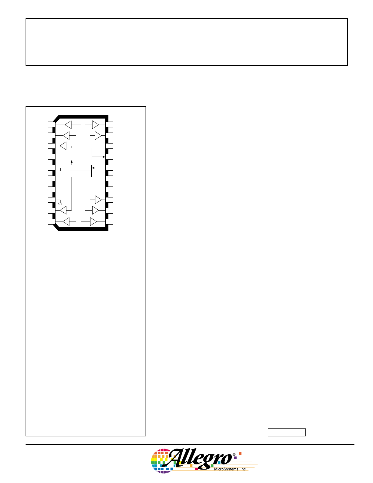
The UCN5910A and UCN5910A-2 are furnished in a 20-pin dual in-line
plastic package. The surface-mount UCN5910LW and UCN5910LW-2 are
furnished in a wide-body, small-outline plastic package (SOIC) with gull-wing
leads. Copper lead frames, reduced supply current requirements, and lower
ABSOLUTE MAXIMUM RATINGS
at T
= 25°C
A
Logic Supply Voltage, VDD................ 15 V
Driver Supply Voltage, V
UCN5910A/LW ......................... 150 V
Suffix “-2” .................................. 140 V
Continuous Output Current Range,
I
....................... -30 mA to +40 mA
OUT
DISCONTINUED PRODUCT
Input Voltage Range,
VIN.................... -0.3 V to VDD + 0.3 V
Package Power Dissipation, PD. See Graph
Operating Temperature Range,
T
............................... -20°C to +85°C
A
—
Storage Temperature Range,
T
.............................. -55°C to +150°C
S
Caution: CMOS devices have input static
BB
FOR REFERENCE ONL
output saturation voltages allow all devices to be operated at ±20 mA from all
outputs (50% duty cycle), at ambient temperatures up to +30°C, or at ±15 mA
to +55°C.
FEATURES
■ High-Speed Source Drivers
■ 140 V (suffix “-2”) or 150 V
Minimum Output Breakdown
■ Improved Replacements
for TL4810B
■ Low Output Saturation Voltages
■ Low-Power CMOS Logic and Latches
■ To 3.3 MHz Data Input Rate
■ Active DMOS Pull-Downs
PRELIMINARY INFORMATION
(Subject to change without notice)
January 18, 2000
protection but are susceptible to damage when
exposed to extremely high static electrical
charges.
Always order by complete part number, e.g., UCN5910A-2 .
Page 2
5910
HIGH-VOLTAGE BiMOS III
10-BIT SERIAL-INPUT,
LATCHED DRIVERS
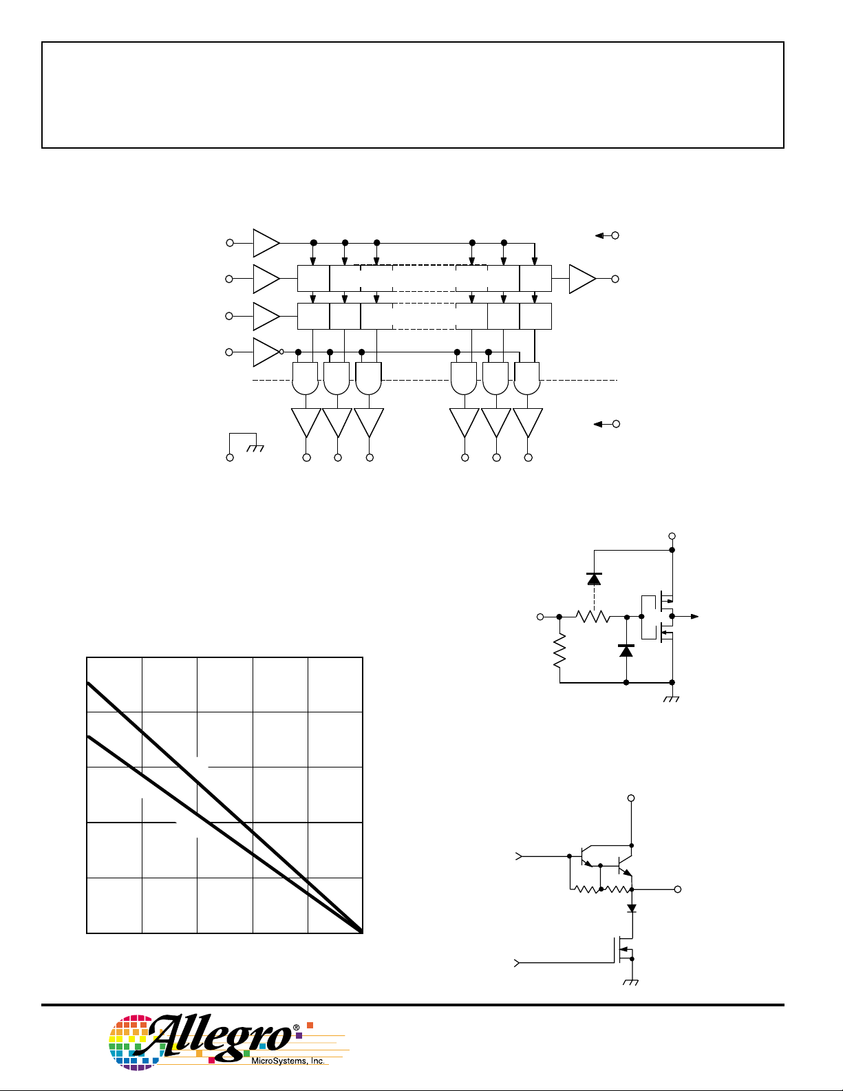
FUNCTIONAL BLOCK DIAGRAM
CLOCK
SERIAL
DATA IN
STROBE
BLANKING
GROUND
OUT1OUT
SERIAL-PARALLEL SHIFT REGISTER
LATCHES
OUT
2
3
LOGIC
SUPPLY
SERIAL
DATA OUT
LOAD
SUPPLY
Dwg. FP-013-1
OUT
N
V
DD
MOS
BIPOLAR
V
BB
TYPICAL INPUT CIRCUIT
V
DD
IN
2.5
2.0
SUFFIX 'A', R = 55
1.5
1.0
S
U
F
F
θJA
=
θJA
°C/W
7
0
°C
/W
IX
'L
W
', R
0.5
0
25
ALLOWABLE PACKAGE POWER DISSIPATION IN WATTS
50 75 100 125 150
AMBIENT TEMPERATURE IN °C
Dwg. GS-004A
TYPICAL OUTPUT DRIVER
115 Northeast Cutoff, Box 15036
Worcester, Massachusetts 01615-0036 (508) 853-5000
Copyright © 1984, 1999, Allegro MicroSystems, Inc.
V
BB
Dwg. EP-010-4A
OUT
N
Dwg. No. A-14,219
Page 3
5910
HIGH-VOLTAGE BiMOS III
10-BIT SERIAL-INPUT,
LATCHED DRIVERS
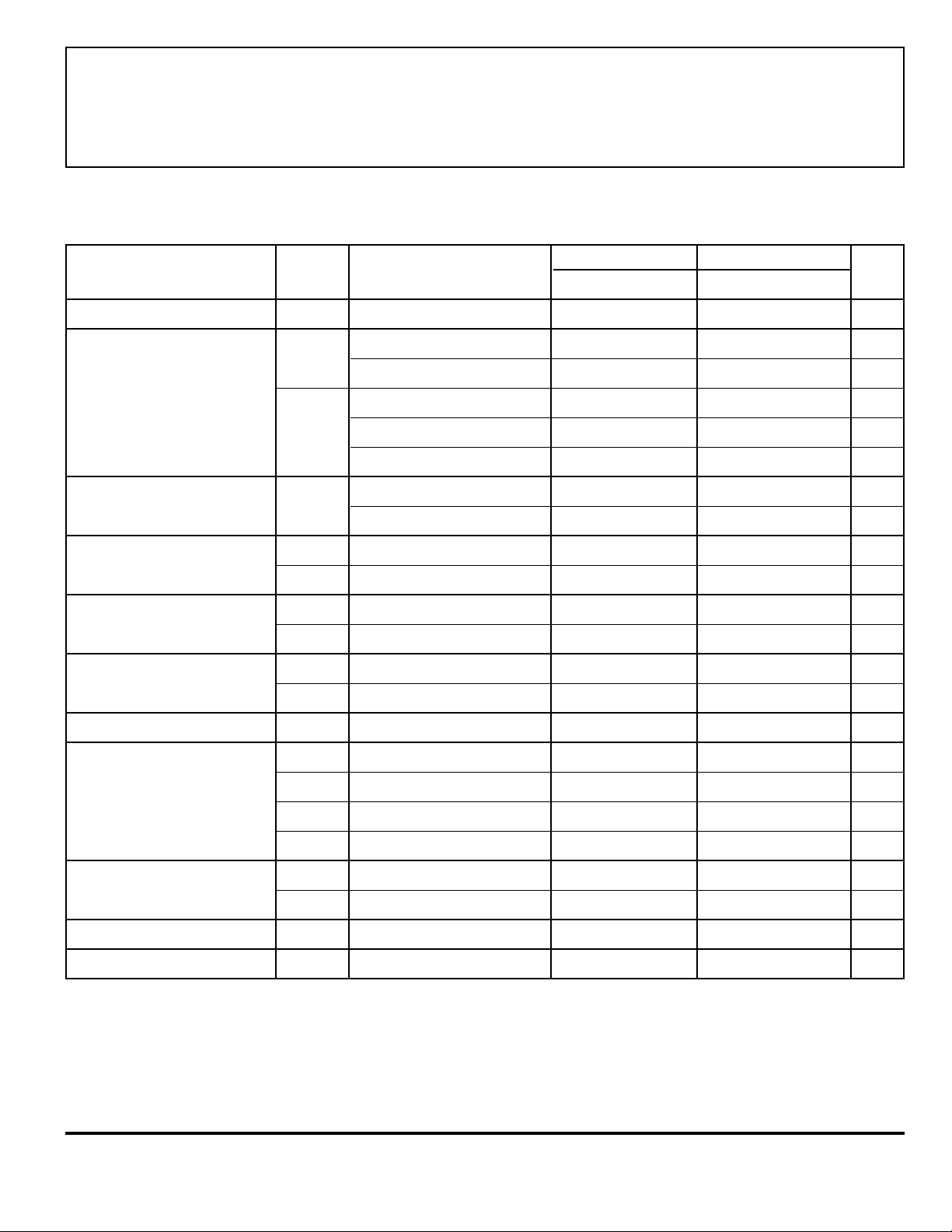
ELECTRICAL CHARACTERISTICS at T
= +25°C, V
A
= 150 V (basic devices) or
BB
140 V (suffix “-2”) unless otherwise noted.
Limits @ VDD = 5 V Limits @ V DD = 12 V
Characteristic Symbol Test Conditions Mln. Typ. Max. Min. Typ. Max. Units
Output Leakage Current I
Output Voltage V
V
Output Pull-Down Current I
Input Voltage V
Input Current I
CEX
OUT(1)
OUT(0)
OUT(0)
IN(1)
V
IN(0)
IN(1)
I
IN(0)
V
= 0 V, T
OUT
Basic, I
OUT
Suffix “-2”, I
I
= 5 mA – 2.5 3.2 – 2.0 3.2 V
OUT
I
= 10 mA – 5.0 – – – – V
OUT
I
= 30 mA – – – – 12 25 V
OUT
V
= 5 V to V
OUT
V
= 20 V to V
OUT
= +70°C – -5.0 -15 – -5.0 -15 µA
A
= -40 mA 145 148 – 145 148 – V
= -40 mA 135 – – 135 – – V
OUT
BB
BB
10 14 – – – – mA
– – – 25 40 – mA
3.5 – 5.3 10.5 – 12.3 V
-0.3 – +0.8 -0.3 – +0.8 V
VIN = V
V
DD
= 0.8 V -0.3 – -0.8 -0.3 – -0.8 µA
IN
–0.050.5 –0.051.0 µA
Serial Data Output Voltage V
OUT(1)
V
OUT(0)
Maximum Clock Frequency f
Supply Current I
DD(1)
I
DD(0)
I
I
Blanking to Output Delay t
t
Output Fall Time t
Output Rise Time t
clk
BB(1)
BB(0)
PHL
PLH
f
r
I
= -200 µA 4.5 5.0 – 11.7 12 – V
OUT
I
= 200 µA – 200 250 – 200 250 mV
OUT
3.3 5.0 – 5.0 – – MHz
All Outputs High – 320 450 – 650 800 µA
All Outputs Low – 320 450 – 650 800 µA
Outputs High, No Load – 0.6 1.75 – 0.9 1.75 mA
Outputs Low – 10 100 – 10 100 µA
C
= 30 pF, 50% to 50% – 0.7 0.9 – 0.35 0.6 µs
L
C
= 30 pF, 50% to 50% – 0.9 1.3 – 0.35 0.6 µs
L
C
= 30 pF, 90% to 10% – 1.3 1.5 – 0.6 0.7 µs
L
C
= 30 pF, 10% to 90% – 1.2 1.5 – 1.0 1.2 µs
L
Negative current is defined as coming out of (sourcing) the specified device terminal.
Page 4

5910
HIGH-VOLTAGE BiMOS III
10-BIT SERIAL-INPUT,
LATCHED DRIVERS
CLOCK
DATA IN
STROBE
BLANKING
OUT
A D
B
E F
C
G
N
Dwg. No. A-12,649A
TIMING CONDITIONS
(T
= +25°C, V
A
A. Minimum Data Active Time Before Clock Pulse
(Data Set-Up Time) ........................................................................... 75 ns
B. Minimum Data Active Time After Clock Pulse
(Data Hold Time) ............................................................................... 75 ns
C. Minimum Data Pulse Width ............................................................. 150 ns
D. Minimum Clock Pulse Width ........................................................... 100 ns
E. Minimum Time Between Clock Activation and Strobe .................... 300 ns
F. Minimum Strobe Pulse Width .......................................................... 100 ns
G. Typical Time Between Strobe Activation and
Output Transition ............................................................................. 750 ns
= 12 V, Logic Levels are VDD and Ground)
DD
Serial Data present at the input is transferred
to the shift register on the logic “0” to logic “1”
transition of the CLOCK input pulse. On
succeeding CLOCK pulses, the registers shift data
information towards the SERIAL DATA OUTPUT. The SERIAL DATA must appear at the
input prior to the rising edge of the CLOCK input
waveform.
Information present at any register is transferred to the respective latch when the STROBE
is high (serial-to-parallel conversion). The
latches will continue to accept new data as long as
the STROBE is held high. Applications where
the latches are bypassed (STROBE tied high) will
require that the BLANKING input be high during
serial data entry.
When the BLANKING input is high, the
output source drivers are disabled (OFF); the
DMOS sink drivers are ON. The information
stored in the latches is not affected by the
BLANKING input. With the BLANKING input
low, the outputs are controlled by the state of
their respective latches.
TRUTH TABLE
Serial Shift Register Contents Serial Latch Contents Output Contents
Data Clock Data Strobe
Input Input I
HHR
LLR
XR
L = Low Logic Level H = High Logic Level X = Irrelevant P = Present State R = Previous State
1I2I3
1R2R3
XXX...X X X L R1R2R3... R
P1P2P3... P
1R2
1R2
... I
... R
... R
... R
N-1IN
N-2RN-1
N-2RN-1
N-1RN
N-1PN
Output Input I1I2I3... I
R
N-1
R
N-1
R
N
P
N
HP1P2P3... P
X X X ... X X H L L L ... L L
115 Northeast Cutoff, Box 15036
Worcester, Massachusetts 01615-0036 (508) 853-5000
N-1IN
N-1 RN
N-1 PN
Blanking I1I2I3... I
LP1P2P3... P
I
N-1
N-1 PN
N
Page 5

0.280
0.240
20
HIGH-VOLTAGE BiMOS III
UCN5910A & UCN5910A-2
Dimensions in Inches
(controlling dimensions)
11
5910
10-BIT SERIAL-INPUT,
LATCHED DRIVERS
0.014
0.008
0.430
MAX
0.300
BSC
0.210
MAX
7.11
6.10
0.015
MIN
20
1
0.070
0.045
0.022
0.014
1.060
0.980
0.100
BSC
10
0.005
MIN
0.150
0.115
Dwg. MA-001-20 in
Dimensions in Millimeters
(for reference only)
0.355
11
1
1.77
1.15
26.92
24.89
2.54
BSC
10
0.13
MIN
0.204
7.62
BSC
10.92
MAX
5.33
MAX
0.39
MIN
0.558
0.356
3.81
2.93
NOTES:1. Exact body and lead configuration at vendor’s option within limits shown.
2. Lead spacing tolerance is non-cumulative.
3. Lead thickness is measured at seating plane or below.
Dwg. MA-001-20 mm
Page 6

5910
HIGH-VOLTAGE BiMOS III
10-BIT SERIAL-INPUT,
LATCHED DRIVERS
UCN5910LW & UCN5910LW-2
20 11
Dimensions in Inches
(for reference only)
0.0125
0.0091
0.2992
0.2914
0.020
0.013
0.0926
0.1043
7.60
7.40
1 2
0.0040
20
MIN.
3
0.5118
0.4961
Dimensions in Millimeters
(controlling dimensions)
11
0.050
BSC
0.419
0.394
10.65
10.00
0° TO 8°
0.050
0.016
Dwg. MA-008-20 in
0.32
0.23
0.51
0.33
2.65
2.35
1
0.10
2
MIN.
3
13.00
12.60
1.27
BSC
NOTES:1. Exact body and lead configuration at vendor’s option within limits shown.
2. Lead spacing tolerance is non-cumulative.
115 Northeast Cutoff, Box 15036
Worcester, Massachusetts 01615-0036 (508) 853-5000
0° TO 8°
Dwg. MA-008-20 mm
1.27
0.40
Page 7

HIGH-VOLTAGE BiMOS III
This page intentionally left blank
5910
10-BIT SERIAL-INPUT,
LATCHED DRIVERS
Page 8

5910
HIGH-VOLTAGE BiMOS III
10-BIT SERIAL-INPUT,
LATCHED DRIVERS
BiMOS II (Series 5800), BiMOS III (Series 5900),
& DABiC IV (Series 6800) INTELLIGENT POWER
INTERFACE DRIVERS
Function Output Ratings* Part Number
SERIAL-INPUT LATCHED DRIVERS
8-Bit (saturated drivers) -120 mA 50 V‡ 5895
8-Bit 350 mA 50 V 5821
8-Bit 350 mA 80 V 5822
8-Bit 350 mA 50 V‡ 5841
8-Bit 350 mA 80 V‡ 5842
8-Bit (constant-current LED driver) 75 mA 17 V 6275
9-Bit 1.6 A 50 V 5829
10-Bit (active pull-downs) -25 mA 60 V 5810-F and 6809/10
10-Bit (active pull-downs) -40 mA 140 V 5910-2
10-Bit (active pull-downs) -40 mA 150 V 5910
12-Bit (active pull-downs) -25 mA 60 V 5811 and 6811
16-Bit (constant-current LED driver) 75 mA 17 V 6276
20-Bit (active pull-downs) -25 mA 60 V 5812-F and 6812
32-Bit (active pull-downs) -25 mA 60 V 5818-F and 6818
32-Bit 100 mA 30 V 5833
32-Bit (saturated drivers) 100 mA 40 V 5832
PARALLEL-INPUT LATCHED DRIVERS
4-Bit 350 mA 50 V‡ 5800
†
8-Bit -25 mA 60 V 5815
8-Bit 350 mA 50 V‡ 5801
SPECIAL-PURPOSE DEVICES
Unipolar Stepper Motor Translator/Driver 1.25 A 50 V‡ 5804
Addressable 28-Line Decoder/Driver 450 mA 30 V 6817
* Current is maximum specified test condition, voltage is maximum rating. See specification for sustaining voltage limits.
Negative current is defined as coming out of (sourcing) the output.
† Complete part number includes additional characters to indicate operating temperature range and package style.
‡ Internal transient-suppression diodes included for inductive-load protection.
Allegro MicroSystems, Inc. reserves the right to make, from time to time, such
departures from the detail specifications as may be required to permit improvements in
the design of its products.
The information included herein is believed to be accurate and reliable. However,
Allegro MicroSystems, Inc. assumes no responsibility for its use; nor for any infringements of patents or other rights of third parties which may result from its use.
115 Northeast Cutoff, Box 15036
Worcester, Massachusetts 01615-0036 (508) 853-5000
 Loading...