

Page 1
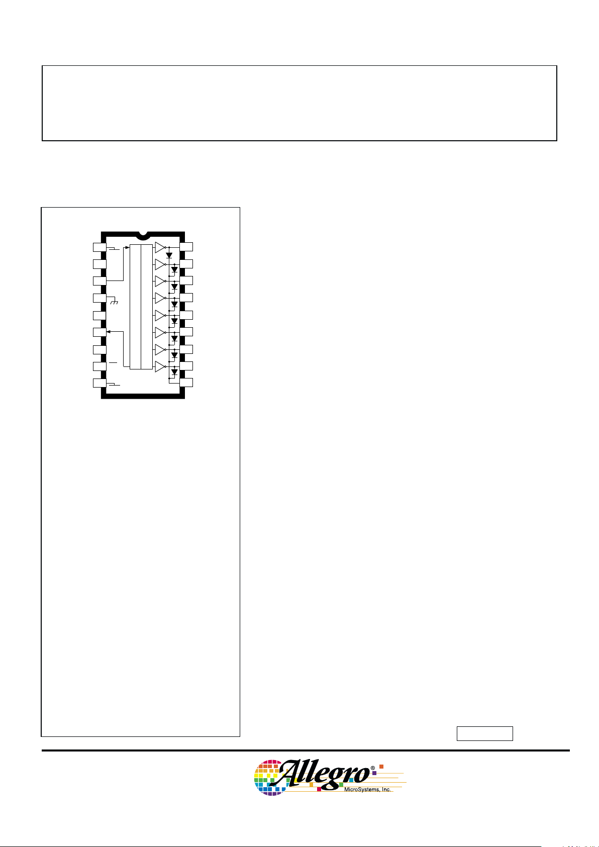
The merging of low-power CMOS logic and bipolar output power
drivers permit the UCN5841/42A, UCN5841/42LW, and A5841/42SLW
integrated circuits to be used in a wide variety of peripheral power
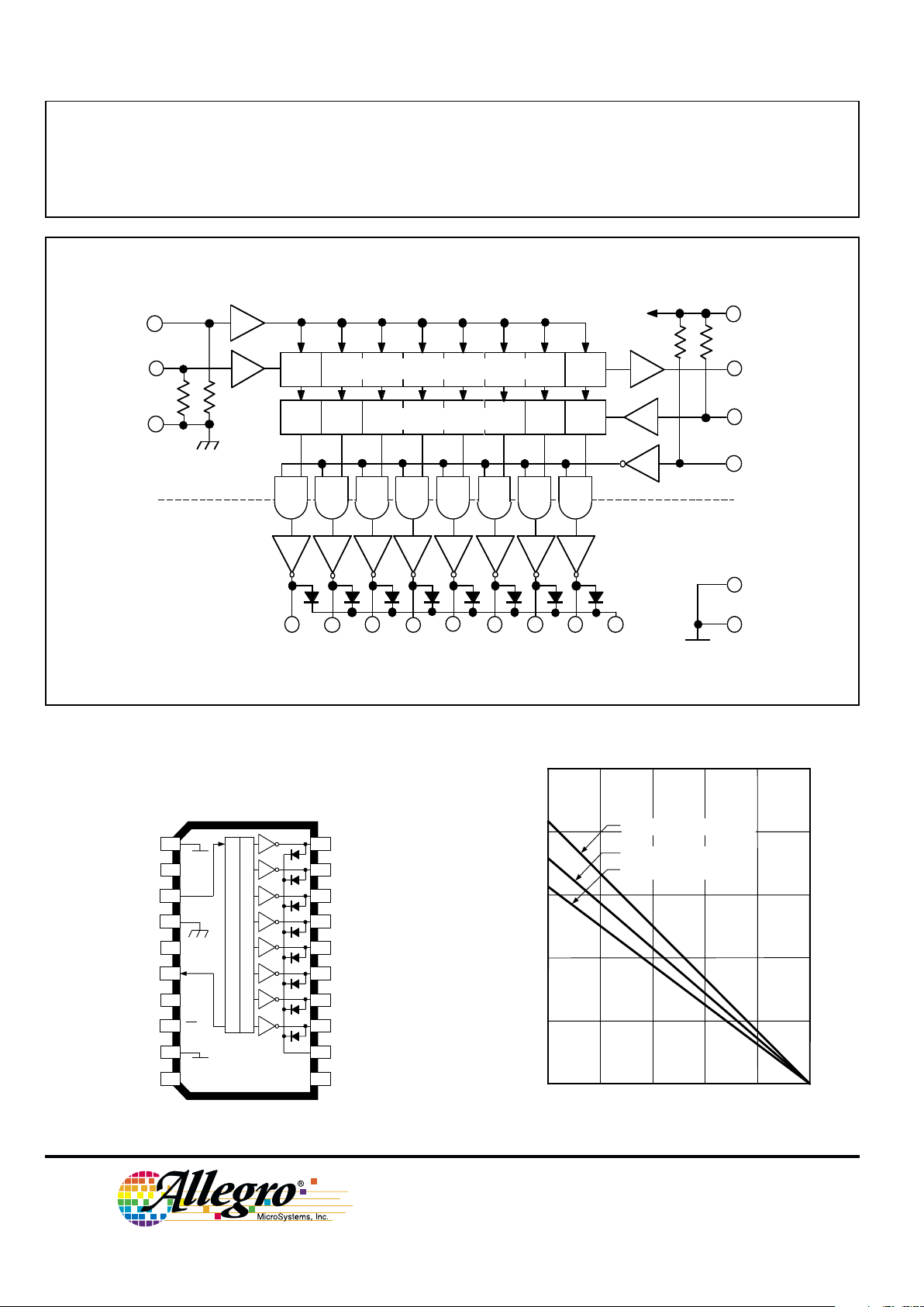
driver applications. Each device has an eight-bit CMOS shift register
and CMOS control circuitry, eight CMOS data latches, and eight bipolar
current-sinking Darlington output drivers. The 500 mA npn Darlington
outputs, with integral transient-suppression diodes, are suitable for use
with relays, solenoids, and other inductive loads. Except for packaging
and the maximum driver output voltage ratings, the UCN5841A,
UCN5841LW, A5841SLW, UCN5842A, UCN5842LW, and A5842SLW
are identical. All package variations of the 5842 offer premium performance with a minimum output-breakdown voltage rating of 80 V (50 V
sustaining). All drivers can be operated with a split supply where the
negative supply is up to -20 V.
BiMOS II devices have higher data-input rates than the earlier
BiMOS circuits. With a 5 V logic supply, they will typically operate at
better than 5 MHz. With a 12 V supply, significantly higher speeds are
obtained. The CMOS inputs are compatible with standard CMOS and
NMOS logic levels. TTL circuits may require the use of appropriate
pull-up resistors. By using the serial data output, drivers can be
cascaded for interface applications requiring additional drive lines.
The UCN584xA devices are furnished in a standard 18-pin plastic
DIP; the UCN584xLW devices are in an 18-lead surface-mountable
wide-body SOIC package; the A584xSLW devices are provided in a 20lead wide-body SOIC package with improved thermal characteristics.
The A5841SLW and UCN5841LW drivers are also available for
operation to a temperature of -40°C. To order, change the suffix from
‘SLW’ to ‘ELW’, or change the prefix from ‘UCN’ to ‘UCQ’.
FEATURES
■ To 3.3 MHz Data-Input Rate
■ CMOS, NMOS, TTL Compatible Inputs
■ Internal Pull-Up/Pull-Down Resistors
■ Low-Power CMOS Logic and Latches,
■ High-Voltage Current-Sink Outputs
■ Output Transient-Protection Diodes
■ Single or Split Supply Operation
■ DIP or SOIC Packaging
■ Automotive Capable
BiMOS II 8-BIT SERIAL-INPUT,
LATCHED DRIVERS
Always order by complete part number, e.g., A5841SLW .
Data Sheet
26185.14F
5841
AND
5842
SUB
V
EE
2
3
4
5
6
7
8
SERIAL
DATA OUT
SERIAL
DATA IN
OUTPUT
ENABLE
LOGIC
SUPPLY
STROBE
LOGIC
GROUND
CLOCK CLK
V
DD
ST
OE
1
SHIFT REGISTER
LATCHES
12
13
14
15
16
17
18 OUT
1
OUT
2
OUT
3
OUT
8
OUT
7
OUT
6
OUT
5
OUT
4
9
SUB
10
11
Dwg. PP-026-1
K
V
EE
UCN5841A & UCN5842A
Note that the UCN584xA (dual in-line package) and
UCN584xLW (small-outline IC package) are electrically
identical and share a common terminal number assignment.
ABSOLUTE MAXIMUM RATINGS
at 25°C Free-Air Temperature
Output Voltage, V
CE
(5841). . . . . . . . . . . . . . . . . . . . . . 50 V
(5842). . . . . . . . . . . . . . . . . . . . . . 80 V
Output Voltage, V
CE(sus)
(5841). . . . . . . . . . . . . . . . . . . . . 35 V†
(5842). . . . . . . . . . . . . . . . . . . . . 50 V†
Logic Supply Voltage Range,
V
DD
. . . . . . . . . . . . . . . . 4.5 V to 15 V
V
DD
with Reference to VEE. . . . . 25 V
Emitter Supply Voltage, V
EE
. . . . . . . -20 V
Input Voltage Range,
VIN. . . . . . . . . . . -0.3 V to VDD + 0.3 V
Continuous Output Current,
I
OUT
. . . . . . . . . . . . . . . . . . . . 500 mA
Package Power Dissipation,
P
D
. . . . . . . . . . . . . . . . . . . See Graph
Operating Temperature Range,
TA. . . . . . . . . . . . . . . . -20°C to +85°C
Storage Temperature Range,
TS. . . . . . . . . . . . . . . -55°C to +150°C
†For inductive load applications.
Caution: CMOS devices have input static protection
but are susceptible to damage when exposed to
extremely high static electrical charges.
Page 2
5841
AND
5842
8-BIT SERIAL-INPUT,
LATCHED DRIVERS
115 Northeast Cutoff, Box 15036
Worcester, Massachusetts 01615-0036 (508) 853-5000
Copyright © 1985, 2000 Allegro MicroSystems, Inc.
FUNCTIONAL BLOCK DIAGRAM
(‘A’ Package Shown)
MOS
BIPOLAR
OUT1OUT
2
LOGIC
GROUND
STROBE
OUTPUT ENABLE
(ACTIVE LOW)
SERIAL
DATA OUT
6
8
7
Dwg. FP-013-2
9
POWER
GROUND
SUB
OUT
3
CLOCK
SERIAL
DATA IN
SERIAL-PARALLEL SHIFT REGISTER
LATCHES
V
DD
LOGIC
SUPPLY
2
3
4
18
OUT6OUT7OUT
8
17 16 13 12 11
OUT4OUT
5
15
14
5
K
10
1
50 75 100 125 150
2.5
0.5
0
ALLOWABLE PACKAGE POWER DISSIPATION IN WATTS
AMBIENT TEMPERATURE IN °C
2.0
1.5
1.0
25
Dwg. GP-022-4
18-LEAD SOIC, R
θJA
= 80°C/W
20-LEAD SOIC, R
θJA
= 70°C/W
18-PIN DIP, R
θJA
= 60°C/W
SERIAL
DATA OUT
POWER
GROUND
SERIAL
DATA IN
OUTPUT
ENABLE
OUT
1
OUT
2
OUT
3
NO
CONNECT.
NO
CONNECT.
NC
NC
LOGIC SUPPLY
STROBE
GROUND
CLOCK
OUT
6
OUT
7
OUT
8
OUT
5
OUT
4
Dwg. PP-029-3
13
14
15
16
17
19
12
18
20
11
1
2
3
8
9
4
5
6
7
10
SUB
CLK
SUB
V
DD
ST
OE
POWER
GROUND
K
LATCHES
SHIFT REGISTER
A5841SLW
& A5842SLW
Page 3
5841
AND
5842
8-BIT SERIAL-INPUT,
LATCHED DRIVERS
www.allegromicro.com
ELECTRICAL CHARACTERISTICS at TA = +25°C, VDD = 5 V, VEE = 0 V
(unless otherwise specified).
Applicable Limits
Characteristic Symbol Devices Test Conditions Min. Max. Unit
Output Leakage Current I
CEX
5841* V
OUT
= 50 V — 50 µA
V
OUT
= 50 V, TA = +70°C — 100 µA
5842* V
OUT
= 80 V — 50 µA
V
OUT
= 80 V, TA = +70°C — 100 µA
Collector-Emitter V
CE(SAT)
All I
OUT
= 100 mA — 1.1 V
I
OUT
= 200 mA — 1.3 V
I
OUT
= 350 mA, VDD = 7.0 V — 1.6 V
Collector-Emitter V
CE(sus)
5841* I
OUT
= 350 mA, L = 2 mH 35 — V
5842* I
OUT
= 350 mA, L = 2 mH 50 — V
Input Voltage V
IN(0)
All — 0.8 V
V
IN(1)
All VDD = 12 V 10.5 — V
V
DD
= 10 V 8.5 — V
V
DD
= 5.0 V 3.5 — V
Input Resistance R
IN
All VDD = 12 V 50 — kΩ
V
DD
= 10 V 50 — kΩ
V
DD
= 5.0 V 50 — kΩ
Supply Current I
DD(ON)
All All Drivers ON, VDD = 12 V — 16 mA
All Drivers ON, V
DD
= 10 V — 14 mA
All Drivers ON, V
DD
= 5.0 V — 8.0 mA
I
DD(OFF)
All All Drivers OFF, VDD = 12 V — 2.9 mA
All Drivers OFF, V
DD
= 10 V — 2.5 mA
All Drivers OFF, V
DD
= 5.0 V — 1.6 mA
Clamp Diode I
R
5841* VR = 50 V — 50 µA
5842* V
R
= 80 V — 50 µA
Clamp Diode V
F
All IF = 350 mA — 2.0 V
Saturation Voltage
Sustaining Voltage
Leakage Current
Forward Voltage
* Complete part number includes a prefix (A or UCN) and a suffix (A, LW, or SLW) as follows:
UCN5841A, UCN5841LW, or A5841SLW,
UCN5842A, UCN5842LW, or A5842SLW.
Page 4

5841
AND
5842
8-BIT SERIAL-INPUT,
LATCHED DRIVERS
115 Northeast Cutoff, Box 15036
Worcester, Massachusetts 01615-0036 (508) 853-5000
TYPICAL INPUT CIRCUITS
Dwg. EP-010-3
TIMING CONDITIONS
(TA = +25°C, VDD = 5.0 V, Logic Levels are VDD and Ground)
A. Minimum Data Active Time Before Clock Pulse
(Data Set-Up Time) . . . . . . . . . . . . . . . . . . . . . . . . . . . . . . . . . . . . . 75 ns
B. Minimum Data Active Time After Clock Pulse
(Data Hold Time) . . . . . . . . . . . . . . . . . . . . . . . . . . . . . . . . . . . . . . . 75 ns
C. Minimum Data Pulse Width . . . . . . . . . . . . . . . . . . . . . . . . . . . . . . . . . 150 ns
D. Minimum Clock Pulse Width . . . . . . . . . . . . . . . . . . . . . . . . . . . . . . . . 150 ns
E. Minimum Time Between Clock Activation and Strobe . . . . . . . . . . . . 300 ns
F. Minimum Strobe Pulse Width . . . . . . . . . . . . . . . . . . . . . . . . . . . . . . . 100 ns
G. Typical Time Between Strobe Activation and
Output Transition . . . . . . . . . . . . . . . . . . . . . . . . . . . . . . . . . . . . . 1.0
µs
Serial Data present at the input is transferred to the shift register
on the logic “0” to logic “1” transition of the CLOCK input pulse. On
succeeding CLOCK pulses, the registers shift data information towards
the SERIAL DATA OUTPUT. The SERIAL DATA must appear at the
input prior to the rising edge of the CLOCK input waveform.
Information present at any register is transferred to its respective
latch when the STROBE is high (serial-to-parallel conversion). The
latches will continue to accept new data as long as the STROBE is held
high. Applications where the latches are bypassed (STROBE tied high)
will require that the ENABLE input be high during serial data entry.
When the ENABLE input is high, all of the output buffers are
disabled (OFF) without affecting the information stored in the latches or
shift register. With the ENABLE input low, the outputs are controlled by
the state of the latches.
IN
V
DD
A
D
B
C
E
F
CLOCK
DATA IN
STROBE
OUTPUT
ENABLE
OUT
N
G
Dwg. No. A-12,627
TYPICAL OUTPUT DRIVER
V
DD
Dwg. EP-010-4A
CLOCK
SERIAL
DATA IN
Dwg. EP-021-8
OUT
K
V
EE
SUB
STROBE
OUTPUT
ENABLE
Page 5
5841
AND
5842
8-BIT SERIAL-INPUT,
LATCHED DRIVERS
www.allegromicro.com
TRUTH TABLE
Serial Shift Register Contents Serial Latch Contents Output Contents
Data Clock Data Strobe Output
Input Input I
1I2I3
.............. I
8
Output Input I1I2I3.............. I8Enable I1I2I3.............. I
8
HHR
1R2
.............. R
7
R
7
LLR
1R2
.............. R
7
R
7
XR
1R2R3
.............. R
8
R
8
X X X .............. X X L R1R2R3.............. R
8
P1P2P3.............. P
8
P
8
HP1P2P3.............. P
8
LP1P2P3.............. P
8
X X X .............. X H H H H .............. H
L = Low Logic Level H = High Logic Level X = Irrelevant P = Present State R = Previous State
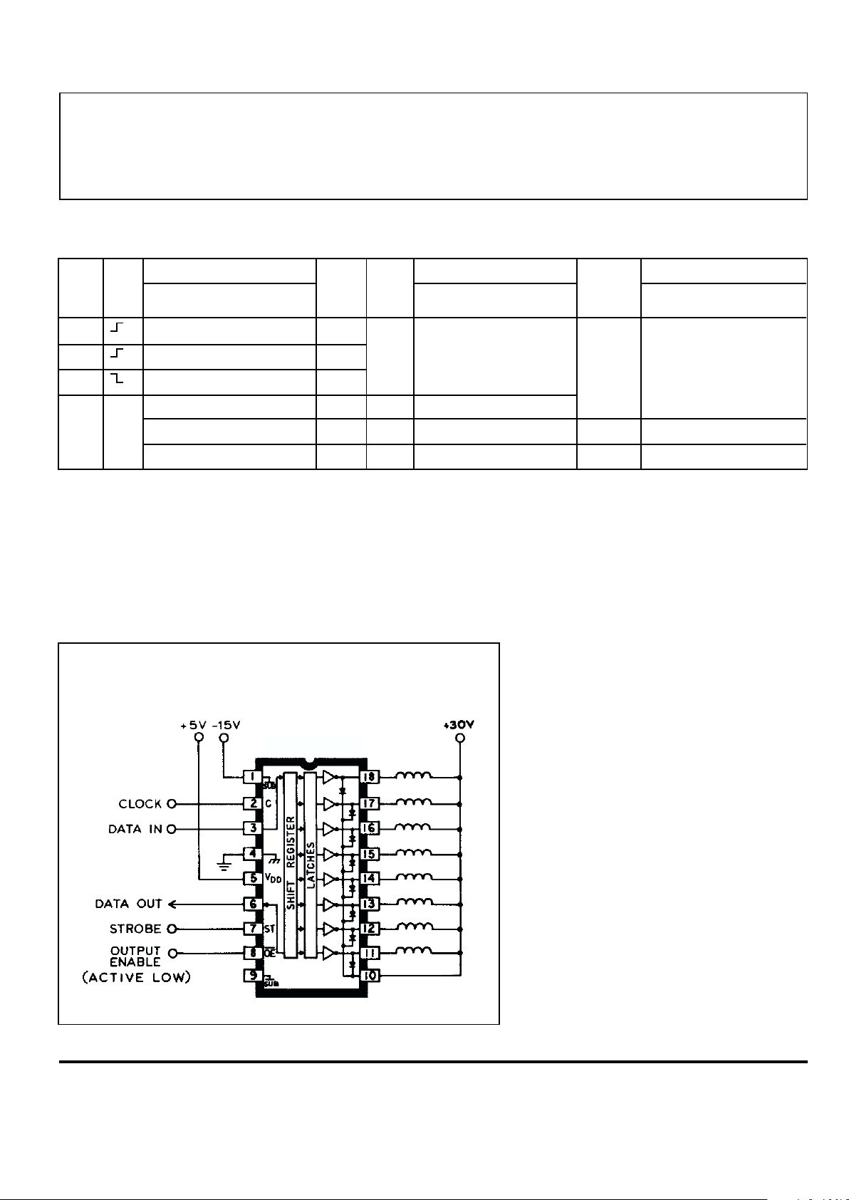
TYPICAL APPLICATION
RELAY/SOLENOID DRIVER
Using Split Supply
Dwg. No. A-12,547
UCN5842A
The products described here are manufactured
under one or more U.S. patents or U.S. patents
pending.
Allegro MicroSystems, Inc. reserves the right to
make, from time to time, such departures from the detail
specifications as may be required to permit improvements in the performance, reliability, or
manufacturability of its products. Before placing an
order, the user is cautioned to verify that the information being relied upon is current.
Allegro products are not authorized for use as
critical components in life-support devices or systems
without express written approval.
The information included herein is believed to be
accurate and reliable. However, Allegro
MicroSystems, Inc. assumes no responsibility for its
use; nor for any infringement of patents or other rights
of third parties which may result from its use.
Page 6

5841
AND
5842
8-BIT SERIAL-INPUT,
LATCHED DRIVERS
115 Northeast Cutoff, Box 15036
Worcester, Massachusetts 01615-0036 (508) 853-5000
0.355
0.204
7.62
BSC
Dwg. MA-001-18A mm
10.92
MAX
18
1
9
7.11
6.10
5.33
MAX
1.77
1.15
0.39
MIN
0.558
0.356
2.54
BSC
0.13
MIN
3.81
2.93
10
23.37
22.35
UCN5841A and UCN5842A
Dimensions in Inches
(controlling dimensions)
Dimensions in Millimeters
(for reference only)
NOTES: 1. Exact body and lead configuration at vendor’s option within limits shown.
2. Lead spacing tolerance is non-cumulative.
3. Lead thickness is measured at seating plane or below.
0.014
0.008
0.300
BSC
Dwg. MA-001-18A in
0.430
MAX
18
1
9
0.280
0.240
0.210
MAX
0.070
0.045
0.015
MIN
0.022
0.014
0.100
BSC
0.005
MIN
0.150
0.115
10
0.920
0.880
Page 7

5841
AND
5842
8-BIT SERIAL-INPUT,
LATCHED DRIVERS
www.allegromicro.com
UCN5841LW and UCN5842LW
Dimensions in Inches
(for reference only)
Dimensions in Millimeters
(controlling dimensions)
NOTES: 1. Exact body and lead configuration at vendor’s option within limits shown.
2. Lead spacing tolerance is non-cumulative.
0° TO 8°
1 2
3
0.020
0.013
0.0040
MIN.
0.0125
0.0091
0.050
0.016
D
wg. MA-008-18A in
0.050
BSC
18 10
0.419
0.394
0.2992
0.2914
0.4625
0.4469
0.0926
0.1043
0° TO 8°
1
18
2
3
0.51
0.33
0.10
MIN.
0.32
0.23
1.27
0.40
Dwg. MA-008-18A mm
1.27
BSC
10
7.60
7.40
10.65
10.00
11.75
11.35
2.65
2.35
Page 8

5841
AND
5842
8-BIT SERIAL-INPUT,
LATCHED DRIVERS
115 Northeast Cutoff, Box 15036
Worcester, Massachusetts 01615-0036 (508) 853-5000
0° TO 8°
1 2
3
0.020
0.013
0.0040
MIN.
0.0125
0.0091
0.050
0.016
Dwg. MA-008-20 in
0.050
BSC
20 11
0.2992
0.2914
0.419
0.394
0.5118
0.4961
0.0926
0.1043
0° TO 8°
1
20
2
3
0.51
0.33
0.10
MIN.
Dwg. MA-008-20 mm
1.27
BSC
11
0.32
0.23
1.27
0.40
7.60
7.40
10.65
10.00
13.00
12.60
2.65
2.35
A5841SLW and A5842SLW
Dimensions in Inches
(for reference only)
Dimensions in Millimeters
(controlling dimensions)
NOTES: 1. Exact body and lead configuration at vendor’s option within limits shown.
2. Lead spacing tolerance is non-cumulative.
 Loading...