

Page 1

1. Description
2. Features
UCB1510
AC97 digital modem codec
Rev. 01 — 4 February 2000 Preliminary specification
The UCB1510 is a single chip, integrated mixed signal telecom codec that can
directly be connected to a DAA and supports high speed modem protocols. The
general purpose I/O pins provide programmable inputs and/or outputs to the system.
The UCB1510 has a serial AClink interface intended to communicate to the system
controller. Both the codec input data and codec output data and the control register
data are multiplexed on this interface.
c
c
3. Applications
■ Sigma delta telecom codec with programmable sample rate, including digitally
controlled input voltage level, mute, loop back and clip detection functions. The
telecom codec can be directly connected to a Data Access Arrangement (DAA)
and includes a built in sidetone suppression circuit
■ AClink (rev 2.1) interface with secondary codec support
■ 3.3 V supply voltageand built in power saving modes make the UCB1510 optimal
for portable and battery powered applications
■ 5 V tolerant interface for motherboard/PC add on
■ Maximum operating current 25 mA
■ 8 general purpose IO pins for line interface control
■ Interrupt detection driven wake up sequence for ring detect
■ Low cost 12.288 MHz crystal
■ Standalone modems
■ Integrated modems
■ Audio/Modem Riser (AMR) Cards
■ Mobile Daughter Cards (MDC)
Page 2
Philips Semiconductors
UCB1510
AC97 digital modem codec
4. Ordering information
Table 1: Ordering information
Type number Package
Name Description Version
UCB1510DB SSOP28 plastic shrink small outline package, 28 leads, body width 5.3mm SOT341-1
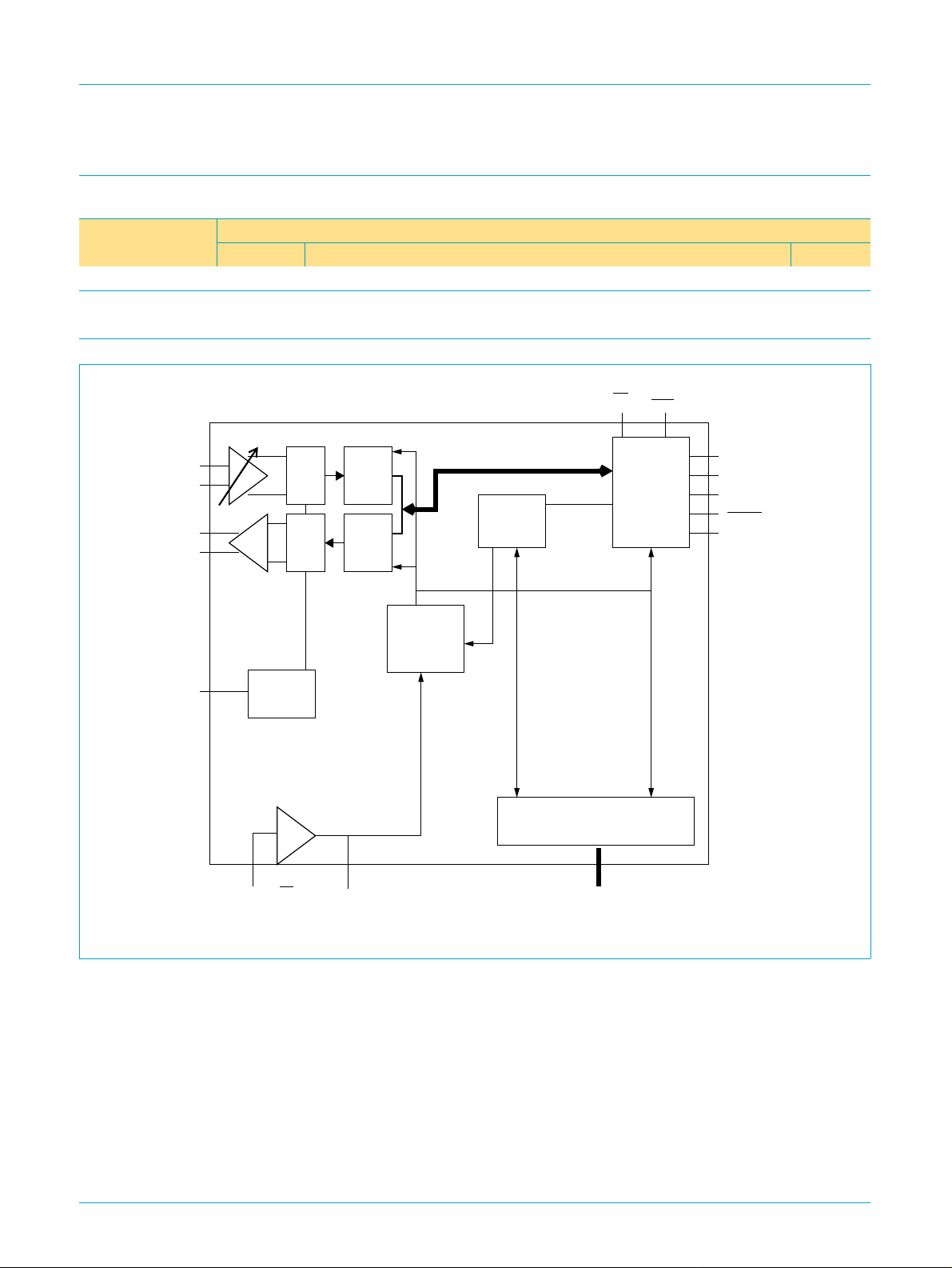
5. Block diagram
A0
PON
TINP
TINN
TOUTP
TOUTN
VREFBYP
Voltage
reference
XTAL_IN/A1
ADC
DAC
down
sample
filter
up
sample
filter
XTAL_OUT
Clock buffers &
sample rate
dividers
Line1 PCM flow
data /
control
registers
GPIO
IO[7:0]
Serial bus
interface
SDOUT
SDIN
SYNC
RESET
BIT_CLK
Fig 1. Block diagram
9397 750 06856
Preliminary specification Rev. 01 — 4 February 2000 2 of 32
© Philips Electronics N.V. 2000. All rights reserved.
Page 3

Philips Semiconductors
6. Pinning information
6.1 Pinning
UCB1510
AC97 digital modem codec
VDDD
IO0
IO1
IO2
IO3
RESET
PON
SYNC
SDOUT
VSSD
SDIN
BIT_CLK
VDDD
Fig 2. Pin configuration
6.2 Pin description
1
2
3
4
5
6
7
A0
8
9
10
11
12
13
14 15
UCB1510
28
XTAL_OUT
27
XTAL_IN/A1
26
VSSA
25
TINN
24
TINP
23
VREFBYP
22
TOUTN
21
TOUTP
20
VDDA
19
VSSD
18
IO7
17
IO6
16
IO5
IO4
Table 2: Pin description
Symbol Pin Reset
state
V
DDD
1 - S digital supply
[1]
Type
IO0 2 input I/O
IO1 3 input I/O
IO2 4 input I/O
IO3 5 input I/O
RESET 6 - I
A0 7 - I
PON 8 - I
SYNC 9 - I/O
SDOUT 10 - I
V
SSD
SDIN 12 0
BIT_CLK 13 V
DDD
11 - S digital ground
[4]
[3]
O
I/O
14 - S digital supply
IO4 15 input I/O
[2]
Description
C
C
C
C
C
C
general purpose I/O pins
general purpose I/O pins
general purpose I/O pins
general purpose I/O pins
asynchronous reset input
address select (for secondary codec) -
inverted polarity
C
C
C
C
C
C
asynchronous cold reset
AClink synchronization input
AClink data input
AClink data output
AClink serial interface clock
general purpose I/O pins
9397 750 06856
Preliminary specification Rev. 01 — 4 February 2000 3 of 32
© Philips Electronics N.V. 2000. All rights reserved.
Page 4

Philips Semiconductors
UCB1510
AC97 digital modem codec
Table 2: Pin description
Symbol Pin Reset
IO5 16 input I/O
IO6 17 input I/O
IO7 18 input I/O
V
SSD
V
DDA
19 - S digital ground
20 - S analog supply
TOUTP 21 hi Z O
TOUTN 22 hi Z O
VREFBYP 23 hi Z I/O
TINP 24 - I
TINN 25 - I
V
SSA
XTAL_IN/
26 - S analog ground
A1 27 -
…continued
[1]
state
[3]
Type
C
C
C
A
A
A
A
A
IA/I
C
[2]
Description
general purpose I/O pins
general purpose I/O pins
general purpose I/O pins
positive telecom codec output
negative telecom codec output
external reference voltage bypass
positive telecom codec input
negative telecom codec input
Xtal oscillator/master clock input or inverted
secondary address
XTAL_OUT 28 -
[1] After cold or warm reset, the AClink interface is active with MLNK bit reset.
[2] I/OC = CMOS bidirectional; ID = digital input; S = supply; OA = analog output; IC = CMOS input;
IA= analog input; I/OA = analog bidirectional; OC = CMOS output.
[3] BIT_CLK is an input for AClink secondary codec, an output for primary codec. When BIT_CLK is an
output, the XTAL oscillator is active.
[4] SDIN is driving a 0 until a valid SYNC framing signal is received after cold reset.
[3]
O
A
Xtal oscillator output
9397 750 06856
Preliminary specification Rev. 01 — 4 February 2000 4 of 32
© Philips Electronics N.V. 2000. All rights reserved.
Page 5
Philips Semiconductors
7. Functional description
The functional description of the devices id described in Section 8 through
Section 15.
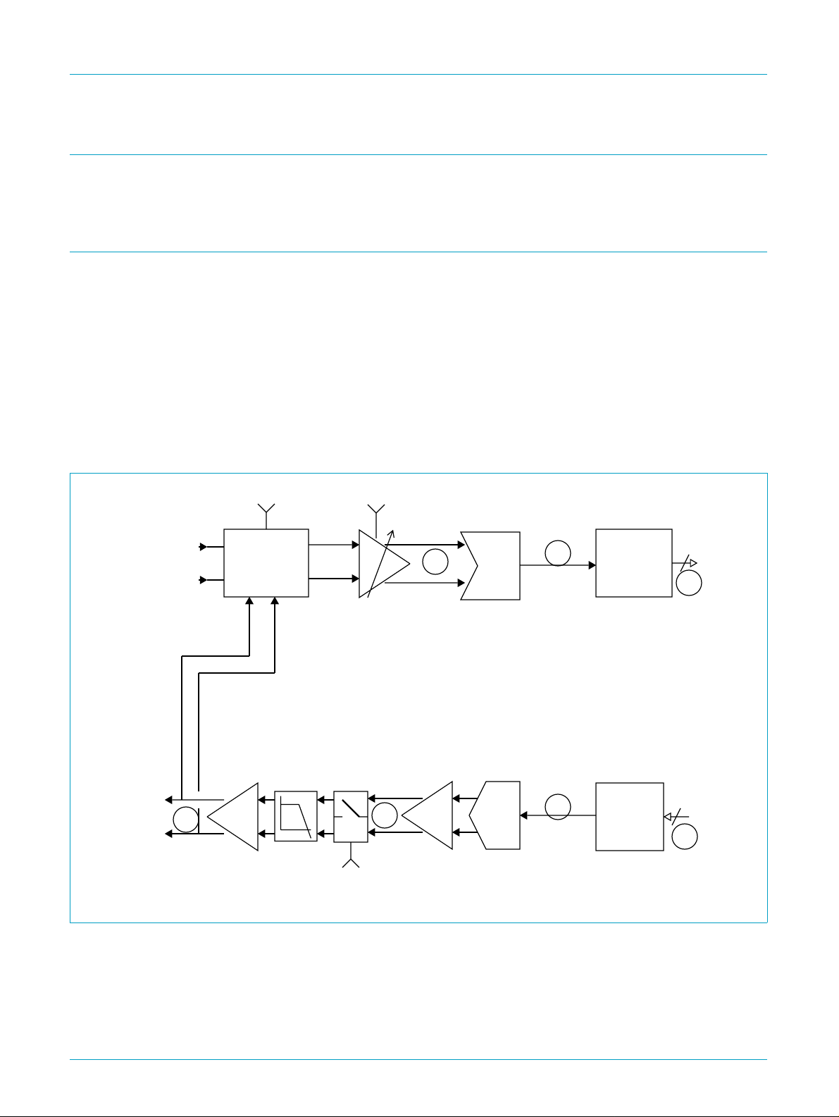
8. Telecom codec
The telecom codec contains an input channel, built up from a 64 times oversampling
sigma delta analog to digital converter (ADC) with digital decimation filters,
programmable gain and attenuation and built-in sidetone suppression circuit.
The output path consists of a digital up sample filter, a 64 time oversampling 4 bit
digital to analog converter (DAC) circuit with integrated filter followed by a differential
output driver, capable of directly driving a 600 Ω isolation transformer. The output
path includes a mute function. The telecom codec also incorporates loop back
modes, in which codec output path and the input path are connected in series. The
loop back tap and entry points are identified as circled letters in Figure 3, loop back
modes are described in the AClink register definition.
UCB1510
AC97 digital modem codec
TOUTP
TOUTN
TINP
TINN
E
sidetone_enable
SIDETONE
SUPPRESSION
CIRCUIT
ADC[3:2]
DAC Mute
ADC
J
D
DAC
H
C
DIGITAL
DECIMATION
FILTER
DIGITAL
NOISE
SHAPER
14
G
14
B
Fig 3. Telecom codec block diagram
The telecom sample rate (fst) is derived from the AC master clock and is
programmable using the sample rate registers. Not all AC97 specified sample rates
are supported, refer to Table 3 “Sampling frequencies” for details.
PCM data is transferred in the slot 5 of the AClink.
9397 750 06856
Preliminary specification Rev. 01 — 4 February 2000 5 of 32
© Philips Electronics N.V. 2000. All rights reserved.
Page 6

Philips Semiconductors
Table 3: Sampling frequencies
Sampling frequency (Hz) Register 0x40
7200 0x1C20 no recommended
8000 0x1F40 yes required
8228.57 (57600/7) 0x2024 no recommended
8400 0x20D0 no recommended
9000 0x2328 no recommended
9600 0x2580 yes required
10285.71 (72000/7) 0x282D no recommended
12000 0x2EE0 yes recommended
13714.29 (96000/7) 0x3592 yes required
16000 0x3E80 yes required
19200 0x4B00 yes recommended
24000 0x5DC0 yes recommended
48000 0xBB80 no recommended
value
UCB1510
AC97 digital modem codec
Support AC ‘97
requirements
Any programmed vlaue above 24 kHz will lead to a 24 kHz sampling rate.
Changing the sampling rate while the codec is active may lead to unpredictable
results in the ADC and DAC chains and should be avoided.
The output section of the telecom codec is designed to interface with a 600 Ω line
through an isolation transformer. The built in mute function is activated by the
DAC Mute bit in register 0x46. The output driver remains active in the mute mode,
however no output signal is produced.
8.1 Digital filters
These filters are tailored for high speed modem performance.
A voice band filter can be activated to reduce the noise in the lower frequencies.
Table 4: Filter characteristics
Parameter Condition Value
Group delay 25 samples
Pass band ripple ±0.1 dB
Out of band rejection >0.55 fs -50 dB
Pass band (no voice band filter) 0.0016 to 0.45 fs
Transition band 0.45 to 0.55 fs
Voice band filter rejection band 0-0.0018 fs 30 dB
Voice band filter cutoff frequency 0.05 fs
9397 750 06856
Preliminary specification Rev. 01 — 4 February 2000 6 of 32
© Philips Electronics N.V. 2000. All rights reserved.
Page 7
Philips Semiconductors
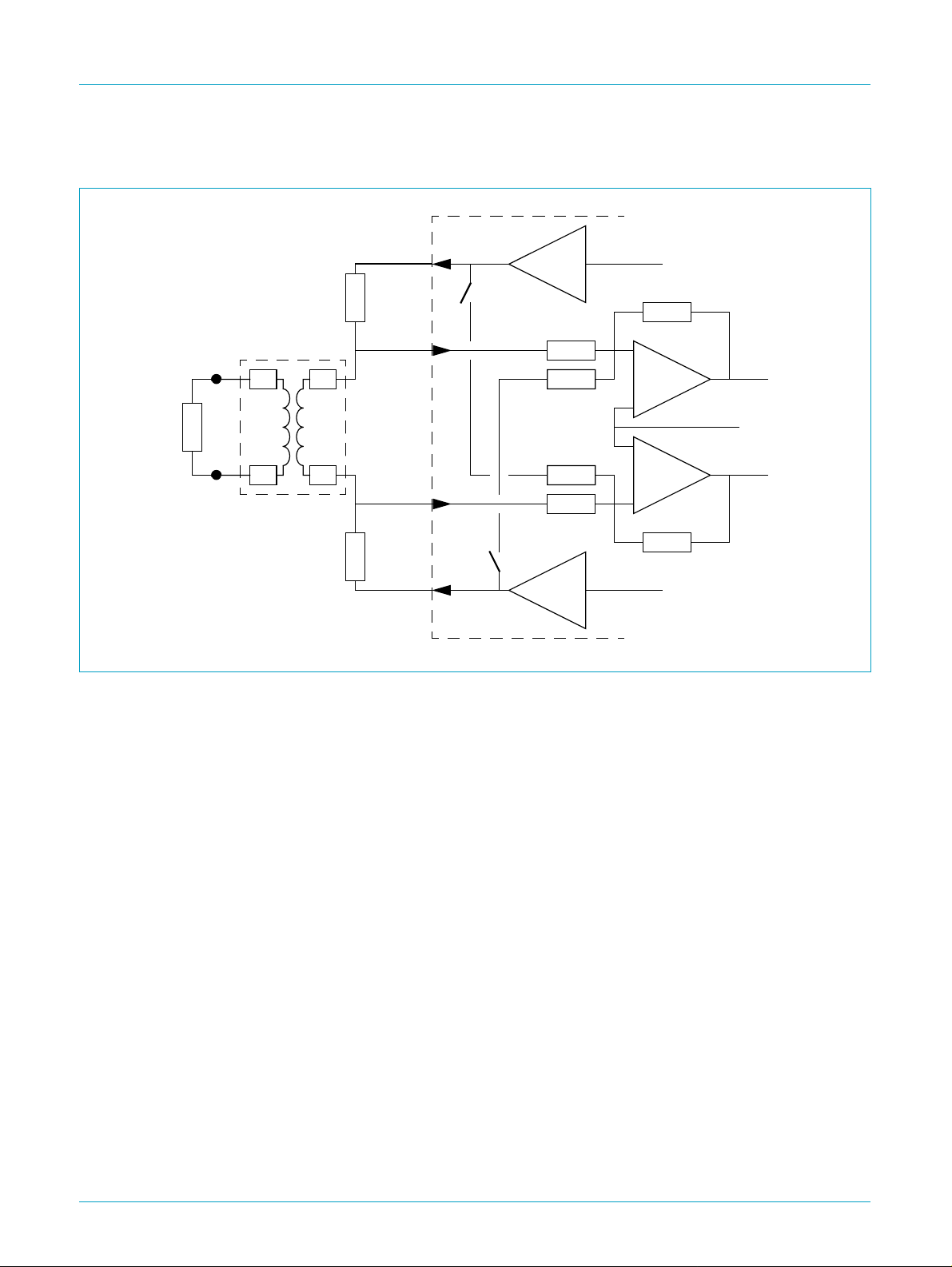
8.2 Analog interface
UCB1510
AC97 digital modem codec
UCB1510
TOUTP
A
Central Office
1:1 transformer
Rt
Rt
Ro
TINP
Ri
Rs
Rg
+
+
Rt
B
Fig 4. Typical telecom codec sidetone suppression circuit (without protection circuits).
Rt
TINN
Ro
TOUTN
An important built-in feature of the telecom codec is the sidetone suppression circuit.
The sidetone suppression circuit is activated when sidetone_enable of register 0x5A
is set.The sidetone suppression circuit subtracts part of the telecom output signal
from the telecom input signal. As a result the available dynamic range of the input
path can be more effectively utilized. If the sidetone suppression circuit is disabled,
the telecom input dynamic range can be largely occupied by the telecom output
signal.
Rs
Ri
-
Rg
The built-in side tone suppression circuit, shown in Figure 4, has a fixed subtraction
ratio, set be the resistors R
and Ri, which equals
s
600
⁄
. This ratio is calculated from
456
the following relations.
The impedance seen by the telephone line equals:
Z
line
2RtR
×=
RoRi×
++
----------------- -
t
RoRi+
, differential, in which Rtrepresents winding resistance
of the transformer, divided by 2. Assuming Ri >> Ro, then
R
line
RtRtRo600 2⁄ 300Ω==++=
single ended.
A typical transformer has 156 Ω winding impedance, thus Ro should be 144 Ω. The
ratio of the telecom input and output voltage is, therefore:
V
i(tel)
V
---------------------------------------
o(tel)
156 300 144++
156 300+
V
o(tel)
456
×=×=
-------- -
600
Proper sidetone suppression thus requires Rs/Ri to be Vi/Vo.
9397 750 06856
Preliminary specification Rev. 01 — 4 February 2000 7 of 32
© Philips Electronics N.V. 2000. All rights reserved.
Page 8
Philips Semiconductors
9. On-chip reference circuit
The UCB1510 contains an on chip reference voltage source, which generates the
bias currents and the virtual analog ground. Alternatively the UCB1510 can be driven
from an external reference voltage source.
Bias ENA
vref_external
ena
Vbg
vref_bypass
internal
bandgap
reference
voltage
circuitry
&
&
UCB1510
AC97 digital modem codec
internal
analog
ground
Fig 5. Block diagram of the reference circuit.
Two bits in the control register 0x5A determine the mode of operation of this
reference voltage circuit. vref_bypass connects the internal reference voltage to the
VREFBYP pin, while vref_external disables the internal reference voltage and
switches the UCB1510 into the external voltage reference mode.
If the internal reference voltage is connected to the VREFBYP pin, an external
capacitor could be connected to filter this reference voltage. When choosing a
capacitor, the internal impedance (around 50 kΩ) should be taken into account.
If vref_external is set, an external voltage reference connected to the VREFBYP pin
is used as the voltage reference by UCB1510.
10. Power supply strategy
Since all the control logic of the UCB1510 is powered by the V
alwaysbe present on this pin for interrupts to be possible. V
all the time although it is recommended to use the control bits to turn OFF the analog
sections.
VREFBYP
, power should
DDD
needs not be present
DDA
9397 750 06856
Preliminary specification Rev. 01 — 4 February 2000 8 of 32
© Philips Electronics N.V. 2000. All rights reserved.
Page 9

Philips Semiconductors
11. Register definition
11.1 Supported registers
Table 5: Supported registers
Register Name
0x00 to 0x3A All audio registers are ignored
0x3C Extended Modem ID
0x3E Extended Modem Status and Control
0x40 Line1 DAC/ADC Rate
0x42 and 0x44 Reserved for future use
0x46 Line1 DAC/ADC Level
0x48 and 0x4A Reserved for future use
0x4C GPIO Pin Configuration
0x4E GPIO Pin Polarity
0x50 GPIO Pin Sticky
0x52 GPIO Pin Wake-up Mask
0x54 GPIO Pin Status
0x56 Miscellaneous Modem AFE Status and Control
0x58 Ignored
0x5A Codec control
0x5C Mode control
0x5E Test control
0x5E to 0x7A Ignored
0x7C Vendor ID1
0x7E Vendor ID2
UCB1510
AC97 digital modem codec
11.2 Register detail
Shaded areas indicate read only data.
11.2.1 Extended Modem ID
Table 6: Extended Modem ID Register
Register address: 0x3C; default: N/A
Bit D15 D14 D13 D12 D11 D10 D9 D8
Symbol
Bit D7 D6 D5 D4 D3 D2 D1 D0
Symbol
Table 7: Description of Extended Modem ID bits
Bit Symbol Function/Value
D15:14 ID[1:0] {A1,A0} where A0 is the inverse polarity of the
D0 LIN1 Line 1 support indicator = 1 (i.e., Line 1 is supported).
[1] Writing this register will cause a register reset: all modem registers will then take their default values.
9397 750 06856
Preliminary specification Rev. 01 — 4 February 2000 9 of 32
ID1 ID0
polarity of XTAL_IN pin if A0 is HIGH (
0 0 0 0 LIN1
A0 pin. A1 is the inverse
A0 pin is LOW), otherwise A1 is 0.
© Philips Electronics N.V. 2000. All rights reserved.
Page 10

Philips Semiconductors
11.2.2 Extended Modem Status and Control
Table 8: Extended Modem Status and Control Register
Register address: 0x3E; default: 0xFFxx
Bit D15 D14 D13 D12 D11 D10 D9 D8
Symbol PRH PRG PRF PRE PRD PRC PRB PRA
Bit D7 D6 D5 D4 D3 D2 D1 D0
Symbol
Table 9: Description of Extended Modem status and Control bits
Bit Symbol Function/Value
D15 PRH Reserved, should be 1
D14 PRG Reserved, should be 1
D13 PRF Reserved, should be 1
D12 PRE Reserved, should be 1
D11 PRD 1 -> Line1 DAC OFF
D10 PRC 1 -> Line1 ADC OFF
D9 PRB 1 -> Line1 V
D8 PRA 1 -> GPIO OFF
D7 HDAC 0 (not supported)
D6 HADC 0 (not supported)
D5 DAC2 0 (not supported)
D4 ADC2 0 (not supported)
D3 DAC1 1 indicates Line1 DAC ready (means that the Line1 DAC and the V
D2 ADC1 1 indicates Line1 ADC ready (means that the Line1 ADC and the V
D1 MREF 1 indicates Line1 V
D0 GPIO 1 indicates GPIO ready.
UCB1510
AC97 digital modem codec
HDAC HADC DAC2 ADC2 DAC1 ADC1 MREF GPIO
OFF
REF
are enabled and ready)
are enabled and ready)
REF
up to nominal level.
REF
REF
11.2.3 Line 1 Sample Rate
Table 10: Line 1 Sample Rate Register
Register address: 0x40; default: 0x1F40
Bit D15 D14 D13 D12 D11 D10 D9 D8
Symbol SR15 SR14 SR13 SR12 SR11 SR10 SR9 SR8
Bit D7 D6 D5 D4 D3 D2 D1 D0
Symbol SR7 SR6 SR5 SR4 SR3 SR2 SR1 SR0
Refer to Table 3 “Sampling frequencies” for supported sample rates.
9397 750 06856
Preliminary specification Rev. 01 — 4 February 2000 10 of 32
© Philips Electronics N.V. 2000. All rights reserved.
Page 11

Philips Semiconductors
11.2.4 Line 1 DAC/ADC Level
Table 11: Line 1 DAC/ADC Level Register
Register address: 0x46; default: 0x8080
Bit D15 D14 D13 D12 D11 D10 D9 D8
Symbol DAC
Bit D7 D6 D5 D4 D3 D2 D1 D0
Symbol ADC
Table 12: Description of Line1 DAC/ADC Level bits
Bit Symbol Function/Value
D15 DAC mute DAC section is active, but no signal will be sent.
D7 ADC mute ADC section is active, but no signal will be sent.
D3-D2 ADC[3:2] ADC Gain (0 -> 0 dB, 1 -> 6 dB, 2 -> 12 dB, 3 -> 18 dB)
D1-D0 ADC[1:0] These bits are ignored.
UCB1510
AC97 digital modem codec
mute
ADC3 ADC2 ADC1 ADC0
mute
11.2.5 GPIO Pin Configuration
Table 13: GPIO Pin Configuration Register
Register address: 0x4C; default: 0x00FF
Bit D15 D14 D13 D12 D11 D10 D9 D8
Symbol
Bit D7 D6 D5 D4 D3 D2 D1 D0
Symbol GC7 GC6 GC5 GC4 GC3 GC2 GC1 GC0
The GPIO Pin Configuration register specifies whether a GPIO pin is configured for
input (1) or for output (0).
11.2.6 GPIO Pin Polarity
Table 14: GPIO Pin Polarity Register
Register address: 0x4E; default: 0xFFFF
Bit D15 D14 D13 D12 D11 D10 D9 D8
Symbol
Bit D7 D6 D5 D4 D3 D2 D1 D0
Symbol GP7 GP6 GP5 GP4 GP3 GP2 GP1 GP0
The GPIO Pin Polarity register defines GPIO Input Polarity (0 = Low, 1 = High) when
a GPIO pin is configured as an input.
9397 750 06856
Preliminary specification Rev. 01 — 4 February 2000 11 of 32
© Philips Electronics N.V. 2000. All rights reserved.
Page 12

Philips Semiconductors
11.2.7 GPIO Pin Sticky
Table 15: GPIO Pin Sticky Register
Register address: 0x50; default: 0x0000
Bit D15 D14 D13 D12 D11 D10 D9 D8
Symbol
Bit D7 D6 D5 D4 D3 D2 D1 D0
Symbol GS7 GS6 GS5 GS4 GS3 GS2 GS1 GS0
The GPIO Pin Sticky register defines GPIO Input Type (0 = Non-Sticky, 1 = Sticky)
when a GPIO pin is configured as input. Sticky is defined as Edge sensitive,
Non-Sticky as Level-sensitive.
GPIO inputs configured as Sticky are cleared by writing a 0 to the corresponding bit
of the GPIO Pin Status register 0x54, and by reset.
Remark: Changing GPIO control registers while a GPIO is sticky may cause
unwanted interrupts and should be done carefully.
11.2.8 GPIO Wake-up Mask
UCB1510
AC97 digital modem codec
Table 16: GPIO Wake-up Mask Register
Register address: 0x52; default: 0x0000
Bit D15 D14 D13 D12 D11 D10 D9 D8
Symbol
Bit D7 D6 D5 D4 D3 D2 D1 D0
Symbol GW7 GW6 GW5 GW4 GW3 GW2 GW1 GW0
The GPIO Pin Wake-up Mask register provides a mask for determining if an input
GPIO change will generate a wake-up or GPIO_INT (0 = No, 1 = Yes).
When the AC-link is powered down, a wake-up event will trigger the assertion of
SDIN. When the AC-link is powered up, a wake-up event will appear as
GPIO_INT = 1 on bit 0 of input slot 12.
11.2.9 GPIO Pin Status
Table 17: GPIO Pin Status Register
Register address: 0x54; default: N/A
Bit D15 D14 D13 D12 D11 D10 D9 D8
Symbol
Bit D7 D6 D5 D4 D3 D2 D1 D0
Symbol GI7 GI6 GI5 GI4 GI3 GI2 GI1 GI0
The GPIO Status register reflects the state of all GPIO pins (inputs and outputs) on
slot 12.
When the GPIO is an output pin, the value set on slot #12 is transmitted directly to the
pin. When the GPIO pin is a non-sticky input, the status of the pin is accessible in
read mode. When the GPIO is a sticky Input, a transition, either from high to low
(polarity = 0) or from low-to-high (polarity = 1), will assert the corresponding GI bit
to 1. The GI bit will remain asserted until it is cleared by a write of 0.
9397 750 06856
Preliminary specification Rev. 01 — 4 February 2000 12 of 32
© Philips Electronics N.V. 2000. All rights reserved.
Page 13

Philips Semiconductors
11.2.10 Miscellaneous Modem AFE Status and Control
Table 18: Miscellaneous Modem AFE Status and Control Register
Register address: 0x56; default: 0x0000
Bit D15 D14 D13 D12 D11 D10 D9 D8
Symbol MLNK reserved, should be 0x0
Bit D7 D6 D5 D4 D3 D2 D1 D0
Symbol reserved, should be 0x0 L1B2 L1B1 L1B0
Table 19: Description of Miscellaneous Modem AFE Status and Control bits
Bit Symbol Function/Value
D13 MLNK 1 -> AClink goes to sleep.
D[2:0] L1B[2:0] Line1 loop back modes (refer to Table 20).
Table 20: Loop back modes
See Figure 3.
Mode Description
0 Disabled
1 ADC loop back (incoming analog signal is amplified, digitized, down-sampled,
2 Local analog loop back (digital signal is up-sampled, converted to analog,
3 DAC loop back (digital signal is up-sampled, converted to analog, LOOPED
4 Remote analog loop back (incoming analog signal is amplified, LOOPED,
7 Digital loop back: signal is captured from the AC-link and sent back as is. Slot
UCB1510
AC97 digital modem codec
LOOPED, up-sampled, converted to analog, amplified/filtered) (G) to (B) loop.
amplified/filtered, LOOPED, amplified, digitized, down-sampled, sent back) (E)
to (J) loop.
digitized, down-sampled, sent back) (E) to (J) loop. Same as mode 2.
amplified/filtered, sent back) (J) to (D) loop.
request for slot#5 is controlled according to the programmed sampling rate.
9397 750 06856
Preliminary specification Rev. 01 — 4 February 2000 13 of 32
© Philips Electronics N.V. 2000. All rights reserved.
Page 14

Philips Semiconductors
11.2.11 Vendor Specific Codec Control
Table 21: codec_control Register
Register address: 0x5A; default: 0x0400
Bit D15 D14 D13 D12 D11 D10 D9 D8
Symbol AC ME VE VB
Bit D7 D6 D5 D4 D3 D2 D1 D0
Symbol 0 0 0SE0 0 0VF
Table 22: codec_control bits
Bit Symbol Function/Value
D12 AC adc_clip, in read mode, this bit indicates clipping in the line1 ADC.
D10 ME reserved, should be 1
D9 VE vref_external, overwrites VB
D8 VB vref_bypass
D[7:5],
D[3:1]
D4 SE sidetone_enable
D0 VF voice_filter:1->enable voice band digital filter.
UCB1510
AC97 digital modem codec
This indicator is sticky and should be cleared by writing it with a 0.
0 Bits marked ‘0’ are reserved for future use and should be programmed
with 0.
11.2.12 Vendor Specific Mode Control
Table 23: mode_control Register
Register address: 0x5C; default: 0x0000
Bit D15 D14 D13 D12 D11 D10 D9 D8
Symbol reserved: 0x0
Bit D7 D6 D5 D4 D3 D2 D1 D0
Symbol 0 0 0 0 BITSTREAM
[1] Bits marked 0 are reserved for future use and should be programmed with 0.
Table 24: mode_control bits
Bit Symbol Function/Value
D0 BITSTREAM line1 ADC bitstream data is sent directly to IO4. The associated
clock is sent to IO6.
11.2.13 Vendor specific Test Control
Table 25: Test_control Register
Register address: 0x5E; default: N/A
Bit D15 D14 D13 D12 D11 D10 D9 D8
Symbol
Bit D7 D6 D5 D4 D3 D2 D1 D0
Symbol
This register cannot be reset. It has no effect until the IC is put in vendor test mode
(see Table 29 “Mode selection with AC pins”).
9397 750 06856
Preliminary specification Rev. 01 — 4 February 2000 14 of 32
© Philips Electronics N.V. 2000. All rights reserved.
Page 15

Philips Semiconductors
11.2.14 Vendor ID1
Table 26: Vendor ID1 Register
Register address: 0x7C; default: 0x5053
Bit D15 D14 D13 D12 D11 D10 D9 D8
Symbol
Bit D7 D6 D5 D4 D3 D2 D1 D0
Symbol
11.2.15 Vendor ID2
Table 27: Vendor ID2 Register
Register address: 0x7E; default: 0x4301
Bit D15 D14 D13 D12 D11 D10 D9 D8
Symbol
Bit D7 D6 D5 D4 D3 D2 D1 D0
Symbol
UCB1510
AC97 digital modem codec
0 1 0 1 0 0 0 0
0 1 0 1 0 0 1 1
0 1 0 0 0 0 1 1
0 0 0 0 0 0 0 1
11.3 Register reset modes
11.3.1 Warm reset
When a warm reset is activated, MLNK is set to 0 but the other registers retain their
values. If the codec is primary, the BIT_CLK is started and stabilized after 200 ms.
11.3.2 Cold reset
When a cold reset is activated, MLNK is set to 0 and all registers are programmed to
their default values. If the codec is primary, the BIT_CLK is started and stabilized
after 200 ms.
11.3.3 Register reset
A register reset causes all registers to return to their default values. Initiated by a
write to register 0x3C.
9397 750 06856
Preliminary specification Rev. 01 — 4 February 2000 15 of 32
© Philips Electronics N.V. 2000. All rights reserved.
Page 16

Philips Semiconductors
12. AC97 interface
12.1 Control register data transfer
The AClink frames is made of 13 slots. Slot0 is a 16-bit long tag slot, the remaining 12
slots are 20-bit long data transfer.
SYNC
UCB1510
AC97 digital modem codec
48KHz
Clock:12.288MHz
SDOUT (SLOT #)
16 bits
#0 #1 #2 #3 #4 #5 #6 #7 #8 #9 #10 #11 #12 #0
SLOT #0: TAG
Fig 6. AClink frame slot definition
Register update is done at the end of slot 2. The new register value is effective
thereafter.
Slot #0 and slot #3 to #12 are shared by all codecs (primary and secondary). Multiple
codecs using the same slot cannot be used at the same time. Slot #1 and slot #2 are
used for register transfer and are codec specific. Addressing is defined in the
Tag slot #0: The UCB1510 will send a 1 as Tag slot bit 15 whenever the AClink is
active (MLNK is 0).
20bits
SLOT #2: CMD DATA
SLOT #1: CMD ADDR
SLOT #3 & #4:
not supported by UCB1510
SLOT #5: LINE1 DAC
SLOT #6.. #9:
SLOT #12: I/O CTRL
not supported by UCB1510
9397 750 06856
Preliminary specification Rev. 01 — 4 February 2000 16 of 32
© Philips Electronics N.V. 2000. All rights reserved.
Page 17

Philips Semiconductors
SYNC
BIT_CLK
UCB1510
AC97 digital modem codec
16 BIT_CLKs
SDOUT
(bit numbers)
1514131211109876 543210
0
Bit 15: If 1 then Valid Frame; if 0 then frame can be ignored
Bit 14: If 1 then Slot #1 (CMD_ADDR) is valid
Bit 13: If 1 then Slot #2 (CMD_DATA) is valid
Bit 12: If 1 then Slot #3 is valid - should be 0 for UCB1510
Fig 7. Tag slot bit definition (controller to codec)
16 BIT_CLKs
SYNC
19 18 17 16 15
SLOT #0
Bit 11: If 1 then Slot #4 is valid - should be 0 for UCB1510
Bit 10: If 1 then Slot #5 (Line 1) is valid
Bit 9: If 1 then Slot #6 is valid - should be 0 for UCB1510
Bit 8: If 1 then Slot #7 is valid - should be 0 for UCB1510
Bit7: If 1 then Slot #8 is valid - should be 0 for UCB1510
Bit 6: If 1 then Slot #9 is valid - should be 0 for UCB1510
Bit 5: If 1 then Slot #10 is valid - should be 0 for UCB1510
Bit 4: If 1 then SLot #11 s valid - should be 0 for UCB1510
Bit3: If 1 then Slot #12 (I/O Control) is valid
Bit 2: Unused, set to 0
Bit 1: Codec ID A1
SLOT #1
Bit 17: Register index[5]
Bit 19: Read/Write (1-> read)
Bit 18: Register index[6]
Bit 0: Codec ID A0
Bit 16: Register index[4]
Bit 15: Register index[3]
BIT_CLK
SDIN
(bit numbers)
1514131211109876 543210
0
SLOT #0
Bit 15: If 1 then Valid Frame; if 0 then frame can be ignored
Bit 14: If 1 then Slot #1 (CMD_ADDR) is valid
Bit 13: If 1 then Slot #2 (CMD_DATA) is valid
Bit 12: 0
Bit 11: 0
Bit 10: If 1 then Slot #5 is valid
Bit 9: 0
Bit 8: 0
Bit7: I0
Bit 6: 0
Bit 5: 0
Bit 4: 0
Bit3: If 1 then Slot #12 (I/O Control) is valid
19 18 17 16 15
SLOT #1
Bit 17: Register index[5]
Bit 19: Register_read
Bit 2: Unused, set to 0
Bit 1: 0
Bit 18: Register index[6]
Bit 0: 0
Bit 16: Register index[4]
Bit 15: Register index[3]
Fig 8. Tag slot bit definition (codec to controller)
9397 750 06856
Preliminary specification Rev. 01 — 4 February 2000 17 of 32
© Philips Electronics N.V. 2000. All rights reserved.
Page 18

Philips Semiconductors
UCB1510
AC97 digital modem codec
12.2 Codec addressing
Table 28: Codec addressing examples
CMD ADDR CMD DATA Codec ID
slot #0
bit 14
0 0 00 x idle No register data is transferred, slots1
1 x 00 1 primary read Read for primary codec register
1 1 00 0 primary write Write to a primary codec register
x x 01 1 secondary read Read from the 01 secondary codec
x x 11 0 secondary write Write to a 11 secondary codec register
slot #0
bit 13
(A1, A0)
slot #0
bits 1 and 0
12.2.1 Primary codec addressing
For addressing a primary codec, bits 1 and 0 of the Tag slot (codec ID A1 and A0)
should be 0. The bits 13 and 14 are used for register data transfer. When the
controller is not sending/receiving control data, it should be addressing the primary
codec. When writing to a register, the bits 14 and 13 (ADDR and DATA valid) should
be set to 1. When reading from a register, only the bit 14 is required to be 1.
Read/Write Transfer Description
slot #1
bit 19
and 2 are not valid
register
12.2.2 Secondary codec addressing
When the Codec ID (A1,A0) is not 00, the controller is addressing a secondary codec
in a read or write sequence. The direction is defined in the slot 1 read/write bit (bit
19).
12.3 PCM sample transfer
Since the AClink frame frequency is defined to be 48kHz, exchanging samples with
the controller at a different sampling rate requires the support of on demand sample
transfer (slot request). The UCB1510 will send samples to the controller and assert
the slot 5 valid bit in the slot#0 (bit10)of the AClink frame. When it needs a new
sample from the controller, it will put a 0 on the slot5req bit in the slot#1 (bit9) of the
AClink frame. When the slot5req bit is 1, it indicates to the controller that no new
sample is needed. When the DAC is not active, the slot5req bit is kept at 0.
9397 750 06856
Preliminary specification Rev. 01 — 4 February 2000 18 of 32
© Philips Electronics N.V. 2000. All rights reserved.
Page 19

Philips Semiconductors
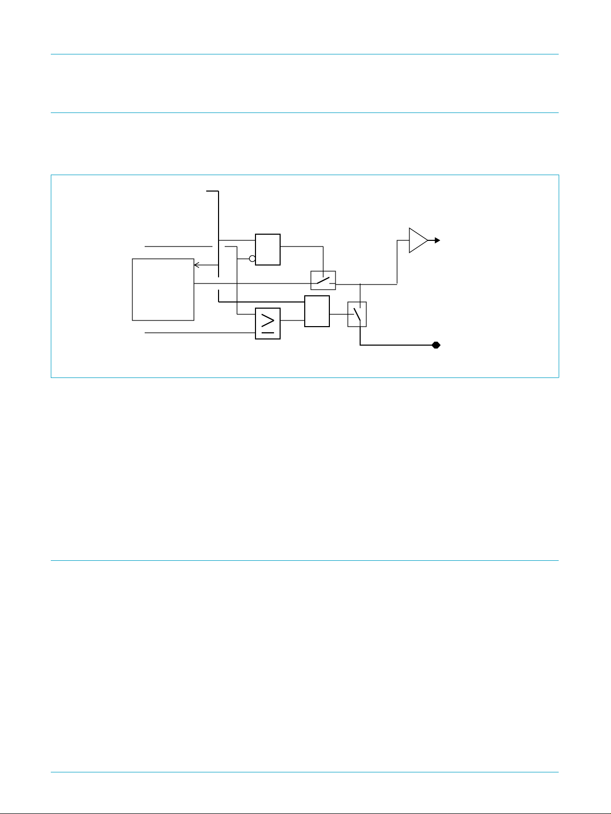
12.4 Interrupt request from UCB1510
MLNK
BIT_CLK
SDIN
Fig 9. Setting the SDIN for interrupt request
12.4.1 When BIT_CLK is running
The AClink is active and the interrupt request is transmitted by setting the interrupt bit
of slot 12 in the AClink frame.
UCB1510
AC97 digital modem codec
Interrupt request
Interrupt request
is enabled
If UCB1510 is configured as a primary codec, this is the case when MLNK is set to 0.
If UCB1510 is configured as a secondary codec, this is the case whether MLNK is set
to 0 or 1.
12.4.2 When BIT_CLK is stopped
In order to request an interrupt, the UCB1510 will assert the SDIN pin, if MLNK is set
to 1. BIT_CLK is not needed for this to happen. This applies when UCB1510 is used
as a primary or secondary codec.
If UCB1510 is configured as a primary codec, BIT_CLK is stopped as a result of
MLNK being set to 1.
If UCB1510 is configured as a secondary codec, BIT_CLK is stopped when the
controller shuts down the primary codec. For UCB1510 to generate interrupt while
BIT_CLK is stopped, MLNK has to be set to 1 before BIT_CLK is stopped.
After BIT_CLK is stopped, SDIN will be brought to 0, unless an interrupt asserts it
to 1. It is recommended that a level triggered interrupt detection is used in case the
interrupt request is asserted at the same time BIT_CLK is stopped.
12.5 Wake-up request to the UCB1510
A cold reset will program the registers to their default value and will wake up the
AClink.
When the AClink is not active (no BIT_CLK present), a rising SYNC will cause a
warm reset. If MLNK is set to 1, a rising RESET will also cause a warm reset. After a
warm reset, MLNK will be reset to 0.
9397 750 06856
Preliminary specification Rev. 01 — 4 February 2000 19 of 32
© Philips Electronics N.V. 2000. All rights reserved.
Page 20

Philips Semiconductors
13. General purpose I/O
The UCB1510 has 8 programmable digital input/output (I/O) pins. These pins can be
independently programmed for polarity, value, direction and interrupt through the
GPIO control registers.
14. Interrupt generation
The UCB1510 contains a programmable interrupt control block.
The internal interrupt signal presents the 'OR' function of all interrupt status bits and
can be used to give an interrupt to the system controller using the AClink interrupt
protocol
The interrupt controller is implemented asynchronously. This provides the possibility
to generate interrupts when BIT_CLK is stopped, e.g. an interrupt can be generated
in power down mode, when the state of one of the IO pins changes (e.g. ring detect).
15. Reset circuit and mode selection
UCB1510
AC97 digital modem codec
The AC97 specification rev 2.1 describes a number of states and reset functions for a
modem codec either in primary or secondary codec.
15.1 Resets
15.1.1 Pulling the PON pin LOW
The PON pin acts as a hardware reset and is typically connected to a power
detection circuit.
15.1.2 Activating the RESET pin
Pulling the RESET pin low will start a cold or a warm reset sequence.
If the circuit is active (MLNK = 0). A cold reset is started. The reset sequence will end
after the rising edge of RESET. Only then will the AClink be available. Vendor test
modes are inactive as soon as the reset sequence starts so that mode sensing is
possible.
If the MLNK bit is set when the RESET pin is pulled low, a warm reset is activated
when RESET goes high again.
15.1.3 Activating the SYNC pin when AClink is inactive
When the AClink is not active (no BIT_CLK present), a rising SYNC will cause a
warm reset.
15.1.4 Writing reg 0x3C
When written, the reg 0x3C will initiate a register reset. All registers are set to their
default values.
9397 750 06856
Preliminary specification Rev. 01 — 4 February 2000 20 of 32
© Philips Electronics N.V. 2000. All rights reserved.
Page 21

Philips Semiconductors
15.2 Vendor test modes
When starting a RESET pin induced cold reset, the AClink pins are sensed for
Vendor Test mode selection. BIT_CLK does not need to be running at that moment
Table 29: Mode selection with AC pins
SYNC SDOUT Mode
0 0 Normal mode, the AClink is operating properly.
0 1 ATE test mode. All AClink pins are set to input thus allowing
1 0 Vendor test mode.
1 1 ATE test mode.
When the vendor test mode is activated, the vendor test register takes action. This
mode is for test only and should not be used in normal operation. Exiting this mode
requires a cold reset.
15.3 Primary/secondary codec selection
UCB1510
AC97 digital modem codec
board level JTAG testing.
16. Limiting values
Secondary codec implementation is selected by wiring the A0 pin low.
When A0 is low (A0 is 1), the XTAL_IN is used as A1 thus allowing ‘01’ and ‘11’ as
secondary addresses. ‘10’ is not possible. The ID register will then reflect the A1,A0.
Details can be found in the description of register 0x3C.
When the UCB1510 is a secondary codec, it derives its internal clock from BIT_CLK.
BITCLK is therefore configured as input.
Table 30: Limiting values
In accordance with the Absolute Maximum Rating System (IEC 60134).
Symbol Parameter Conditions Min Max Unit
V
DD
V
i
V
o
I
i(d)
I
o(d)
I
o
T
stg
[1] Stresses above those listed under Absolute Maximum Ratings may cause permanent damage to the
device. This is a stress rating only and functional operation of the device at these or any conditions
other than those described in the Absolute Maximum Rating section of this specification is not implied
[2] Parameters are valid over the ambient operating temperature unless otherwise specified. All voltages
are with respect to V
supply voltage −0.5 +4.0 V
DC input voltage −0.5 VDD+ 0.5 V
DC output voltage − VDD+ 0.5 V
diode input current − 10 mA
diode output current − 10 mA
continuous output current,
digital outputs
storage temperature −55 +150 °C
, unless otherwise noted.
SSD
− 4mA
[1].[2]
9397 750 06856
Preliminary specification Rev. 01 — 4 February 2000 21 of 32
© Philips Electronics N.V. 2000. All rights reserved.
Page 22

Philips Semiconductors
UCB1510
AC97 digital modem codec
17. Thermal characteristics
Table 31: Thermal characteristics
Symbol Parameter Conditions Value Unit
R
th(j-a)
thermal resistance from junction
55 K/W
to ambient in free air
18. Static characteristics
Table 32: Static characteristics
V
SSD=VSSA1
Symbol Parameter Conditions Min Typ Max Unit
V
DDD
V
DDA1
I
DDD
I
DDA1
I
DDA2
V
IL
V
IH
V
OL
V
OH
f
BIT_CLK
T
amb
=0V; T
=25°C; all voltages referenced to V
amb
; unless otherwise specified.
SSD
digital supply voltage 3.0 3.3 3.6 V
analog supply voltage 3.0 3.3 3.6 V
digital supply current
digital supply current full functionality
analog supply current Power down,
[1]
− 19 − mA
[1]
−−mA
t.b.d.
only oscillator is on
LOW level input voltage −0.5 − +0.2V
HIGH level input voltage 0.8V
DDD
− 0.5V
DDD
DDD
V
V
LOW level output voltage IOL=4mA −−0.4 V
HIGH level output voltage IOH= 4 mA 0.8V
DDD
−−V
serial interface clock frequency 12.288 MHz
operating ambient temperature −20 − 70 °C
[1] Indicative value measured during the initial characterization.
9397 750 06856
Preliminary specification Rev. 01 — 4 February 2000 22 of 32
© Philips Electronics N.V. 2000. All rights reserved.
Page 23

Philips Semiconductors
UCB1510
AC97 digital modem codec
19. Dynamic characteristics
Table 33: Dynamic characteristics
V
SSD=VSSA
specified.
Symbol Parameter Conditions Min Typ Max Unit
Telecom input
f
st
V
i(rms)
V
i(bias)
α
i
Z
i
S/N signal-to-noise ratio 60 75 − dB
THD total harmonic distortion −−75 −60 dB
LE
(d)(ADC)
RES codec resolution − 14 − bit
PBRR pass-band ripple rejection f
SBR
vti
SBR
sht
D
offset
S
sup
Telecom output
f
st
V
o(rms)
V
o(bias)
RES codec resolution − 14 − bit
S/N signal-to-noise ratio 60 75 − dB
THD total harmonic distortion −−75 − dB
PBRR pass-band ripple rejection
SBR stop-band rejection f
OBR
(rms)
Z
o(load)
E
offset
=0V; V
[1]
DDD=VDDA
= 3.3 V±10%; T
=25°C; V
amb
I(ref)
= 1.2 V; f
BIT_CLK
= 12.288 MHz; unless otherwise
sample frequency − 8 − kHz
input voltage (RMS value) differentially applied to TINN
330 370 410 mV
and TINP;ADC[3:2] = 1 (6 dB)
in register 0x46
DC bias voltage TINN/TINP 1.2 − 1.6 V
input gain 0 6 18 dB
input gain step size 2 LSBs ignored, Bit 3 step 468dB
input impedance 25 −−kΩ
ADC differential linearity
−−2 LSB
error
plt<fsig<fpht
f
vht<fsig<fpht
; no voice filter
; voice filter
[3],[6]
−−1.2 dB
[3],[6]
−−1.2 dB
activated
stop-band rejection f
sig<fvti
f
sht<fsig
; voice filter activated
[3],[6]
30 −−dB
[3],[6]
50 −−dB
digital offset no signal applied to input −−50 LSB
sidetone suppression
effectiveness
600 Ω line impedance;
1:1 transformer with 156 Ω
20 −−dB
winding resistance
[2]
sample frequency − 8 − kHz
output voltage (RMS value) differentially measured
1.35 − 1.85 V
between TOUTP and TOUTN
DC bias voltage TOUTP/TOUTN; telecom O/P
1.2 − 1.6 V
path enabled
[4],[6]
−−1.2 dB
[4],[6]
50 −−dB
−−25 mV
out-of-band rejection (RMS
sht
f>f
<f<f
st
st
value)
load impedance 600 −−Ω
offset error
[5]
−−100 mV
9397 750 06856
Preliminary specification Rev. 01 — 4 February 2000 23 of 32
© Philips Electronics N.V. 2000. All rights reserved.
Page 24

Philips Semiconductors
UCB1510
AC97 digital modem codec
Table 33: Dynamic characteristics
V
SSD=VSSA
=0V; V
DDD=VDDA
…continued
= 3.3 V±10%; T
=25°C; V
amb
I(ref)
= 1.2 V; f
BIT_CLK
= 12.288 MHz; unless otherwise
specified.
Symbol Parameter Conditions Min Typ Max Unit
On-chip reference circuit
V
i(ref)
reference voltage applied to
1.0 1.2 1.4 V
VREFBYP
t
STRTU
start-up time of internal
−−1000 ns
reference voltage circuit
Xtal oscillator
f
Z
xtal
xtal
Operating frequency 12.288 MHz
start-up time of internal
10 kΩ
reference voltage circuit
AClink control register data transfer
f
acclk
D
acclk
CLK input frequency 0 12.288 MHz
CLK duty factor − 50 − %
Reset circuit
t
W(NRESET)
t
W(rst)
[1] Additional test conditions: Fsample = 8 kHz; input signal 1 kHz, 300 mV (RMS); Line1_ADC_ON = 1; TEL_VOICE_ENA = 0,
input gain +6 dB
[2] Additional test conditions: Fsampling 8 kHz; 0 dB output attenuation; 90% of digital full scale input voltage; 1200 Ω load.
[3] See Figure 10.
[4] See Figure 11.
[5] Deviation of the analog output from 0, with 0 code input to telecom output path.
[6] All curves repeat around the sample frequency fsa or fst for telecom codec.
RESET pulse width 5 −−ns
internal reset pulse width 32 t
CLK
− ns
0dB
SBRvti
SBRsht
Fplt
Fvlt Fvht
PBRR
Voice filter enabled
Fpht
Fsht
f
f
f
f
f
plt
pht
sht
vlt
vht
0.0016 fst×=
0.42 fst×=
0.6 fst×=
0.018 fst×=
0.05 fst×=
Fig 10. Telecom input frequency response
9397 750 06856
Preliminary specification Rev. 01 — 4 February 2000 24 of 32
© Philips Electronics N.V. 2000. All rights reserved.
Page 25

Philips Semiconductors
UCB1510
AC97 digital modem codec
0dB
SBR
Fplt Fpht
Fig 11. Telecom output frequency response
PBRR
Frequency [Hz]
f
f
f
plt
pht
sht
0.0016 fst×=
0.42 fst×=
0.6 fst×=
Fsht
9397 750 06856
Preliminary specification Rev. 01 — 4 February 2000 25 of 32
© Philips Electronics N.V. 2000. All rights reserved.
Page 26

Philips Semiconductors
20. Package outline
UCB1510
AC97 digital modem codec
SSOP28: plastic shrink small outline package; 28 leads; body width 5.3 mm
D
c
y
Z
28 15
A
2
A
pin 1 index
1
SOT341-1
E
H
E
Q
L
p
L
(A )
A
X
v M
A
A
3
θ
114
b
e
DIMENSIONS (mm are the original dimensions)
UNIT A1A2A
Note
1. Plastic or metal protrusions of 0.20 mm maximum per side are not included.
A
max.
0.21
mm
2.0
OUTLINE
VERSION
SOT341-1 MO-150AH
0.05
1.80
1.65
IEC JEDEC EIAJ
0.25
b
0.38
0.25
p
cD
0.20
0.09
3
p
0 2.5 5 mm
(1)E(1) (1)
10.4
10.0
REFERENCES
Fig 12. SSOP28 package; SOT341-1.
detail X
w M
scale
eHELLpQZywv θ
5.4
0.65 1.25
5.2
7.9
7.6
1.03
0.63
0.9
0.7
EUROPEAN
PROJECTION
0.13 0.10.2
1.1
0.7
ISSUE DATE
93-09-08
95-02-04
o
8
o
0
9397 750 06856
© Philips Electronics N.V. 2000. All rights reserved.
Preliminary specification Rev. 01 — 4 February 2000 26 of 32
Page 27

Philips Semiconductors
21. Soldering
21.1 Introduction to soldering surface mount packages
This text gives a very brief insight to a complex technology. A more in-depth account
of soldering ICs can be found in our
Packages
There is no soldering method that is ideal for all surface mount IC packages. Wave
soldering is not always suitable for surface mount ICs, or for printed-circuit boards
with high population densities. In these situations reflow soldering is often used.
21.2 Reflow soldering
Reflow soldering requires solder paste (a suspension of fine solder particles, flux and
binding agent) to be applied to the printed-circuit board by screen printing, stencilling
or pressure-syringe dispensing before package placement.
Several methods exist for reflowing; for example, infrared/convection heating in a
conveyor type oven. Throughput times (preheating, soldering and cooling) vary
between 100 and 200 seconds depending on heating method.
UCB1510
AC97 digital modem codec
Data Handbook IC26; Integrated Circuit
(document order number 9398 652 90011).
Typical reflow peak temperatures range from 215 to 250 °C. The top-surface
temperature of the packages should preferable be kept below 230 °C.
21.3 Wave soldering
Conventional single wave soldering is not recommended for surface mount devices
(SMDs) or printed-circuit boards with a high component density, as solder bridging
and non-wetting can present major problems.
To overcome these problems the double-wave soldering method was specifically
developed.
If wave soldering is used the following conditions must be observed for optimal
results:
Use a double-wave soldering method comprising a turbulent wave with high
•
upward pressure followed by a smooth laminar wave.
For packages with leads on two sides and a pitch (e):
•
– larger than or equal to 1.27 mm, the footprint longitudinal axis is preferred to be
parallel to the transport direction of the printed-circuit board;
– smaller than 1.27 mm, the footprint longitudinal axis must be parallel to the
transport direction of the printed-circuit board.
The footprint must incorporate solder thieves at the downstream end.
For packages with leads on four sides, the footprint must be placed at a 45° angle
•
to the transport direction of the printed-circuit board. The footprint must
incorporate solder thieves downstream and at the side corners.
During placement and before soldering, the package must be fixed with a droplet of
adhesive. The adhesive can be applied by screen printing, pin transfer or syringe
dispensing. The package can be soldered after the adhesive is cured.
9397 750 06856
Preliminary specification Rev. 01 — 4 February 2000 27 of 32
© Philips Electronics N.V. 2000. All rights reserved.
Page 28

Philips Semiconductors
Typical dwell time is 4 seconds at 250 °C. A mildly-activated flux will eliminate the
need for removal of corrosive residues in most applications.
21.4 Manual soldering
Fix the component by first soldering two diagonally-opposite end leads. Use a low
voltage (24 V or less) soldering iron applied to the flat part of the lead. Contact time
must be limited to 10 seconds at up to 300 °C.
When using a dedicated tool, all other leads can be soldered in one operation within
2 to 5 seconds between 270 and 320 °C.
21.5 Package related soldering information
Table 34: Suitability of surface mount IC packages for wave and reflow soldering
Package Soldering method
BGA, LFBGA, SQFP, TFBGA not suitable suitable
HBCC, HLQFP, HSQFP, HSOP, HTQFP,
HTSSOP, SMS
PLCC
LQFP, QFP, TQFP not recommended
SSOP, TSSOP, VSO not recommended
UCB1510
AC97 digital modem codec
methods
Wave Reflow
not suitable
[3]
, SO, SOJ suitable suitable
[2]
[3] [4]
[5]
suitable
suitable
suitable
[1]
[1] All surface mount (SMD) packages are moisture sensitive. Depending upon the moisture content, the
maximum temperature (with respect to time) and body size of the package, there is a risk that internal
or external package cracks may occur due to vaporization of the moisture in them (the so called
popcorn effect). For details, refer to the Drypack information in the
Circuit Packages; Section: Packing Methods
[2] These packages are not suitable for wavesoldering as a solder joint between the printed-circuit board
and heatsink (at bottom version) can not be achieved, and as solder may stick to the heatsink (on top
version).
[3] If wave soldering is considered, then the package must be placed at a 45° angle to the solder wave
direction. The package footprint must incorporate solder thieves downstream and at the side corners.
[4] Wave soldering is only suitable for LQFP, QFP and TQFP packages with a pitch (e) equal to or larger
than 0.8 mm; it is definitely not suitable for packages with a pitch (e) equal to or smaller than 0.65 mm.
[5] Wave soldering is only suitablefor SSOP and TSSOP packages with apitch(e)equal to or larger than
0.65 mm; it is definitely not suitable for packages with a pitch (e) equal to or smaller than 0.5 mm.
22. Revision history
Table 35: Revision history
Rev Date CPCN Description
01 991111 - Converted to DBII format.
The format of this specification has been redesigned to comply with Philips Semiconductors’
new presentation and information standard.
Data Handbook IC26; Integrated
.
9397 750 06856
Preliminary specification Rev. 01 — 4 February 2000 28 of 32
© Philips Electronics N.V. 2000. All rights reserved.
Page 29

Philips Semiconductors
AC97 digital modem codec
23.Data sheet status
UCB1510
Datasheet status Product status Definition
Objective specification Development This data sheet contains the design target or goal specifications for product development. Specification may
change in any manner without notice.
Preliminary specification Qualification This data sheet contains preliminary data, and supplementary data will be published at a later date. Philips
Semiconductors reserves the right to make changes at any time without notice in order to improve design and
supply the best possible product.
Product specification Production This data sheet contains final specifications. Philips Semiconductors reserves the right to make changes at any
time without notice in order to improve design and supply the best possible product.
[1] Please consult the most recently issued data sheet before initiating or completing a design.
24.Definitions
Short-form specification —Thedatainashort-formspecificationis
extractedfromafulldatasheetwiththesametypenumberandtitle.For
detailed information see the relevant data sheet or data handbook.
Limiting values definition —Limitingvaluesgivenareinaccordancewith
theAbsoluteMaximumRatingSystem(IEC60134).Stressaboveoneor
moreofthelimitingvaluesmaycausepermanentdamagetothedevice.
Thesearestressratingsonlyandoperationofthedeviceattheseoratany
otherconditionsabovethosegivenintheCharacteristicssectionsofthe
specificationisnotimplied.Exposuretolimitingvaluesforextendedperiods
may affect device reliability.
Application information —Applicationsthataredescribedhereinforany
oftheseproductsareforillustrativepurposesonly.PhilipsSemiconductors
makenorepresentationorwarrantythatsuchapplicationswillbesuitablefor
the specified use without further testing or modification.
[1]
25.Disclaimers
Life support —Theseproductsarenotdesignedforuseinlifesupport
appliances,devices,orsystemswheremalfunctionoftheseproductscan
reasonablybeexpectedtoresultinpersonalinjury.PhilipsSemiconductors
customersusingorsellingtheseproductsforuseinsuchapplicationsdoso
attheirownriskandagreetofullyindemnifyPhilipsSemiconductorsforany
damages resulting from such application.
Right to make changes —PhilipsSemiconductorsreservestherightto
makechanges,withoutnotice,intheproducts,includingcircuits,standard
cells,and/orsoftware,describedorcontainedhereininordertoimprove
design and/or performance. Philips Semiconductors assumes no
responsibilityorliabilityfortheuseofanyoftheseproducts,conveysno
licenceortitleunderanypatent,copyright,ormaskworkrighttothese
products,andmakesnorepresentationsorwarrantiesthattheseproducts
arefreefrompatent,copyright,ormaskworkrightinfringement,unless
otherwise specified.
9397 750 06856
© Philips Electronics N.V. 2000 All rights reserved.
Preliminary specification Rev. 01 — 4 February 2000 29 of 32
Page 30

Philips Semiconductors
AC97 digital modem codec
Philips Semiconductors - a worldwide company
UCB1510
Argentina: see South America
Australia: Tel.+61297048141,Fax.+61297048139
Austria: Tel. +43160101, Fax.+431601011210
Belarus: Tel. +37517 220 0733, Fax.+37517 220 0773
Belgium: see The Netherlands
Brazil:see South America
Bulgaria: Tel. +359268 9211, Fax.+359268 9102
Canada: Tel. +18002347381
China/Hong Kong: Tel. +852 2 3197888, Fax.+8522 3197700
Colombia: see South America
Czech Republic: see Austria
Denmark: Tel. +453 2882636, Fax.+453 1570044
Finland: Tel. +3589615800, Fax.+358961580920
France: Tel. +33140996161, Fax.+33140996427
Germany: Tel. +4940235360, Fax.+49402353 6300
Hungary: see Austria
India: Tel. +91224938541, Fax.+91224938722
Indonesia: see Singapore
Ireland: Tel. +35317640000, Fax.+35317640200
Israel: Tel. +97236450444, Fax.+97236491007
Italy: Tel. +390392036838,Fax +390392036800
Japan: Tel. +81337405130, Fax.+81337405057
Korea: Tel. +8227091412, Fax.+8227091415
Malaysia: Tel. +60 37505214, Fax.+6037574880
Mexico: Tel. +9-58002347381
Middle East: see Italy
Netherlands: Tel. +31402782785, Fax.+31402788399
New Zealand: Tel. +6498494160, Fax.+6498497811
Norway: Tel. +4722748000, Fax.+4722748341
Philippines: Tel. +6328166380, Fax.+6328173474
Poland: Tel. +48225710000, Fax.+48225710001
Portugal: see Spain
Romania: see Italy
Russia: Tel. +70957556918, Fax.+70957556919
Singapore: Tel. +653502538, Fax.+652516500
Slovakia: see Austria
Slovenia: see Italy
South Africa: Tel. +27114715401, Fax.+27114715398
South America: Tel. +55118212333, Fax.+55118291849
Spain: Tel. +3433016312, Fax.+3433014107
Sweden: Tel. +4686322000, Fax.+4686322745
Switzerland: Tel. +4114882686, Fax.+4114817730
Taiwan: Tel. +886221342865, Fax.+886221342874
Thailand: Tel. +6627454090, Fax.+6623980793
Turkey: Tel. +902165221500, Fax.+902165221813
Ukraine: Tel. +380442642776, Fax.+380442680461
United Kingdom: Tel. +442087305000, Fax.+442087548421
United States: Tel. +18002347381
Uruguay: see South America
Vietnam: see Singapore
Yugoslavia: Tel. +38111625344, Fax.+38111635777
For all other countries apply to: Philips Semiconductors,
InternationalMarketing&SalesCommunications,
BuildingBE, P.O.Box218, 5600MDEINDHOVEN,
TheNetherlands,Fax.+31402724825
Internet:http://www.semiconductors.philips.com
(SCA68)
9397 750 06856
Preliminary specification Rev. 01 — 4 February 2000 31 of 32
© Philips Electronics N.V. 2000. All rights reserved.
Page 31

Philips Semiconductors
AC97 digital modem codec
Contents
UCB1510
1 Description. . . . . . . . . . . . . . . . . . . . . . . . . . . . . 1
2 Features . . . . . . . . . . . . . . . . . . . . . . . . . . . . . . . 1
3 Applications. . . . . . . . . . . . . . . . . . . . . . . . . . . . 1
4 Ordering information. . . . . . . . . . . . . . . . . . . . . 2
5 Block diagram . . . . . . . . . . . . . . . . . . . . . . . . . . 2
6 Pinning information. . . . . . . . . . . . . . . . . . . . . . 3
6.1 Pinning . . . . . . . . . . . . . . . . . . . . . . . . . . . . . . . 3
6.2 Pin description . . . . . . . . . . . . . . . . . . . . . . . . . 3
7 Functional description . . . . . . . . . . . . . . . . . . . 5
8 Telecom codec. . . . . . . . . . . . . . . . . . . . . . . . . . 5
8.1 Digital filters . . . . . . . . . . . . . . . . . . . . . . . . . . . 6
8.2 Analog interface . . . . . . . . . . . . . . . . . . . . . . . . 7
9 On-chip reference circuit . . . . . . . . . . . . . . . . . 8
10 Power supply strategy. . . . . . . . . . . . . . . . . . . . 8
11 Register definition. . . . . . . . . . . . . . . . . . . . . . . 9
11.1 Supported registers . . . . . . . . . . . . . . . . . . . . . 9
11.2 Register detail. . . . . . . . . . . . . . . . . . . . . . . . . . 9
11.2.1 Extended Modem ID. . . . . . . . . . . . . . . . . . . . . 9
11.2.2 Extended Modem Status and Control. . . . . . . 10
11.2.3 Line 1 Sample Rate . . . . . . . . . . . . . . . . . . . . 10
11.2.4 Line 1 DAC/ADC Level. . . . . . . . . . . . . . . . . . 11
11.2.5 GPIO Pin Configuration . . . . . . . . . . . . . . . . . 11
11.2.6 GPIO Pin Polarity . . . . . . . . . . . . . . . . . . . . . . 11
11.2.7 GPIO Pin Sticky . . . . . . . . . . . . . . . . . . . . . . . 12
11.2.8 GPIO Wake-up Mask . . . . . . . . . . . . . . . . . . . 12
11.2.9 GPIO Pin Status. . . . . . . . . . . . . . . . . . . . . . . 12
11.2.10 Miscellaneous Modem AFE Status and Control13
11.2.11 Vendor Specific Codec Control. . . . . . . . . . . . 14
11.2.12 Vendor Specific Mode Control . . . . . . . . . . . . 14
11.2.13 Vendor specific Test Control. . . . . . . . . . . . . . 14
11.2.14 Vendor ID1 . . . . . . . . . . . . . . . . . . . . . . . . . . . 15
11.2.15 Vendor ID2 . . . . . . . . . . . . . . . . . . . . . . . . . . . 15
11.3 Register reset modes . . . . . . . . . . . . . . . . . . . 15
11.3.1 Warm reset. . . . . . . . . . . . . . . . . . . . . . . . . . . 15
11.3.2 Cold reset. . . . . . . . . . . . . . . . . . . . . . . . . . . . 15
11.3.3 Register reset. . . . . . . . . . . . . . . . . . . . . . . . . 15
12 AC97 interface . . . . . . . . . . . . . . . . . . . . . . . . . 16
12.1 Control register data transfer . . . . . . . . . . . . . 16
12.2 Codec addressing. . . . . . . . . . . . . . . . . . . . . . 18
12.2.1 Primary codec addressing . . . . . . . . . . . . . . . 18
12.2.2 Secondary codec addressing. . . . . . . . . . . . . 18
12.3 PCM sample transfer . . . . . . . . . . . . . . . . . . . 18
12.4 Interrupt request from UCB1510. . . . . . . . . . . 19
12.4.1 When BIT_CLK is running . . . . . . . . . . . . . . . 19
12.4.2 When BIT_CLK is stopped. . . . . . . . . . . . . . . 19
12.5 Wake-up request to the UCB1510 . . . . . . . . . 19
13 General purpose I/O. . . . . . . . . . . . . . . . . . . . . 20
14 Interrupt generation. . . . . . . . . . . . . . . . . . . . . 20
15 Reset circuit and mode selection. . . . . . . . . . 20
15.1 Resets. . . . . . . . . . . . . . . . . . . . . . . . . . . . . . . 20
15.1.1 Pulling the
15.1.2 Activating the
PON pin LOW. . . . . . . . . . . . . . . . 20
RESET pin . . . . . . . . . . . . . . . . 20
15.1.3 Activating the SYNC pin when AClink is
inactive. . . . . . . . . . . . . . . . . . . . . . . . . . . . . . 20
15.1.4 Writing reg 0x3C. . . . . . . . . . . . . . . . . . . . . . . 20
15.2 Vendor test modes . . . . . . . . . . . . . . . . . . . . . 21
15.3 Primary/secondary codec selection . . . . . . . . 21
16 Limiting values. . . . . . . . . . . . . . . . . . . . . . . . . 21
17 Thermal characteristics. . . . . . . . . . . . . . . . . . 22
18 Static characteristics. . . . . . . . . . . . . . . . . . . . 22
19 Dynamic characteristics . . . . . . . . . . . . . . . . . 23
20 Package outline . . . . . . . . . . . . . . . . . . . . . . . . 26
21 Soldering. . . . . . . . . . . . . . . . . . . . . . . . . . . . . . 27
21.1 Introduction to soldering surface mount
packages . . . . . . . . . . . . . . . . . . . . . . . . . . . . 27
21.2 Reflow soldering. . . . . . . . . . . . . . . . . . . . . . . 27
21.3 Wave soldering. . . . . . . . . . . . . . . . . . . . . . . . 27
21.4 Manual soldering. . . . . . . . . . . . . . . . . . . . . . . 28
21.5 Package related soldering information . . . . . . 28
22 Revision history. . . . . . . . . . . . . . . . . . . . . . . . 28
23 Data sheet status. . . . . . . . . . . . . . . . . . . . . . . 29
24 Definitions. . . . . . . . . . . . . . . . . . . . . . . . . . . . . 29
25 Disclaimers. . . . . . . . . . . . . . . . . . . . . . . . . . . . 29
© Philips Electronics N.V. 2000. Printed in the U.S.A.
Allrightsarereserved.Reproductioninwholeorinpartisprohibitedwithouttheprior
written consent of the copyright owner.
Theinformationpresentedinthisdocumentdoesnotformpartofanyquotationor
contract,isbelievedtobeaccurateandreliableandmaybechangedwithoutnotice.No
liabilitywillbeacceptedbythepublisherforanyconsequenceofitsuse.Publication
thereofdoesnotconveynorimplyanylicenseunderpatent-orotherindustrialor
intellectual property rights.
Date of release: 4 February 2000 Document order number: 9397 750 06856
 Loading...