

Page 1

INTEGRATED CIRCUITS
DATA SH EET
UCB1300
Advanced modem/audio analog
front-end
Product specification
Supersedes data of 1999 Jul 20
2000 Jun 26
Page 2

Philips Semiconductors Product specification
Advanced modem/audio analog
front-end
FEATURES
• 48 pin LQFP (SOT313-2) small body SMD package and low external component count results in minimal PCB space
requirement
• 12-bit sigma delta audio codecwith programmable samplerate, input andoutput voltage levels, capable of connecting
directly to speaker and microphone, including digitally controlled mute, loopback and clip detection functions
• 14-bit sigma delta telecom codec with programmable sample rate, including digitally controlled input voltage level,
mute, loopback and clip detection functions. The telecom codec can be directly connected to a Data Access
Arrangement (DAA) and includes a built in sidetone suppression circuit
• Complete 4 wire resistive touch screen interface circuit supporting position, pressure and plate resistance
measurements
• 10-bit successive approximation ADC with internal track and hold circuit and analog multiplexer for touch screen
read-out and monitoring of four external high voltage (7.5V) analog voltages
• High speed, 4 wire serial interface data bus (SIB) for communication to the system controller
• 3.3V supply voltage and built in power saving modes make the UCB1300 optimal for portable and battery powered
applications
• Maximum operating current 25 mA
• 10 general purpose IO pins
APPLICATIONS
• Handheld Personal Computers, Personal Intelligent Communicators, Personal Digital Assistants
• Smart Mobile Phones
• Screen/Web Phones
• Internet Access Terminal
• Modems
UCB1300
GENERAL DESCRIPTION
The UCB1300 is a single chip, integrated mixed signal audio and telecom codec. The single channel audio codec is
designed for direct connection of a microphone and a speaker. The built-in telecom codec can directly be connected to
a DAA and supports high speed modem protocols. The incorporated analog-to-digital converter and the touch screen
interface provides complete control and read-out of an 4 wire resistive touch screen. The 10 general purpose I/O pins
provide programmable inputs and/or outputs to the system.
The UCB1300 has a serial interface bus (SIB) intended to communicate to the system controller. Both the codec input
data and codec output data and the control register data are multiplexed on this SIB interface.
2000 Jun 26 2 853-220023989
Page 3
Philips Semiconductors Product specification
Advanced modem/audio analog front-end UCB1300
ORDERING INFORMATION
TYPE
NUMBER
NAME DESCRIPTION VERSION
UCB1300BE LQFP48 plastic low profile quad flat package; 48 leads; body 7 × 7 × 1.4 mm SOT313-2
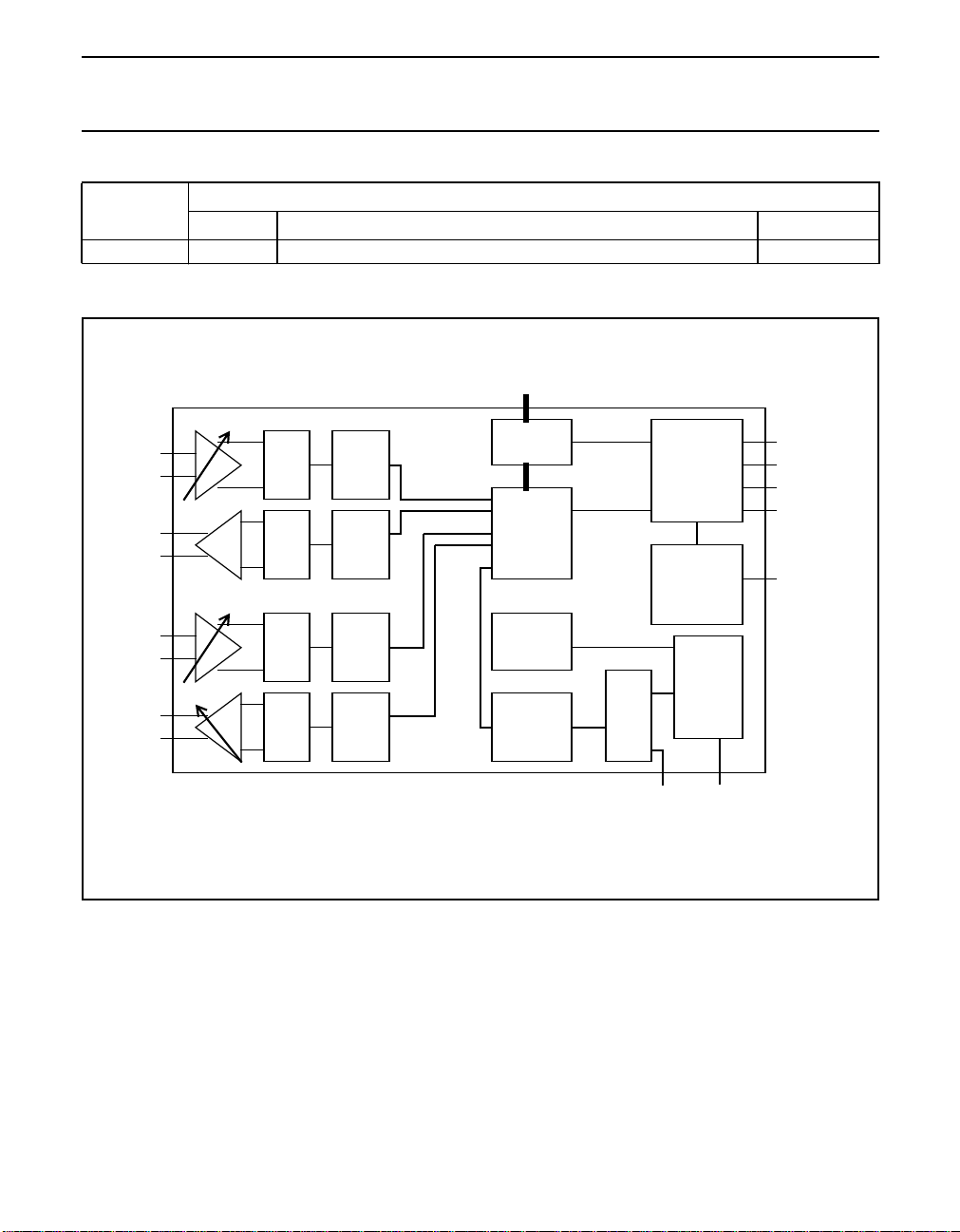
BLOCK DIAGRAM
PACKAGE
IO(n)
TINP
TINN
TOUTP
TOUTN
MICP
MICGND
SKRP
SKRN
1 bit
ADC
4 bit
DAC
1 bit
ADC
4 bit
DAC
down
sample
filter
up
sample
filter
down
sample
filter
up
sample
filter
Digital IO
circuits
data /
control
registers
Voltage
reference
10 bit ADC
Fig.1 Block diagram.
Serial bus
interface
Clock buffers &
sample rate
dividers
multiplexer
AD(n)
touch
screen
interface
SIBDIN
SIBDOUT
SIBSYNC
IRQOUT
SIBCLK
TSPX,TSMX
TSPY,TSMY
2000 Jun 26 3
Page 4

Philips Semiconductors Product specification
Advanced modem/audio analog front-end UCB1300
PINNING
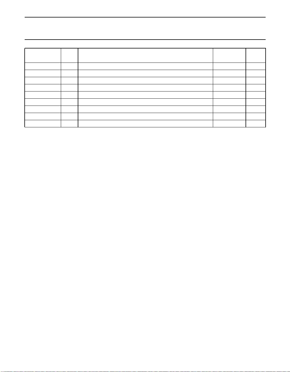
SYMBOL PIN DESCRIPTION
RESET
STATE
IO7 1 general purpose I/O pins input I/O
IO8 2 general purpose I/O pins input I/O
IO9 3 general purpose I/O pins input I/O
ADCSYNC 4 ADC synchronization pulse input - I
V
SSD
5 digital ground - S
n.c 6 not connected - V
SSA2
7 analog speaker driver ground - S
SPKRN 8 negative speaker output Hi-Z O
SPKRP 9 positive speaker output Hi-Z O
V
DDA2
10 analog speaker driver supply - S
TOUTP 11 positive telecom codec output Hi-Z O
TOUTN 12 negative telecom codec output Hi-Z O
TEST 13 test mode protection ‘0’ I
TINN 14 negative telecom codec input Hi-Z I
TINP 15 positive telecom codec input Hi-Z I
VREFBYP 16 external reference voltage input Hi-Z I/O
V
V
DDA1
SSA1
17 analog supply - S
18 analog ground - S
n.c 19 not connected - MICGND 20 microphone ground switch input Hi-Z I
MICP 21 microphone signal input Hi-Z I
AD3 22 analog voltage inputs Hi-Z I
AD2 23 analog voltage inputs Hi-Z I
AD1 24 analog voltage inputs Hi-Z I
AD0 25 analog voltage inputs Hi-Z I
V
SSA3
26 analog touch screen ground - S
TSPY 27 positive Y-plate touch screen Hi-Z I/O
TSMX 28 negative X-plate touch screen Hi-Z I/O
TSMY 29 negative Y-plate touch screen Hi-Z I/O
TSPX 30 positive X-plate touch screen Hi-Z I/O
n.c 31 not connected - V
DDD
32 digital supply - S
IO0 33 general purpose I/O pins input I/O
IO1 34 general purpose I/O pins input I/O
IO2 35 general purpose I/O pins input I/O
IO3 36 general purpose I/O pins input I/O
V
SSD
37 digital ground - S
RESET 38 asynchronous reset input - I
SIBSYNC 39 SIB synchronization input - I
TYPE
C
C
C
C
(2)
A
A
A
A
C
A
A
A
A
A
A
A
A
A
A
A
A
A
C
C
C
C
C
C
(1)
2000 Jun 26 4
Page 5
Philips Semiconductors Product specification
Advanced modem/audio analog front-end UCB1300
SYMBOL PIN DESCRIPTION
SIBDOUT 40 SIB data output ‘1’
RESET
STATE
(6)
SIBCLK 41 SIB serial interface clock − I
SIBDIN 42 SIB data input − I
IRQOUT 43 interrupt output ‘0’ O
TYPE
O
C
C
C
C
(1)
n.c 44 not connected −−
IO4 45 general purpose I/O pins input I/O
IO5 46 general purpose I/O pins input I/O
IO6 47 general purpose I/O pins input I/O
V
DDD
48 digital supply − S
C
C
C
Notes
1. I/OC= CMOS bidirectional; ID= digital input; S = supply; OA= analog output; IC= CMOS input; IA= analog input;
I/OA= analog bidirectional; OC= CMOS output.
2. V
(pins 5 and 37) and V
SSD
(pin 18) are connected internally within the UCB1300.
SSA1
3. SKPRN/SPKRP (pins 8 and 9), TINN/TINP (pins 14 and 15) and TOUTP/TOUTN are differential pairs
4. TEST (pin 13) is connected to an internal pull-down resistor. This pin should be held LOW during normal operation
of the circuit.
5. The ‘not connected’ pins (pins 6, 19, 31 and 44) are reserved for future applications and should be left floating.
6. SIBDOUT reset state is 1 until the SIB bus is running. SIBDOUT will be active once the SIB bus has started.
2000 Jun 26 5
Page 6

Philips Semiconductors Product specification
Advanced modem/audio analog front-end UCB1300
book, full pagewidth
IO7
IO8
IO9
ADCSYNC
V
SSD
n.c.
V
SSA2
SPKRN
SPRKP
V
DDA2
TOUTP
TOUTN
DDD
V
1
2
3
4
5
6
7
8
9
10
11
12
TEST
IO5
IO6
48
47
46
13
14
15
TINP
TINN
n.c.
IO4
45
44
UCB1300
16
17
DDA1VSSA1
V
IRQOUT
43
XXX
18
VREFBYP
SIBCLK
SIBDIN
42
41
19
20
n.c.
MICGND
SIBDOUT
40
21
MICP
RESET
SIBSYNC
39
38
22
23
AD3
AD2
SSD
V
37
24
AD1
36
35
34
33
32
31
30
29
28
27
26
25
MXXxxx
IO3
IO2
IO1
IO0
V
DDD
n.c.
TSPX
TSMY
TSMX
TSPY
V
SSA3
AD0
Fig.2 Pin configuration.
2000 Jun 26 6
Page 7

Philips Semiconductors Product specification
Advanced modem/audio analog front-end UCB1300
FUNCTIONAL DESCRIPTION
The UCB1300 consists of several analog and digital sub-circuits which can be programmed via the Serial Interface Bus
(SIB). This enables the user to set the UCB1300 functionality according to actual application requirements.
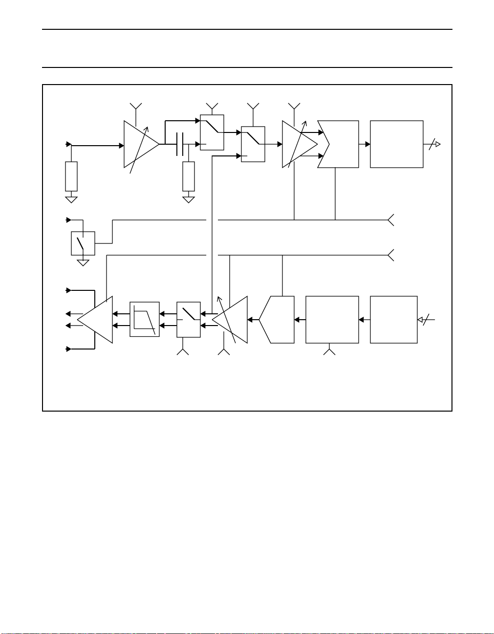
AUDIO CODEC
The audio codec contains an input channel, built up with a 64 timesoversampling sigma delta analog todigital converter
(ADC) with digital decimation filters and a programmable gain microphone preamplifier. The programmable gain
microphone amplifier features a built-in offset cancellation stage, which reduces the distortion of this stage at high gain
settings, caused by the offset voltages of the internal amplifiers or leakage on the board. It can be deactivated (reg13,
bit 13) for improved performance at low gain settings. A general rule is that below a gain setting of 16 (24dB gain) the
offset cancellation circuit will reduce THD and signal bandwidth and should then be deactivated.
The output path consists of a digital up-sample filter, a 64 time oversampling 4-bit digital-to-analog converter (DAC)
circuit followed by a BTL speaker driver, capable of driving a 16 Ω speaker. The output path features a digital
programmable attenuation and a mute function.
The audio codec also incorporates a loopback mode, in which codec output path and the input path are connected in
series.
2000 Jun 26 7
Page 8
Philips Semiconductors Product specification
Advanced modem/audio analog front-end UCB1300
AUD_GAIN[4,3] AUD_OFF_CAN AUD_LOOP AUD_GAIN[2..0]
MICP
MICGND
VCCSPKR
SPKRP
SPKRN
VSSSPKR
AUD_MUTE AUD_ATT[2..0]
Fig.3 Audio codec block diagram.
4-bit DAC
1-bit ADC
DIGITAL
ATTENUATOR
AUD_ATT[4,3]
DIGITAL
DECIMATION
FILTER
AUD_IN_ENA
AUD_OUT_ENA
DIGITAL
NOISE
SHAPER
12
12
The audio sample rate (fsa) is derived from the SIB interface clock pin (SIBCLK) and is programmable through the SIB
interface using AUD_DIV[n]. The audio sample rate is given by the following equation:
2f
×()
f
=
sa
SIBCLK
-------------------------------------------------64 AUD_DIV[n]×()
(7< AUD_DIV[n] < 128)
For example,a serial clock of 9.216 MHz, with a divisorof 12, results inan audio sample rate of 24.0 kHz. Both therising
and the falling edges of SIBCLK are usedin case AUD_DIV[n]is set toan odd number,which demands a50% duty cycle
of SIBCLK to obtain time equidistant sampling.
2000 Jun 26 8
Page 9

Philips Semiconductors Product specification
Advanced modem/audio analog front-end UCB1300
V
DDA1
17
MICP
21
MICGND
20
V
SSA1
18
PASSIVE
UCB1300 UCB1300
V
DDA1
MICGND
17
MICP
21
20
V
SSA1
18
ACTIVE
Fig.4 Possible microphone connections.
The UCB1300audio codec inputpath accepts microphone signalsdirectly, only a DC blocking capacitor isneeded since
the MICP input is biased around 1.4V. The ‘ground’ side of the microphone is either connected to the analog ground
(V
) or to the MICGND pin. The latter will decrease the current consumption of active microphones, since the
SSA1
MICGND pin is made Hi-Z when the audio codec input path is disabled.
The full scale input voltage of the audio input path is programmable in1.5 dB steps by setting the appropriate number in
AUDIO_GAIN[n] in the audio control register A. Using very high gains may require the use of the internal offset
cancellation circuit programmable in reg 13 to avoid clipping in the ADC.
A clipdetection circuit will inform theuser whenever the input voltage exceeds the maximum inputvoltage, since this will
lead to a high distortion. In that case AUD_CLIP_STAT in the audio control register B is set. When ACLIP_RIS_INT is
set, an interrupt is generated on the IRQOUT pin on the rising edge of the clip detect signal. When ACLIP_FAL_INT is
set, an interrupt is generated on the falling edge of the clip detect signal.
The frequency response of the audio codec depends mainly on the selected sample rate, since the bandwidth is limited
in the down and up sampling filters. These digital filters both contain several FIR and IIR low pass filters and a DC
removal filter(high pass filter). A third-order smoothing filter is implemented in the DAC path,between DAC and speaker
driver stage to reduce the spurious frequencies at the speaker outputs.
2000 Jun 26 9
Page 10
Philips Semiconductors Product specification
Advanced modem/audio analog front-end UCB1300
48dB
24dB
0dB
21dB
0dB
24dB
programmed attenuation
48dB 69dB
Fig.5 Analog and digital attenuation settings audio output path.
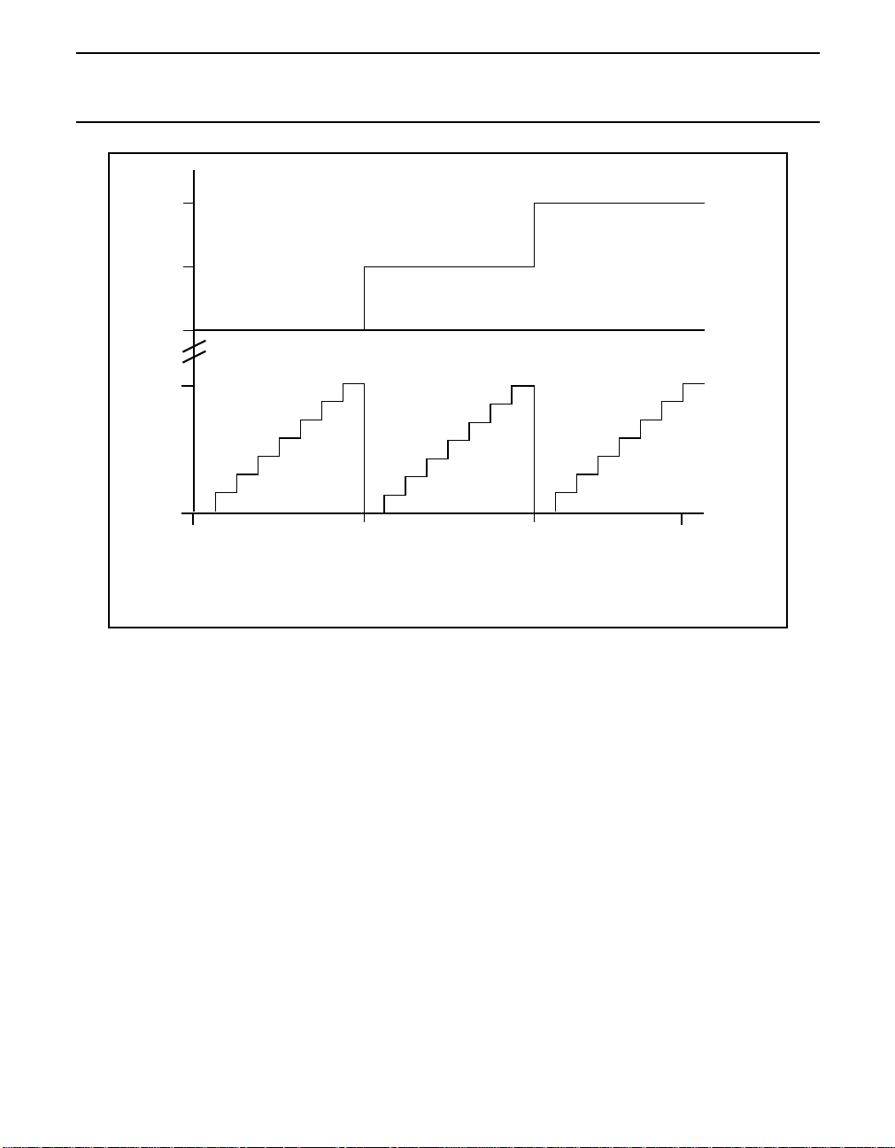
The output level can be attenuated in 3 dB steps down to -69 dB. The first 8 attenuation steps (0 to 21 dB) are
implemented in the analog domain. The digital up sample filter contains a 24 dB and a 48 dB attenuation setting. This
arrangement preservesthe resolution, thus the ‘audio quality’ of the audio output signal for attenuationsettings till 21 dB.
The speaker driver is muted when AUDIO_MUTE in the audio control register B is set. The speaker driver will remain
activated in that case, however no signal is produced by the speaker driver circuit.
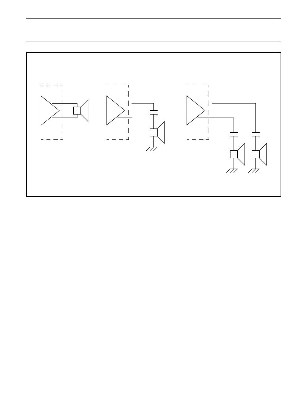
The speaker driver is designed to directly drive a Bridge Tied Load (BTL). This yields the highest output power and this
arrangementdoes notrequire external DC blocking capacitors.The speakerdriver alsoaccepts single-endedconnection
of a speaker, in which case the maximum output power is reduced to a quarter of the BTL situation. Consequently this
way of connecting the speaker to the speaker driver reduces the power consumption of the speaker driver in the
UCB1300 by a factor of 2. Fig.6 shows possible ways to connect a speaker to the driver. Loading the amplifiers with a
capacitive load may cause high frequency oscillations and should be done cautiously.
2000 Jun 26 10
Page 11
Philips Semiconductors Product specification
Advanced modem/audio analog front-end UCB1300
BRIDGE TIED
SPEAKER LOAD
UCB1300 UCB1300 UCB1300
SPKRP
9
+
8
SPKRN
SINGLE-ENDED SPEAKER CONNECTIONS
SPKRP
9
8
SPKRN
SPKRP
9
8
SPKRN
+
+
Fig.6 Possible speaker connections.
The audioinput and outputpath are activated independently.The input pathis enabled when AUDIO_IN_ENAis set, the
output path is enabled when AUD_OUT_ENA is set in the audio control register B. This provides the user the means to
reduce the current consumption of the UCB1300 if one part of the audio codec is not used in the application.
The audio codec has a loopback mode for system test purposes, which is activated when the AUDIO_LOOP bit in the
audio control register B is set. This is an analog loopback which internally connects the output of the audio output path
to the input of the audio input path, (see Fig.3). In this mode the normal microphone input is ignored, but the speaker
driver can be operated normally.
+
2000 Jun 26 11
Page 12
Philips Semiconductors Product specification
Advanced modem/audio analog front-end UCB1300
TELECOM CODEC
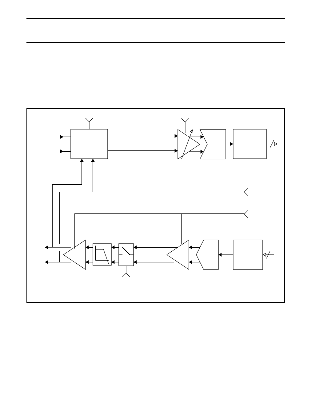
The telecom codec contains an input channel, built up from a 64 times oversampling sigma delta analog-to-digital
converter (ADC) with digital decimation filters, programmable attenuation gain and built-in sidetone suppression circuit.
The output path consist of a digital up-sample filter, a 64 times oversampling 4-bit digital-to-analog converter (DAC)
circuit followed by a differential output driver, capable of directly driving a 600 Ω isolation transformer. The output path
includes a mute function. The telecom codec also incorporates a loopback mode, in which codec output path and the
input path are connected in series.
TOUTP
TOUTN
TINP
TINN
TEL_SIDE_ENA
SIDETONE
SUPPRESSION
CIRCUIT
TEL_MUTE
TEL_ATTATT TEL_GAIN
1-bit ADC
4-bit DAC
DIGITAL
DECIMATION
FILTER
TEL_IN_ENA
TEL_OUT_ENA
DIGITAL
NOISE
SHAPER
14
14
Fig.7 Telecom codec block diagram.
The telecom sample rate (fst) is derived from the SIB interface clock pin (SIBCLK) and is programmable through the SIB
interface. The telecom sample rate is given by the following formula:
2F
×()
f
=
------------------------------------------------- -
st
SIBCLK
64 TEL_DIV[n]×()
(15 < TEL_DIV[n] <128)
For example, a SIBCLK of 9.216 MHz, with a divisor of 40, results in a telecom sample rate of 7.2 kHz. Both the rising
and the falling edges of the SIBCLK are usedin case TEL_DIV[n] is set to an odd number. In that case a 50% duty cycle
of the SIBCLK signal is mandatory to obtain time equidistant sampling.
The input path of the telecom codec has a programmable attenuation gain. It also implements a voice band filter, which
consists ofa digital low pass filter,which is a part of the decimation filter. Therefore the pass band of the voice band filter
2000 Jun 26 12
Page 13

Philips Semiconductors Product specification
Advanced modem/audio analog front-end UCB1300
is determinedby the selectedtelecom codec sample rate.This voice bandfilter is activated bysetting TEL_VOICE_ENA
in the telecom control register B. The resulting telecom input filter curves are given in Fig.38 and Fig.39.
The output section of the telecom codec is designed to interface with a 600 Ω line through an isolation transformer. The
built-in mutefunction is activated byTEL_MUTE in the telecom control register B. The output driver remainsactive in the
mute mode, howeverno output signal is produced. Loading the drivers with a capacitive load may cause high frequency
oscillations and should be done cautiously.
2000 Jun 26 13
Page 14
Philips Semiconductors Product specification
Advanced modem/audio analog front-end UCB1300
TOUCH SCREEN MEASUREMENT MODES
The UCB1300 contains an on-chip interface for a 4 wire resistive touch screen. This interface supports three modes of
touch screen measurements: position, pressure and plate resistance.
POSITION MEASUREMENT
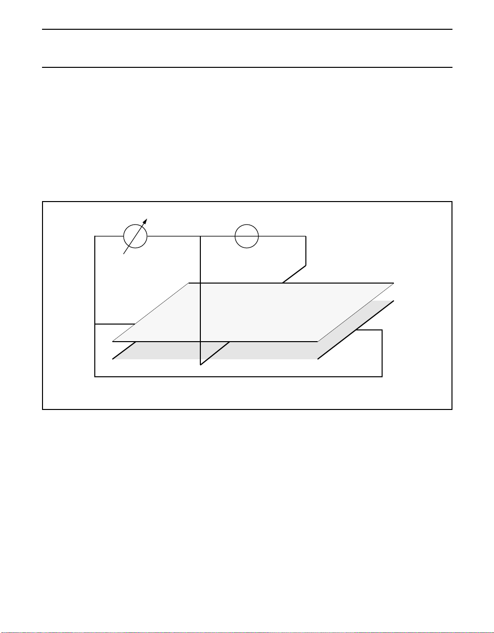
Twoposition measurementsare needed to determine thelocation ofthe pressedspot. Firstan Xmeasurement, secondly
a Y measurement. The Xplate is biasedduring the X position measurement of theX plate andthe voltage onone or both
Y terminals (TSPY, TSMY) measured. The circuit can then be represented by a potentiometer, with the TSPY and/or
TSMY electrode being the ‘wiper’. The measured voltage on the TSPY/TSMY terminal is proportional to the X position
of the pressed spot of the touch screen.
Vposition
Vtscbias
tspx
tsmy
tspy
tsmx
Fig.8 Touch screen setup for position measurement.
In the Y position mode the X plate and Y plate terminals are interchanged, thus the Y plate is biased while the voltage
on the TSPX and/or TSMX terminal is measured.
2000 Jun 26 14
Page 15
Philips Semiconductors Product specification
Advanced modem/audio analog front-end UCB1300
PRESSURE MEASUREMENT
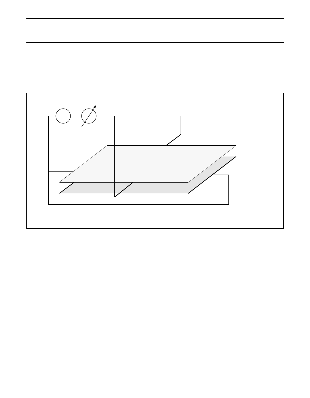
The pressure used to press the touch screen can be determined. In fact, the contact resistance between the X and Y
plate is measured, which is a good indication of the size of the pressed spot and the applied pressure. A soft stylus, e.g.
a finger, leads to a rather large contact area between the two plates when a large pressure is applied. A hard stylus, e.g.
a pen, leads to less variation in measured contact resistance since the contact area is rather small.
Vtscbias
ipressure
tspx
tsmy
tspy
tsmx
Fig.9 Touch screen setup for pressure measurement.
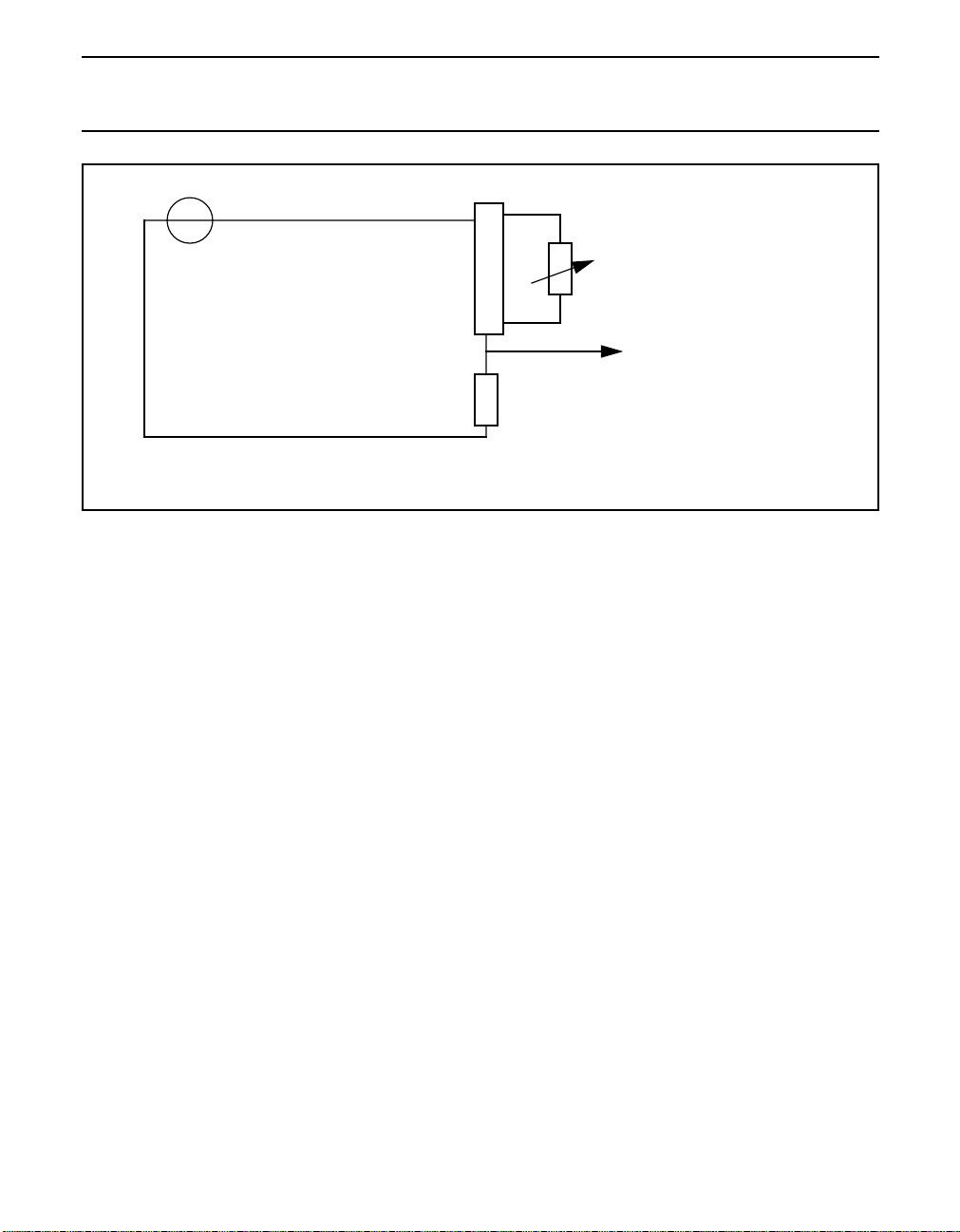
One plate is biased at one or both terminals during this pressure measurement, whereas the other plate is grounded,
again on one or both terminals. The current flowing through the touch screen is a direct indication for the resistance
between both plates. A compensation for the series resistance, formed by the touch screen plates itself will improve the
accuracy ofthis measurement. The measurement is done with a resistive voltage divider. The internalresistor should be
taken into account to evaluate the settling time of the pressure measurement given the board capacitors connected to
the ADC tap point in pressure mode.
2000 Jun 26 15
Page 16
Philips Semiconductors Product specification
Advanced modem/audio analog front-end UCB1300
Vtscbias
Measured resistor
Switch matrix
To ADC
Internal resistor (about 1kΩ)
Fig.10 Pressure measurement scheme.
2000 Jun 26 16
Page 17

Philips Semiconductors Product specification
Advanced modem/audio analog front-end UCB1300
PLATE RESISTANCE MEASUREMENT
Theplate resistance of a touchscreen typicallyvaries alot due to processing spread.Knowing theactual plateresistance
makes it possible to compensate for the plate resistance effects in pressure resistance measurements. The plate
resistance decreases when two or more spots on the touch screen are pressed.In that case, a part of one plate, e.g. the
X plate, is shorted by the other plate, which decreases the actual plate resistance
Vtscbias
iplate
tspx
tsmy
tspy
tsmx
Fig.11 Touch screen setup for plate resistance.
The plate resistance measurement is executed in the same way as the pressure resistance measurement. In this case
only one of the two plates is biased and the other plate is kept floating. The current through the connected plate is again
a direct indication of the connected resistance.
2000 Jun 26 17
Page 18
Philips Semiconductors Product specification
Advanced modem/audio analog front-end UCB1300
TOUCH SCREEN INTERFACE
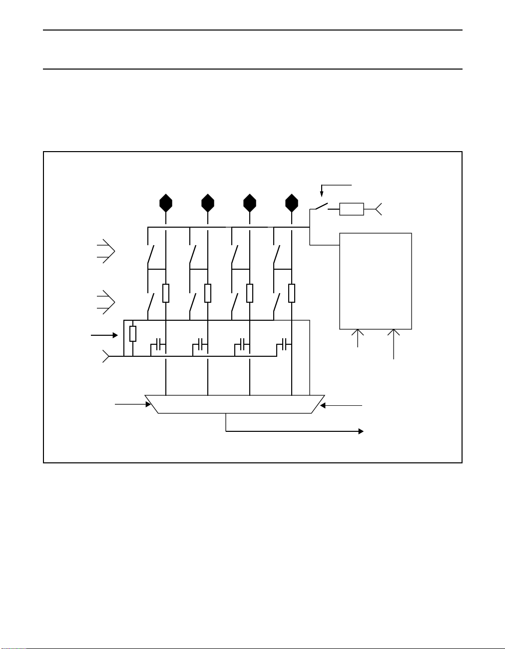
The UCB1300 contains a universal resistive touch screen interface for 4-wire resistive touch screen, capable of
performing position, pressure and plate resistance measurements. In addition, the touch screen can be programmed to
generate interrupts when the touch screen is pressed. The last mode is also active when the UCB1300 is set in the
stand-by mode.
ts..power
ts..ground
tsc_mode
(pressure)
vssa3
adc_input[2:0]
tspx
tsmx
tspy
tsmy
1kΩ
analog mux
Fig.12 Block diagram of the touch screen interface.
tsc_mode (interrupt)
vdda1
touch screen
bias voltage
vssa1
tsc_bias_ena
Current sense input
tsc_mode_sel
to adc input
The touch screen interface connects to the touch screen by four wires: TSPX, TSMX, TSPY and TSMY. Each of these
pinscan be programmedto befloating, powered or grounded inthe touchscreen switch matrix.The settingof each touch
screen pin is programmable through the touch screen control register. Possible conflicting settings (grounding and
powering of a touch screen pin at the same time) are detected by the UCB1300. In that case, the touch screen pin will
be grounded.
In position mode, opening the TS..gnd switch can take a long time. To avoid unpredictable delays after changing the
plates configuration, the touch screen interface should be programmed to pressure mode for the duration 1 SIB frame
before resuming a position measurement.
TheUCB1300’s internalvoltage reference (V
the touch screen biasing independent of supply voltage and temperature variations. Four low pass filters, one on each
touch screen terminal, are built in to minimize the noise coupled from the LCD into the touch screen signals. An LCD
typically generateslarge noise glitches on thetouch screen, since they are closely coupled. The influence of the glitches
2000 Jun 26 18
)is usedas reference voltage for the touch screenbias circuit.This makes
ref
Page 19
Philips Semiconductors Product specification
Advanced modem/audio analog front-end UCB1300
can neverthelessbe minimized by performing measurementswhen the LCD is quiet.This can be done bysynchronizing
the measurement and the video driver with the ADCSYNC pin.
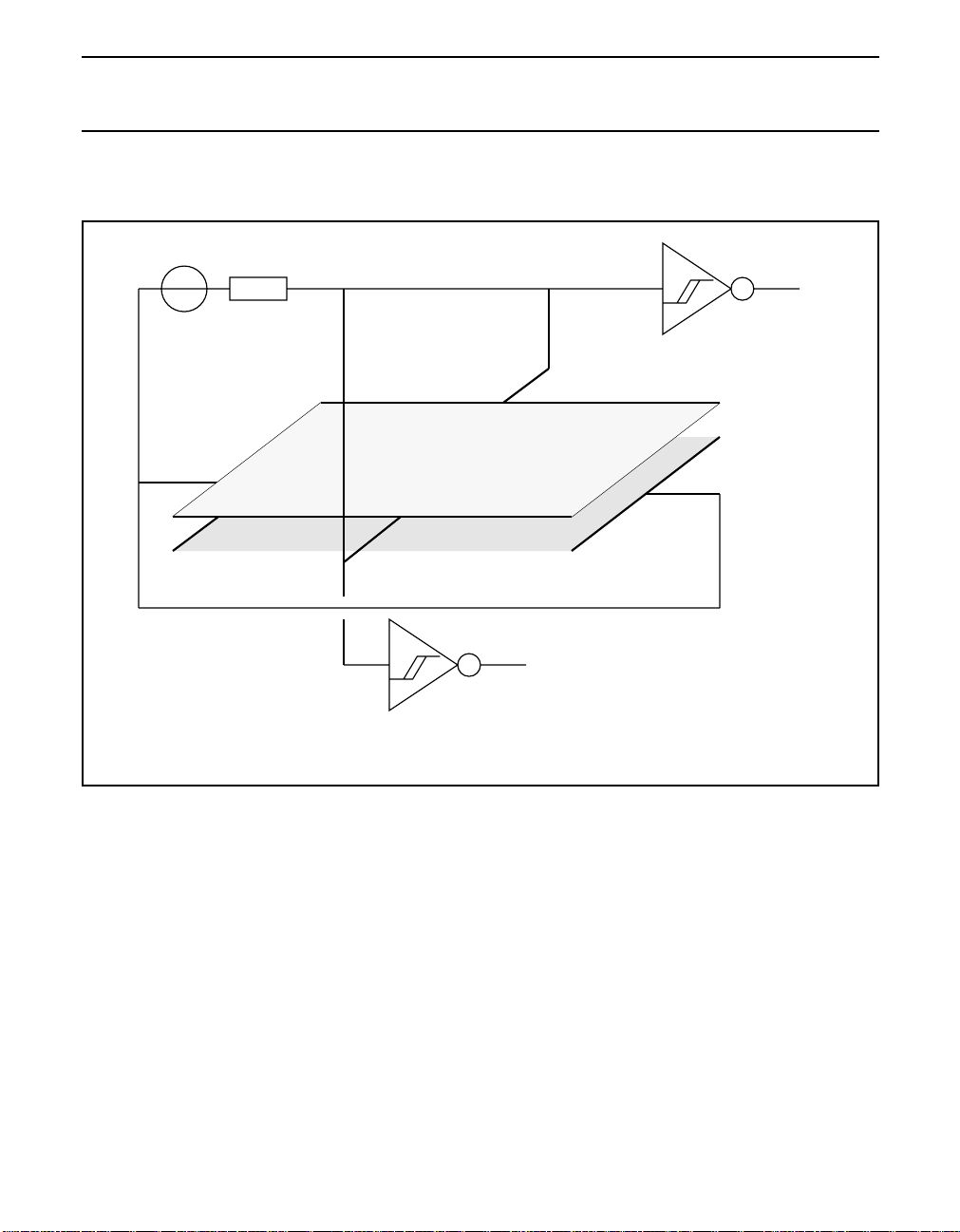
Vdda
tsmy
Rint
schmitt trigger
tspx
tspy
tsmx
schmitt trigger
Fig.13 Touch screen setup for interrupt detection.
In addition to the measurements mentioned above, the touch screen can also act as an interrupt source. In this mode
the X plate of the touch screen has to be powered and the Y plate has to be grounded. In this case the touch screen is
not biased by the active touch screen bias circuit, but by a resistor to V
screen and the UCB1300 does not consume power unless the touch screen is touched. The voltage on the X plate
terminals drops if the screen is pressed. This voltage drop is detected by Schmitt-trigger circuits, of which the outputs
are connected to the interrupt control block. A touch screen interrupt is generated either when the touch screen is
pressed (falling edge enabled) or when the touchscreen is released (rising edge enabled).It can be used to activate the
system around the UCB1300 to start a touch screen read-out sequence. The internal Schmitt-trigger circuits are
connected to the TSPX and TSMX signals after the built-in low pass filters. This reduces the number of spurious
interrupts, due to the coupling between the LCD screen and the touch screen sensors.
Each of thefour touch screen signals can be selected as input for the built-in 10-bit ADC, which is used to determine the
voltage on the selected touch screen pin. The flexible switch matrix and the multi-functional touch screen bias circuit
enables the user of the UCB1300 to set each desired touch screen configuration.
2000 Jun 26 19
. This configuration simply biases the touch
DDA1
Page 20
Philips Semiconductors Product specification
Advanced modem/audio analog front-end UCB1300
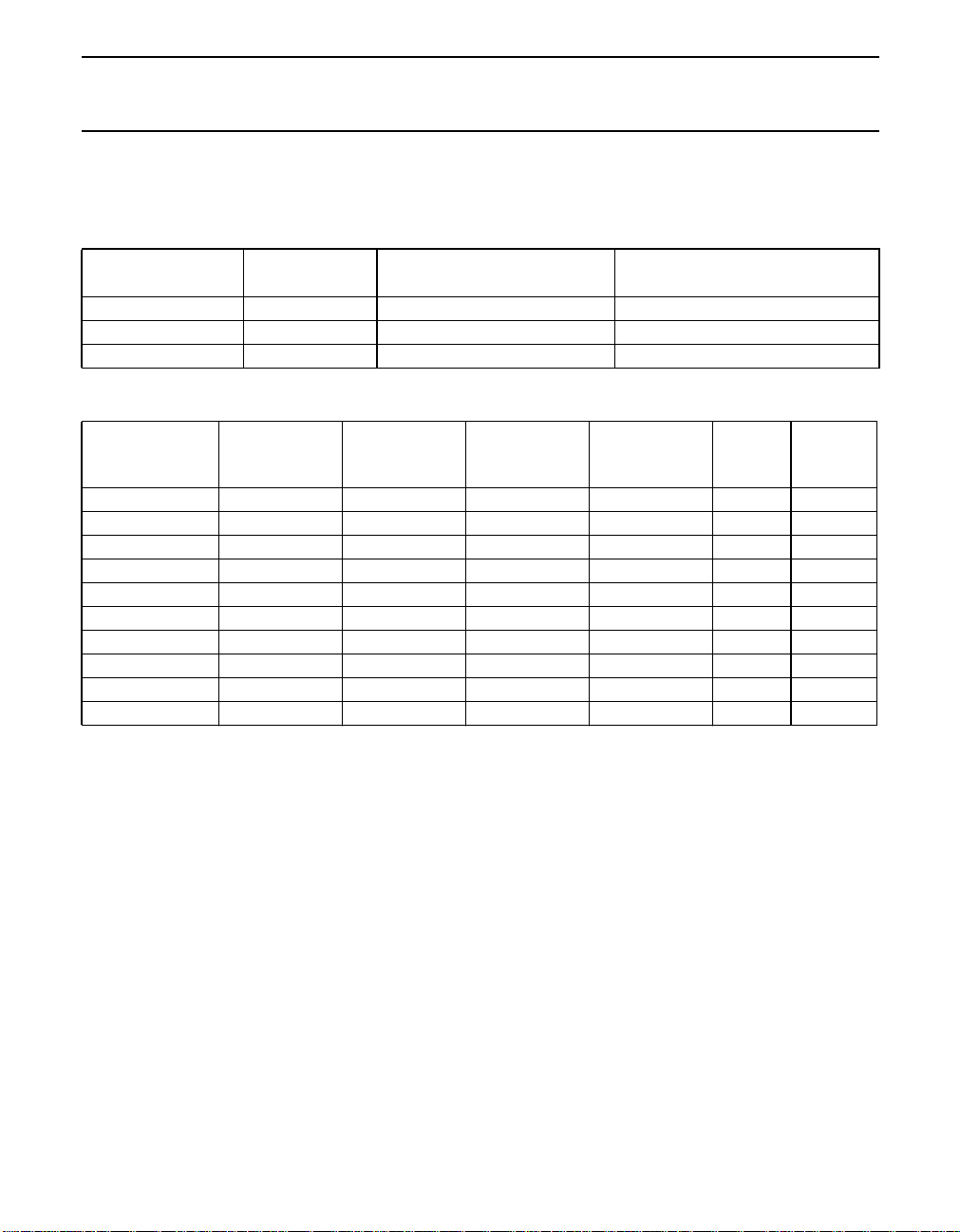
The setting of the touch screen bias circuit and the ADC input multiplexer is determined by the setting of TSC_MOD[n]
in the touch screen control register according the following table.
TOUCH SCREEN MODE SELECTION
TSC_MODE[N] SELECTED BITS
00 interrupt resistor to V
TOUCH SCREEN BIAS
SOURCE
DDA1
01 pressure touch screen bias circuit touch screen current monitor
1X position touch screen bias circuit defined by ADC_INPUT[n]
SUMMARY OF TOUCH SCREEN MODES; note 1
TOUCHSCREEN
MEASUREMENT
X position powered
Y position ADC_INPUT[n] ADC_INPUT[n] powered
pressure - 1 powered
TSPX TSMX TSPY TSMY
(2)
(2)
grounded
powered
(2)
(2)
ADC_INPUT[n] ADC_INPUT[n] position enabled
(2)
grounded
(2)
pressure - 2 powered floating grounded floating pressure enabled
pressure - 3 floating grounded powered floating pressure enabled
pressure - 4 floating powered floating grounded pressure enabled
pressure - 5 grounded floating floating powered pressure enabled
X-plate resistance powered
(2)
grounded
Y-plate resistance floating floating powered
(2)
floating floating pressure enabled
(2)
interrupt powered powered grounded grounded interrupt disabled
Notes
1. Control register address 9 is used for touch screen mode selection.
2. The powered and grounded touch screen pins may be interchanged.
3. In this mode, the touch screen bias must be disabled by the user to prevent false interrupts.
ADC MULTIPLEXER SETTING
(TOUCH SCREEN INPUTS)
defined by ADC_INPUT[n]
TOUCH
SCREEN
MODE
grounded
grounded
grounded
(2)
(2)
(2)
position enabled
pressure enabled
pressure enabled
TOUCH
SCREEN
BIAS
(3)
2000 Jun 26 20
Page 21
Philips Semiconductors Product specification
Advanced modem/audio analog front-end UCB1300
10-BIT ADC
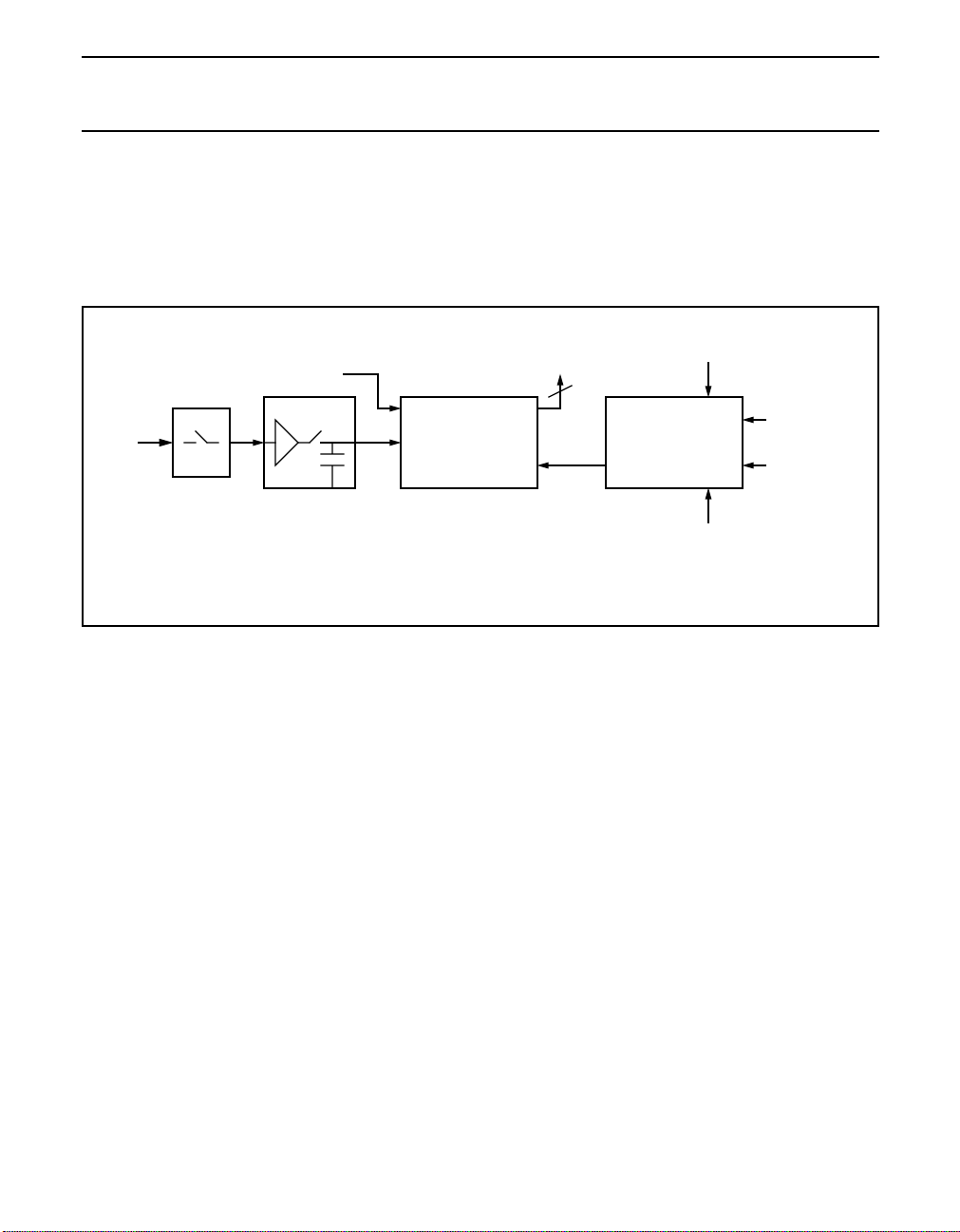
The UCB1300 includes a 10-bit successive approximation analog-to-digital converter (ADC) with built-in track and hold
circuit and an analog multiplexer to select one of the 4 analog inputs (AD0 - AD3), the 4 touch screen inputs (TSPX,
TSMX, TSPY, TSMY) or the pressure output of the touch screen bias circuit. The ADC is used to read-out the touch
screen inputs and it measures the voltage on the four analog high voltage inputs AD0 - AD3. The analog multiplexer
contains 4 resistive dividers to attenuate the high voltage on the AD0 - AD3 inputs to the ADC input range.
internal reference
mux
9 to 1
The ADC is controlled completely through the SIB interface, but the UCB1300 contains internal logic to ease the control
of the ADC and to minimize the number of SIB frame read/write actions.
A complete ADC control sequence analog to digital conversion consists of several phases. Firstly, the ADC has to be
enabled; secondly, the input selector must be set to the proper input; thirdly, the ADC conversion has to be started; and
finally, the ADC result has to be read from register 11.
The ADC is activated by setting ADC_ENA in register 10. The ADC circuit, including the track and hold circuit does not
consume any power aslong as thisbit is reset. The analoginput multiplexer iscontrolled by ADC_INPUT[n] and theADC
isactually startedwith theADC_START bit. When TSPX and TSMX are in theinterrupt mode,the ADCcannot bestarted,
even to measure AD0-3.
The UCB1300 has two different modes to start the ADC conversion, which are selected by the ADC_SYNC_ENA bit.
The default mode is the non-synchronization mode, in which the conversion is started directly with a 0-to-1 transition of
ADC_START. Secondly the ADC is started at a rising edge of the signal applied to the ADCSYNC pin if
ADC_SYNC_ENA isset. Activating the ADC whilekeeping the start logic inthe started state (ADC_START =1) will lead
to unpredictable behavior andthe value ofthe ADCdata register willnot be meaningful.Always activatea start sequence
for each acquisition (0-to-1 transition on the internal ADC_START signal).
The internal track and hold circuit requires a certain settling time to track the input signal correctly. This can be ensured
from the software bywriting first aSIB frame with the ADCmultiplexer setting beforethe SIB frame with theADC_START
command is transferred. TheUCB1300 ADC start/stop logic will detect whether the ADC input multiplexer is changed in
the same SIB frame as the ADC start command is given. In that case, it will delay the actual start of the ADC circuit to
ensure that the track and hold settling time requirements are met. This leads to the following two timing diagrams:
track&hold
10-bit ADC
Fig.14 Block diagram of the 10-bit ADC circuit.
to control reg 11
10
adcsync
ADC start
stop logic
adc_sync_ena
adc start
sync
enable
2000 Jun 26 21
Page 22
Philips Semiconductors Product specification
Advanced modem/audio analog front-end UCB1300
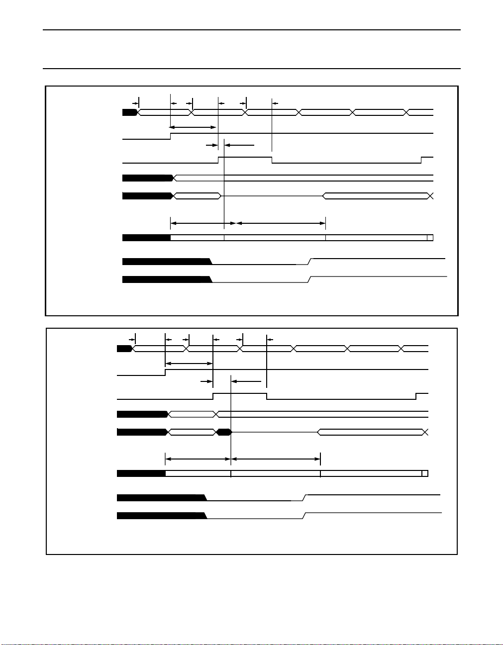
‘SIB frame’
adc_ena (internal)
adc_start (internal)
adc_input_selection
‘adc start state’
‘adc state’
adc_dat_valid
adc_data
Fig.15 ADC timing sequence, non ADC sync mode, no changing ADC input multiplexer settings.
‘SIB frame’
adc_ena (internal)
tsibwrite tsibwrite
set adc_ena:1 set adc_start:1 set adc_start:0 read adc result
tsibwrite tsibwrite
set adc_ena:1 set adc_start:1 set adc_start:0 read adc result
tsibwrite
tadcena
tsamdel1
wait for start wait for start
ttrckmin
tracking conversion tracking
tsibwrite
tadcena
tadcconv
tsamdel2
adc_start (internal)
adc_input_selection
‘adc start state’
‘adc state’
wait for start wait for start
ttrckmin
tracking conversion tracking
tadcconv
adc_dat_valid
adc_data
Fig.16 ADC timing sequence, non ADC sync mode, changing ADC input multiplexer settings.
The ADCtiming diagrams indicate thatin the non-ADC syncmode the ADC resultcan be read in the SIB frame following
the SIB frame with the ADC start command, if the ADC multiplexer setting is not changed. If the ADC input multiplexer
setting is changed, the ADC result can be read in the second SIB frame following the SIB frame with the ADC start
command.
2000 Jun 26 22
Page 23
Philips Semiconductors Product specification
Advanced modem/audio analog front-end UCB1300
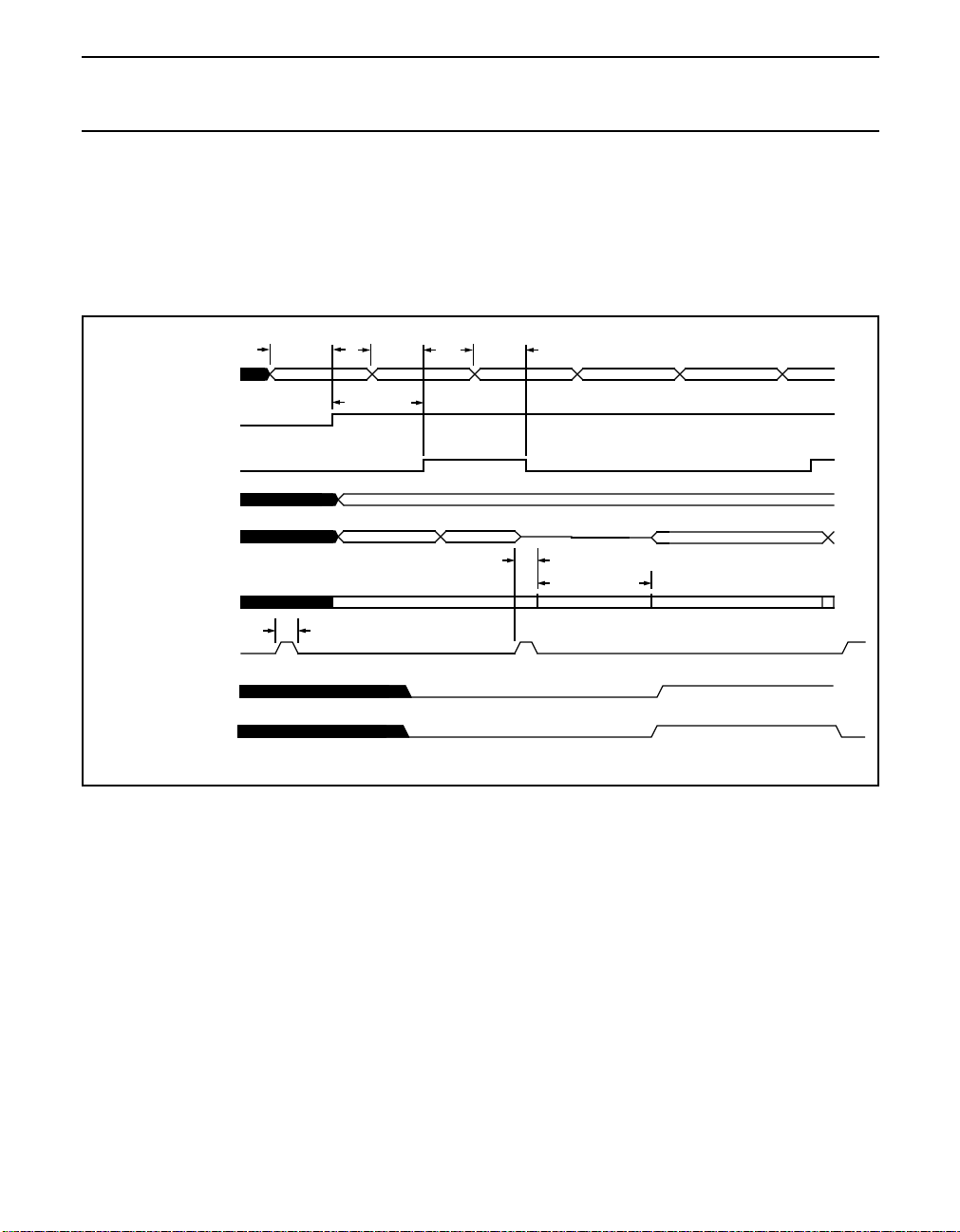
The second ADC start mode gives the opportunity to start the ADC at the rising edge of the signal connected to the
ADCSYNC pin. The 0-to-1 transition of the ADC_START bit will arm the ADC, such that it will start in the first detected
risingedge ofthe ADCSYNCsignal. Alsoin thismode, theinternal start/stoplogic willdetect whether the ADC multiplexer
settings are changed simultaneously with the ADC start bit and it will add a delay to ensure sufficient setting time for the
internal track and hold circuit. A rising edge of the signal connected to the ADCSYNC pin occurring during this tracking
time is ignored; the ADC conversion is started on the first rising edge detected after this delay time. This leads to the
following two timing diagrams of the ADC conversion.
‘SIB frame’
adc_ena (internal)
adc_start (internal)
adc_input_selection
‘adc start state’
‘adc state’
adc_sync
adc_dat_valid
adc_data
Fig.17 ADC timing sequence, ADC sync mode, no changing ADC input multiplexer settings.
tsibwrite
set adc_ena:1
thadcsync
tsibwrite
set adc_start:1 set adc_start:0 read reg:11
tadcena
wait for start
tracking
tsibwrite
wait for sync wait for start
tadcsam3
tadcconv
conversion tracking
2000 Jun 26 23
Page 24
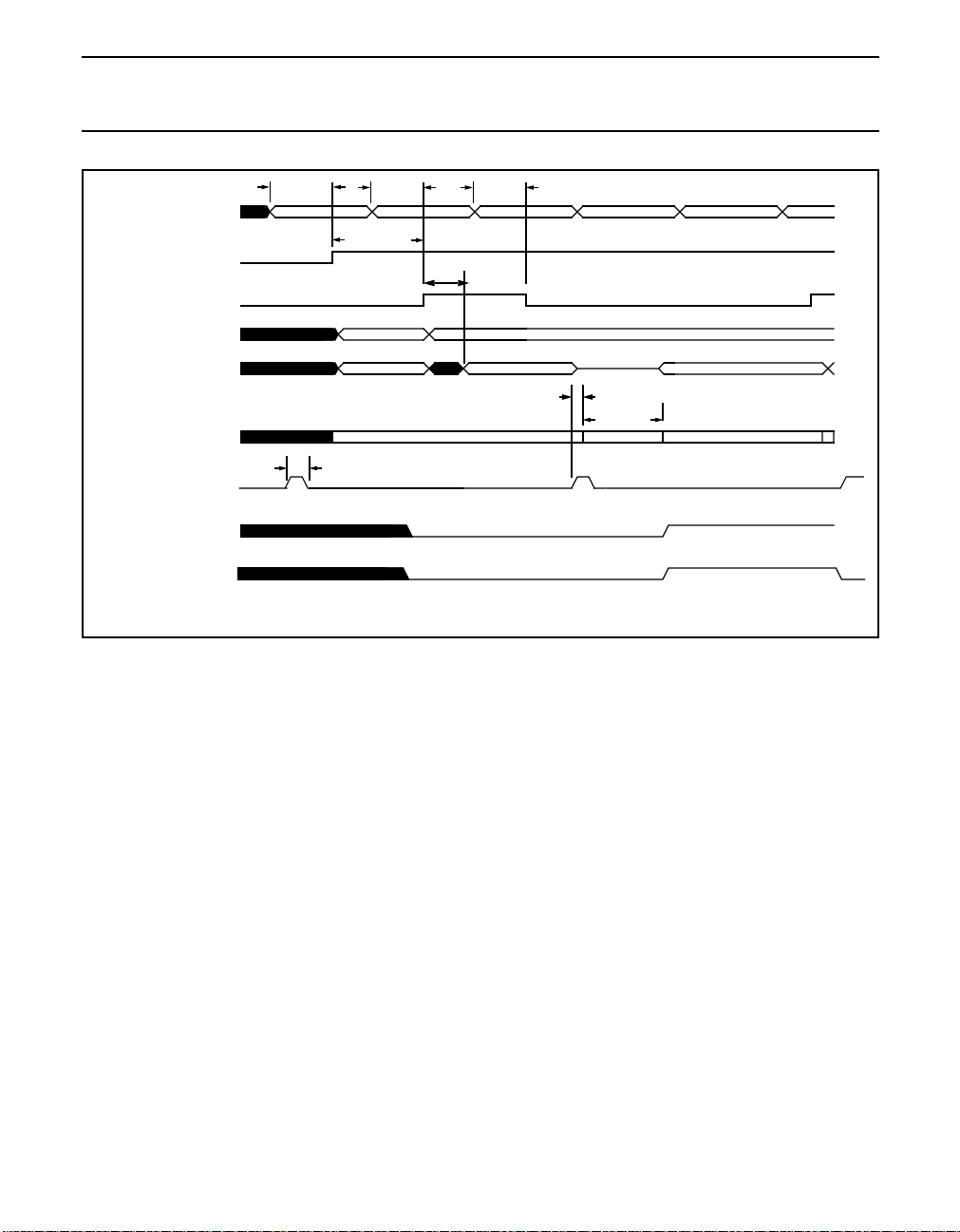
Philips Semiconductors Product specification
Advanced modem/audio analog front-end UCB1300
tsibwrite
set adc_start:1 set adc_start:0 read reg:11
tadcena
‘SIB frame’
tsibwrite tsibwrite
set adc_ena:1
adc_ena (internal)
ttrckmin
adc_start (internal)
adc_input_selection
‘adc start state’
‘adc state’
wait for start
tracking conversion tracking
thadcsync
wait for sync wait for start
tadcsam3
tadcconv
adc_sync
adc_dat_valid
adc_data
Fig.18 ADC timing sequence, ADC sync mode, changing ADC input multiplexer settings.
TheADC sync modeis particularlyuseful when the internal ADChas tobe synchronized to the externalsystem. Typically
it is used to synchronize the read-out of the touch screen to the driving of the LCD screen, which is normally placed
beneath the touch screen. Many spikes and a lot of 'noise' are superimposed on the touch screen signals, due to the
close coupling of the touch screen and the LCD.
The result of the conversion is stored in register 11 of the SIB interface, after the completion of the conversion. An
interrupt may be generated whenever a conversion is completed (ADC_FLA_INT and/or ADC_RIS_INT bits in
register 2 and 3) to ease the synchronization between the UCB1300 and the system controller. The ADC result is reset
to 0x000, whenever the ADC is started or armed till the ADC conversion is completed. ADC_DAT_VAL in the SIB
register 11 indicates the status of the ADC; it equals '0' when an ADC sequence is started, which implies that the ADC
result is not valid and it equals '1' when the ADC conversion is completed and the result is stored in the SIB register 11.
2000 Jun 26 24
Page 25
Philips Semiconductors Product specification
Advanced modem/audio analog front-end UCB1300
AD[n]
adc
input
MUX
ADC_INPUT[n]
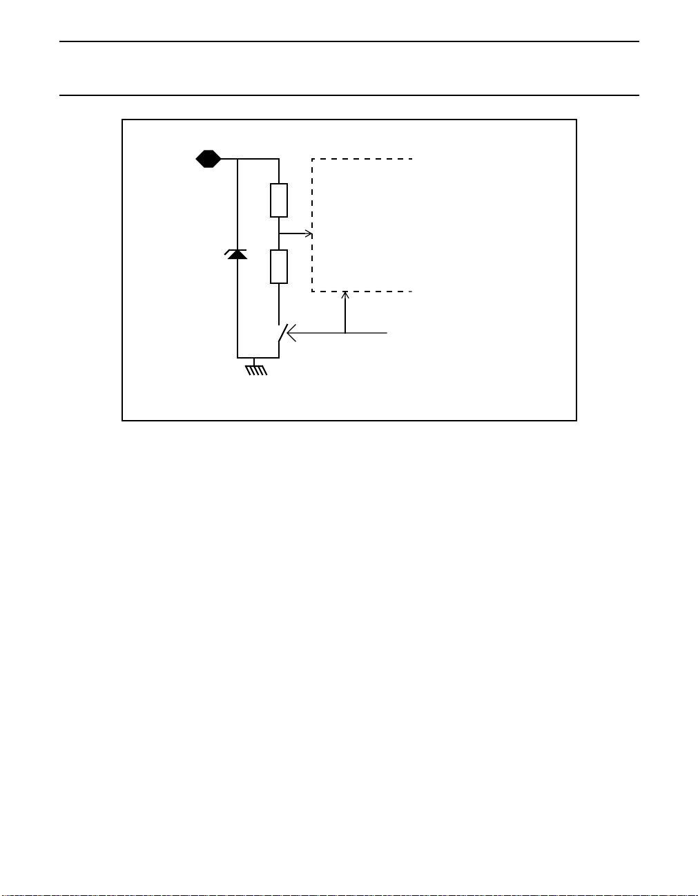
Fig.19 Block diagram of resistive dividers AD0 - AD3.
The applied voltage on the four analog inputs of the UCB1300 (AD0 - AD3) is attenuated before it is applied to the ADC
input multiplexer using on-chip resistive dividers.These high voltage inputs are optimized to handle voltages larger than
the applied supply voltage. The built-in resistive voltage dividers are only activated if the corresponding analog input is
selected. The resistive dividers are made floating when the input is not selected by the ADC input multiplexer, such that
the input leakage ofthese high voltageanalog pinsis minimized. Thismakes these analog inputs verysuitable to monitor
battery voltages.
2000 Jun 26 25
Page 26
Philips Semiconductors Product specification
Advanced modem/audio analog front-end UCB1300
ON-CHIP REFERENCE CIRCUIT
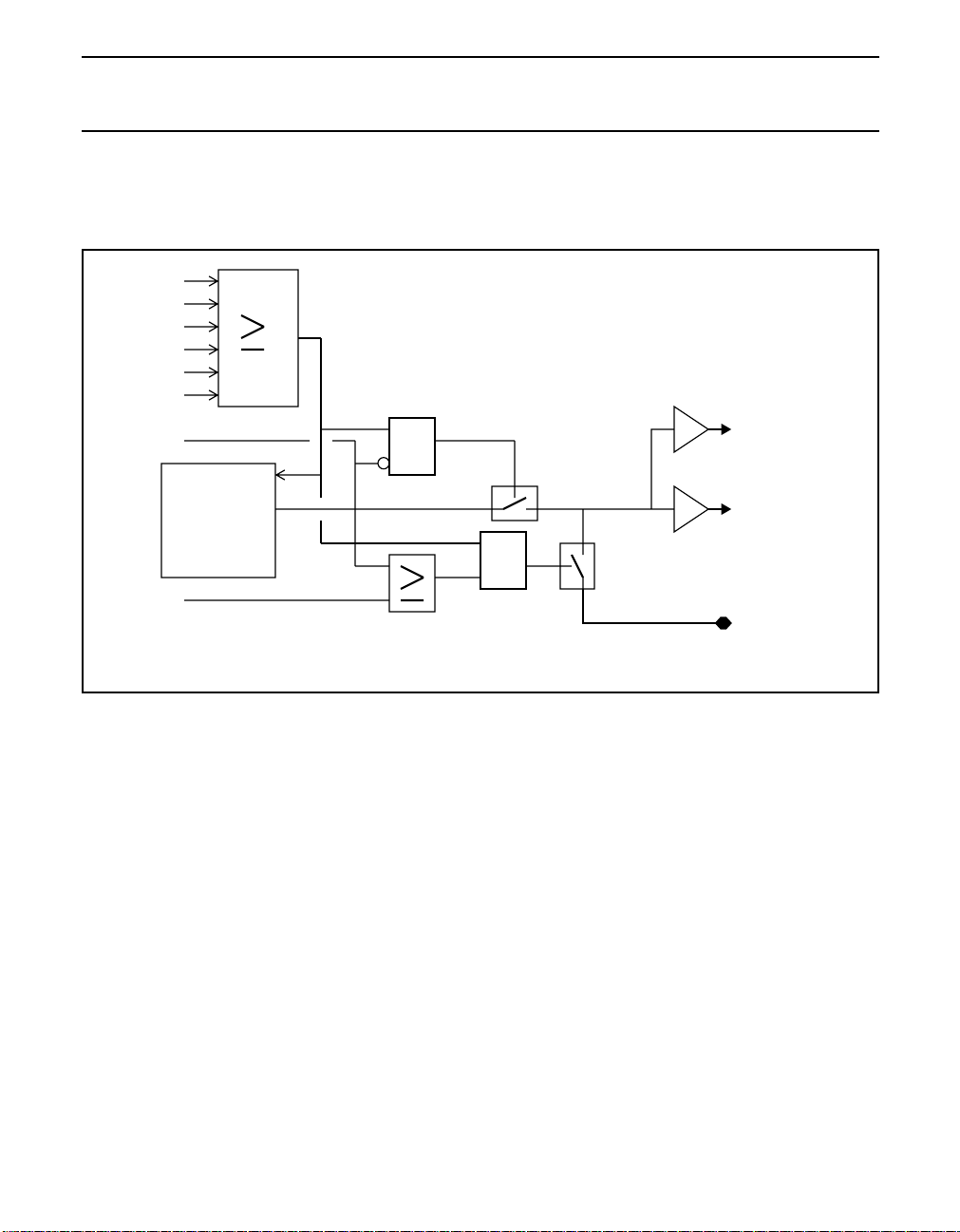
The UCB1300 containsan on-chip reference voltage source, which generates the reference voltages for the 10-bit ADC
and the virtual analog ground. Alternatively the UCB1300 can be driven from an external reference voltage source.
aud_in_ena
aud_out_ena
tel_in_ena
tel_out_ena
tsc_bias_ena
adc_en
internal
ext_vref_ena
vrefbyp_con
internal
bandgap
reference
voltage
circuitry
&
ena
Vbg
&
analog
ground
internal
ADC
reference
vrefbyp
Fig.20 Block diagram of the reference circuit.
Theinternal reference voltage is connectedto theVREFBYP pin, where an externalcapacitor couldbe connected to filter
this reference voltage, if VREF_CON (register 10) is set. THIS IS NOT RECOMMENDED since the internal impedance
ofthe reference (several100 MΩ) will besensitive toboard leakage and the turnon time constant will bevery long.When
choosing a capacitor, the internal impedance (around 50 kΩ) should be taken into account.
An externalvoltage reference connectedto the VREFBYP pinis used asvoltage reference by theUCB1300 circuit, ifthe
EXT_REF_ENA bit (register 10) is set. Two bits in the ADC control register determine the mode of operation of this
reference voltage circuit. VREFBYP_CON connects the internal reference voltage to the VREFBYP pin, while
EXT_VREF_ENA disables the internal reference voltage and switches the UCB1300 into the external voltage reference
mode.
2000 Jun 26 26
Page 27
Philips Semiconductors Product specification
Advanced modem/audio analog front-end UCB1300
SERIAL INTERFACE BUS
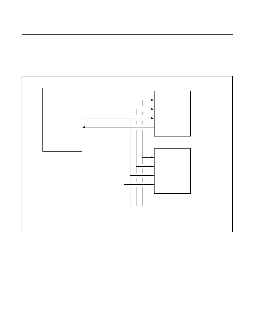
The UCB1300 Serial Interface Bus (SIB) is compatible with industry standard serial ports and devices, and is designed
to connect directly to a system controller. The SIB protocol allows one or more slave devices to be connected to the
system controller. The data transfer is always synchronous and it is frame based. The SIB interface consists of four
signals: SIBDIN, SIBDOUT, SIBCLK and SIBSYNC.
SIB MASTER
sibclk
sibsync
sibdout
sibdin
TO OTHER SIB SLAVES
Fig.21 Typical connection between the UCB1300 and the system controller.
UCB1300
sibclk
sibsync
sibdin
sibdout
SIB SLAVE 2
sibclk
sibsync
sibdin
sibdout
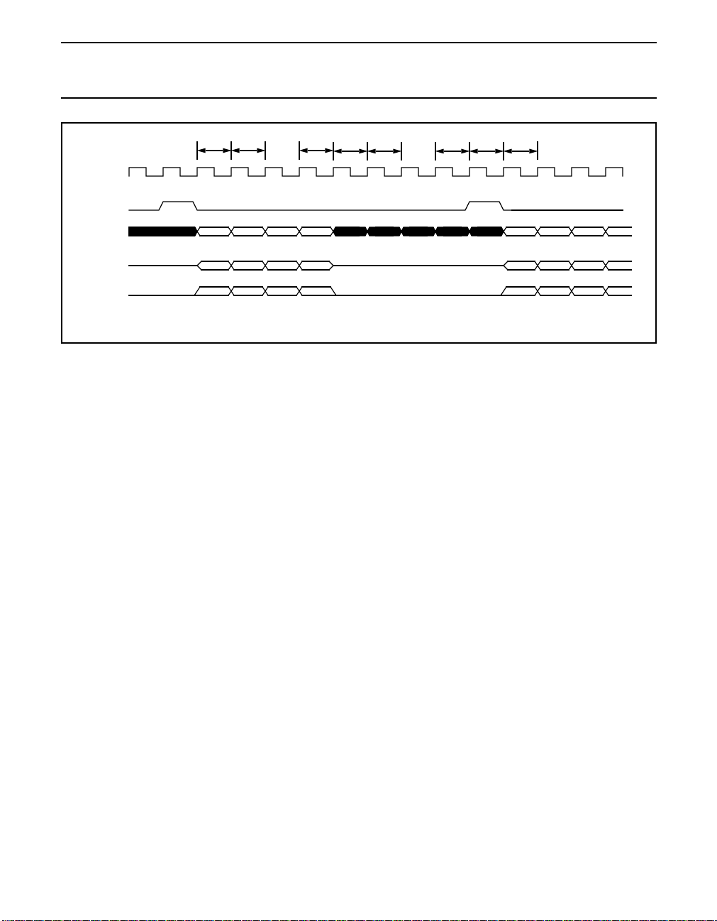
Each SIB frame consists of at least 64clock cycles. Typically128 bits areused, divided into2 sub framesof 64 bitseach.
The first word (thebits 0 to63) is read and/or writtenby the UCB1300,the remaining bitsmay be used for communication
between thesystem controller andanother slave device. TheSIBDOUT pin ofthe UCB1300 is 3-statedfor the bit64 and
higher in the SIB frame to prevent bus conflicts with other slave devices. However, when SIB_ZERO (control register 1)
is set, the SIBDOUT pin is forced to zero from bit 64 onwards to prevent the SIBDOUT line from floating. This feature is
needed when the UCB1300 is the only slave device connected to the bus.
The UCB1300 always samples incoming data on the SIBDIN pin on the falling edge of SIBCLK and it outputs data on
the SIBDOUT pin on the rising edge ofthe SIBCLK. Thestart of anew SIB frameis indicated bya pulse onthe SIBSYNC
line just before the start of this new SIB frame.
2000 Jun 26 27
Page 28
Philips Semiconductors Product specification
Advanced modem/audio analog front-end UCB1300
sibclk
sibsync
sibdin
sibdout #1
sibdout #2
bit 0 bit 1 bit 63
bit 64
bit 65
bit 126 bit 127
bit 0
Fig.22 Serial data transmission of the UCB1300
The applied clock signal to the SIBCLK pin is used as clock signal inside the UCB1300; all internal clock signals are
derived from that. It is required that the SIBCLK signal is applied if one or more analog or digital functions are activated
in the UCB1300; only the interrupt controller is implemented asynchronously. SIBCLK may be stopped when all digital
and analog functions are disabled; in that case the lowest possible power consumption is met. The SIBCLK should not
be stopped during a SIB frame, but only at the end of the SIB-frame, to ensure that all analog and digital functions are
stopped properly.
Note: The interrupt controller is still active, due to its asynchronous implementation. Therefore, the UCB1300 can still
generate interrupts to the system controller, when the SIBCLK is stopped.
The generation of the audio and telecom sample clocks requires that the SIBCLK signal is symmetrical: a
non-symmetrical SIBCLK will leadto non-equidistant sample moments, when an odd frequency divisor isset in either of
the audio or telecom control registers.
2000 Jun 26 28
Page 29
Philips Semiconductors Product specification
Advanced modem/audio analog front-end UCB1300
SIB DATA FORMAT
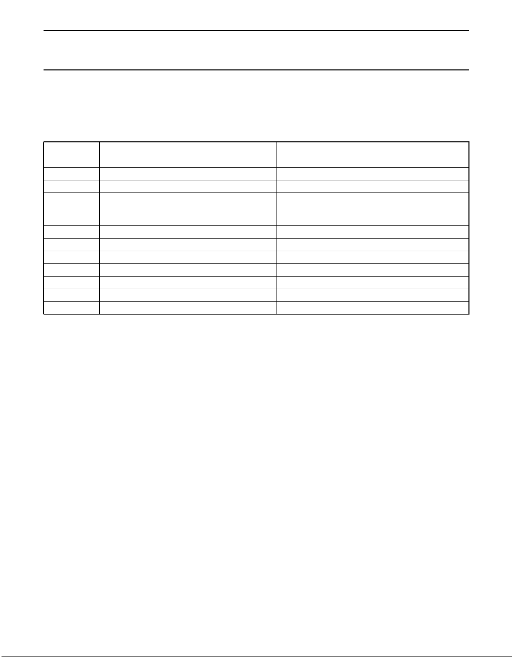
Thefirst 64bits in the SIB-frame are read andwritten bythe UCB1300.They containaudio andtelecom codecdata fields,
several control bits, and a control register data field, as defined in table below.
SIB DATA FORMATS
SIB FRAME
BIT
0 - 11 audio input path data (12 bits); bit 0 = MSB audio output path data (12 bits); bit 0 = MSB
12 - 16 not read but reserved fixed ‘0’
17 - 20 control register address (4 bits); bit 17 = MSB control register address (4 bits); bit 17 = MSB; is a
21 write bit (write 1) fixed ‘0’
22 - 29 not read but reserved fixed ‘0’
30 audio valid sample flag audio valid flag
31 telecom valid sample flag telecom valid flag
32 - 45 telecom input path data (14 bits) telecom output path data (14 bits); bit 32 = MSB
46 - 47 not read but reserved fixed ‘0’
48 - 63 control register write data (16 bit); bit 48 = MSB control register read data (16 bit); bit 48 = MSB
SIBDIN FIELD DEFINITION SIBDOUT FIELD DEFINITION
copy of the register address as present in the
SIBDIN field in the same SIB frame.
Since thedata transfer is completelysynchronous, a given control register may be written many times, before the device
feeding the data has a chance to change the control bits. The UCB1300 does detect whether the data is changed or not.
CONTROL REGISTER DATA TRANSFER
Thelast 16bits of the UCB1300 wordis madeup ofcontrol registerdata. Theselection ofthe control register and whether
it is read or written is defined by the control register address field [bit 17:20] and the “write” bit [bit 21]. For a read action
of a control register, the control register address fieldhas to be set to the desired control register address and the “write”
bit hasto be set to zeroin the SIBDIN stream. The read data is sentby the UCB1300 within thecontrol register data field
of SIBDOUT during the same frame as the read request occurred. In addition, during a read cycle, the control register
data field of SIBDIN is ignored by the UCB1300, which implies that no modifications of the UCB1300 settings can be
performed when the “write” bit equals zero in the SIBDIN data-stream.
Fora write cycle (“write” bit= 1),the controlregister data contents of SIBDINare writtento theUCB1300 register selected
by the register address field after reception of the complete first word (the update is performed during the 64th bit in the
SIB frame). This implies that the control register data contents of SIBDOUT data-stream in a SIB frame represents the
previous contents of the selected control register.
The control register address in the SIBDOUT data-stream is a copy of the selected control register in the SIB
data-stream. These bits show an additional delay, since they pass through additional circuitry.
The control register data is actually written in the control registers after the transfer of the first SIB word is completed.
This implies that thecontrol register datais updated duringbit 64 ofthe SIB frame.The control datais only updated when
the write bit is '1' in the SIB frame. The control data will not be updated when the write bit equals '0'. This simplifies the
read outof control register data,since it is notrequired to send 'valid'data in the controlregister data field whena control
register is read if the write bit is kept at '0'.
2000 Jun 26 29
Page 30
Philips Semiconductors Product specification
Advanced modem/audio analog front-end UCB1300
bit 63 bit 64 bit 65 bit 66
tpcdu
sibclk
sibsync
sibdin
control data
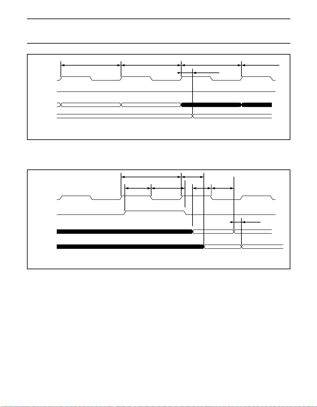
Fig.23 Control register update timing.
The control register data in the SIBDOUT stream is sampled just before the SIB frame is started. This implies that the
returned controlregister data represents the'old' control data, in case new data was providedin the SIBDIN datastream.
sibclk
sibsync
sibdin
sibdout
tsibclk
tsclsy thclsy
tpcldo
tscldi thcldi
Fig.24 Timing definitions SIB interface
tpdido
2000 Jun 26 30
Page 31
Philips Semiconductors Product specification
Advanced modem/audio analog front-end UCB1300
GENERAL PURPOSE I/O
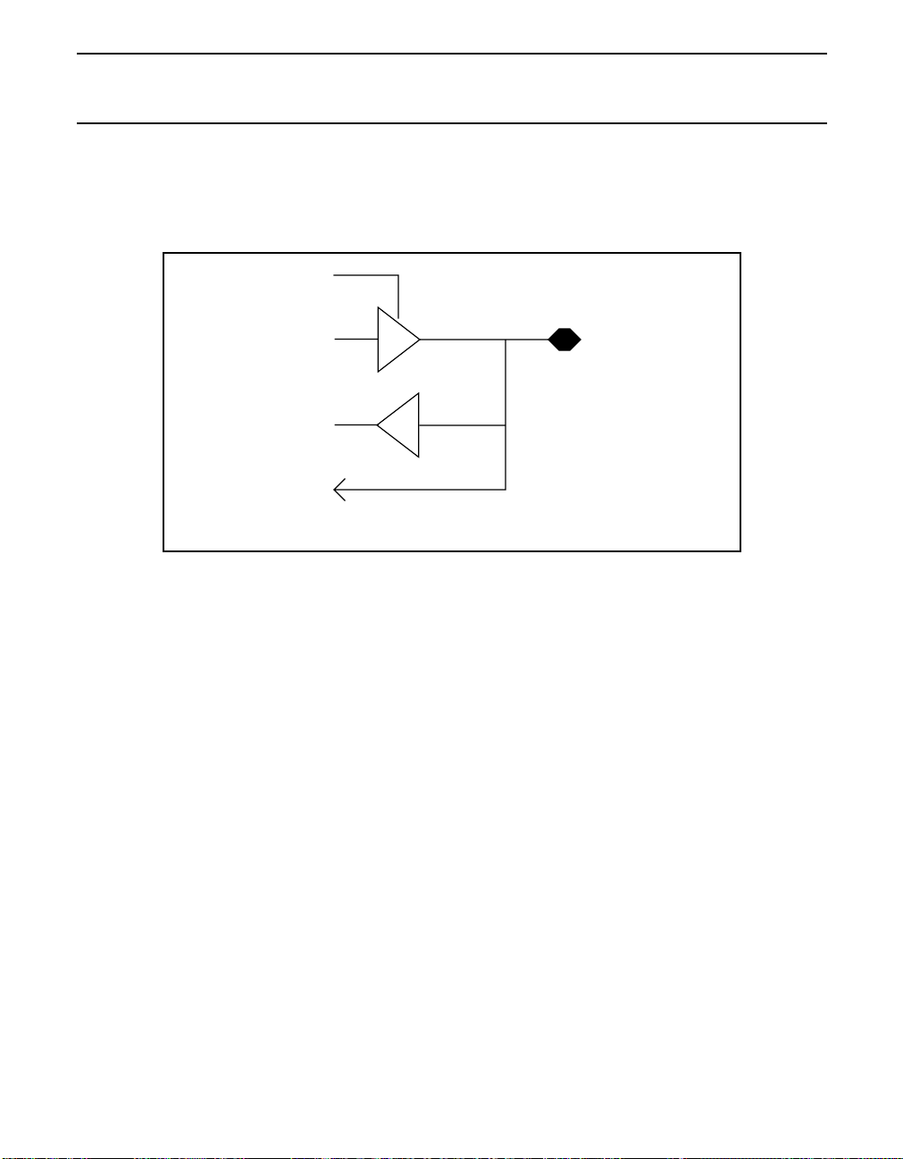
The UCB1300 has 10 programmable digital input/output (I/O) pins. These pins can be independently programmed as
input or output using IO_DIR[0:9] in control register 1. The output data is determined by the content of IO_DATA[n] in
control register 0, while the actual status of these pins can be read from the IO_DATA[n] bits in control register 0.
IO_DIR[n]
IO_DATA[n]
(Write)
IO_DATA[n]
(Read)
to interrupt module
Fig.25 Block diagram of I/O pin circuit.
The data on the IO0-IO9 pins are fed into the interrupt control block, where they can generate an interrupt on the rising
and/or falling edge of these signals.
IO[n]
2000 Jun 26 31
Page 32
Philips Semiconductors Product specification
Advanced modem/audio analog front-end UCB1300
INTERRUPT CIRCUIT
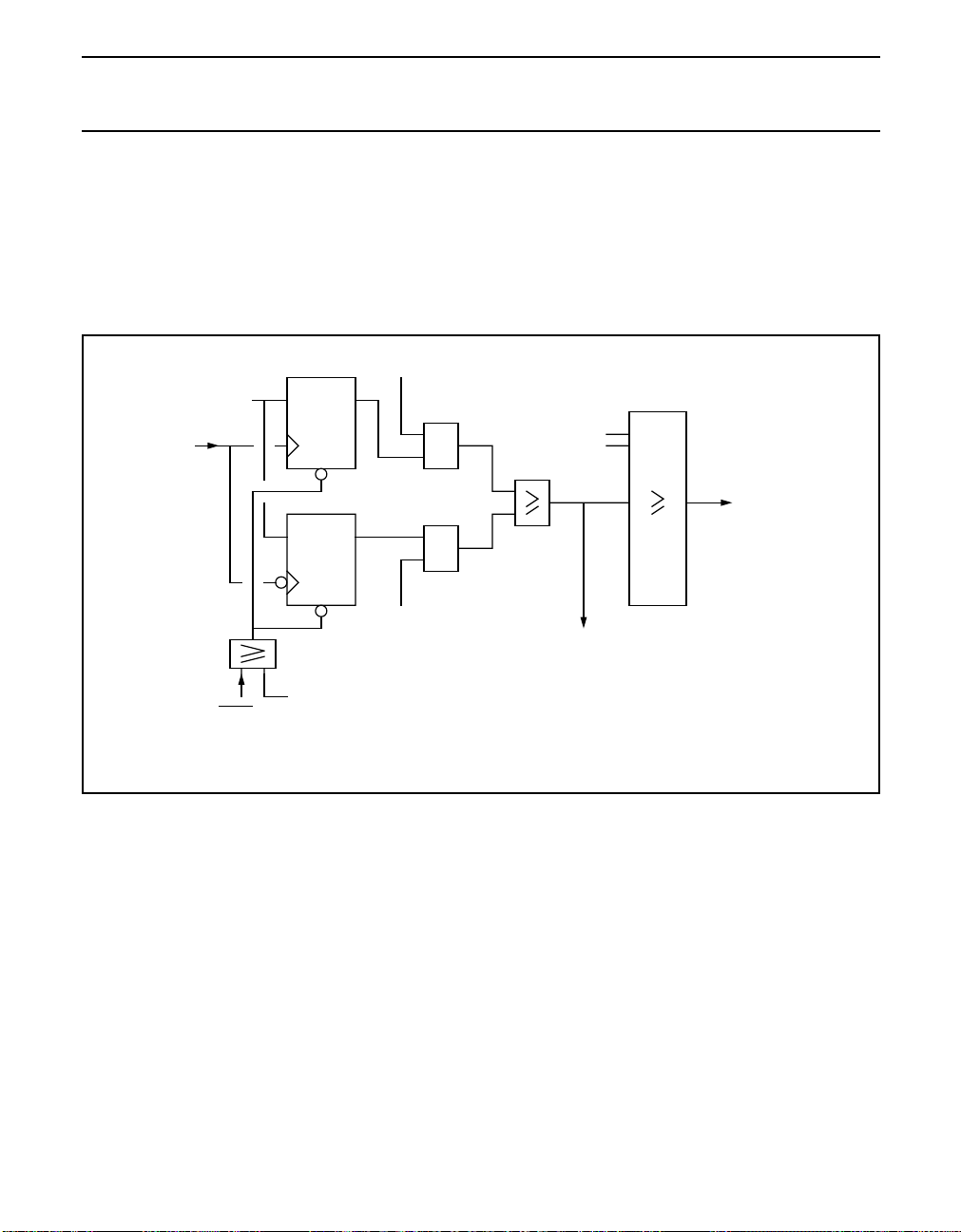
The UCB1300 contains a programmable interrupt control block, which can generate an interrupt for a 0-to-1 and/or a
1-to-0 transition on one or more of the IO0-IO9 pins, the audio and telecom clip detect, the adc_ready signal, and the
TSPX and TSMX signals.
Theinterrupt generationmode isset by IO_RIS_INT[n] in register 2 andINT_FAL_ENA[n] incontrol register3. Theactual
interrupt status of each signal can be read from control register 4. The interrupt status is cleared whenever a 0-to-1
transition is written in control register 4 for the corresponding bit.
rising edge
interrupt enable
interrupt
source
‘1’
DQ
R
DQ
register 2
&
&
‘OR’ tree
IRQOUT
R
falling edge
interrupt enable
register 3
interrupt clear
reset
The IRQOUT pin presents the 'OR' function of all interrupt status bits and can be used to give an interrupt to the system
controller.
The interrupt controller is implemented asynchronously. This provides the possibility to generate interrupts when the
SIBCLK is stopped, e.g. an interrupt can be generated in power down mode, when the touch screen is pressed or when
the state of one of the IO pins changes.
register 4 (write)
Fig.26 Block diagram of the interrupt controller.
interrupt status
register 4 (read)
2000 Jun 26 32
Page 33
Philips Semiconductors Product specification
Advanced modem/audio analog front-end UCB1300
RESET CIRCUIT
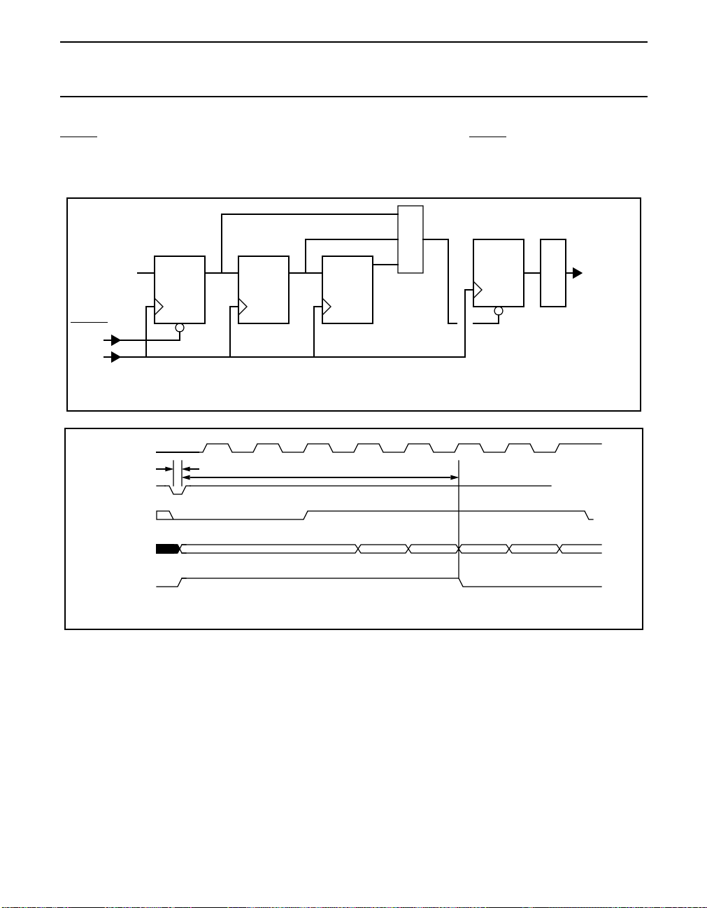
RESET is captured in the UCB1300 using a asynchronous pulse stretching circuit. RESET may be pulled down when
the SIBCLK is still stopped. The internal circuit remembers this reset signal and generates an internal reset signal for at
least 5 SIBCLK periods.
&
RESET
SIBCLK
COUNT
DQ DQ DQ‘1’
R
R
Fig.27 Block diagram of the reset circuit.
<3
internal
reset
sibclk
nreset
arstn
count
internal reset
tlnrst
0123
trsti
Fig.28 Timing diagram of the reset circuit.
2000 Jun 26 33
Page 34
Philips Semiconductors Product specification
Advanced modem/audio analog front-end UCB1300
POWER ROUTING STRATEGY
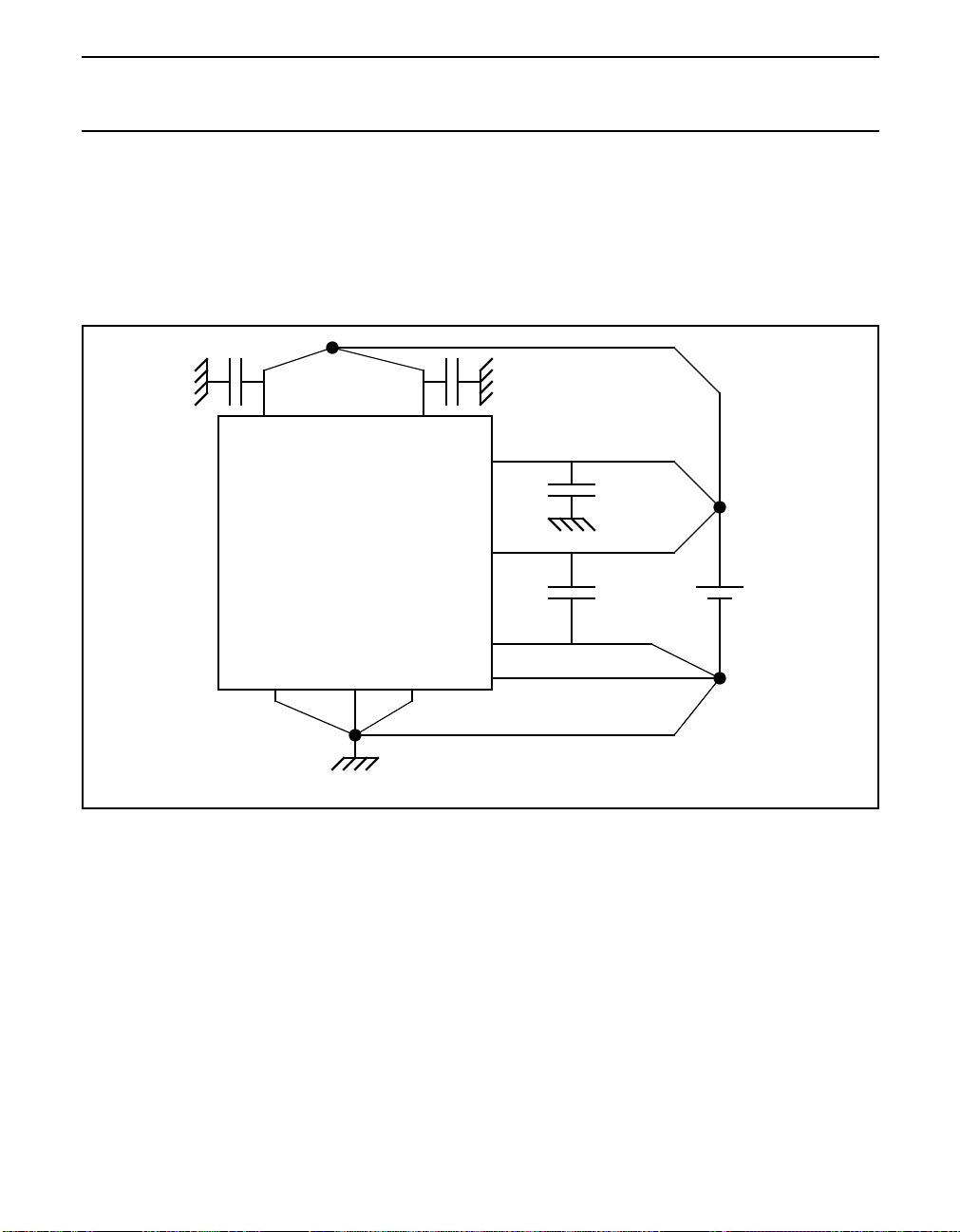
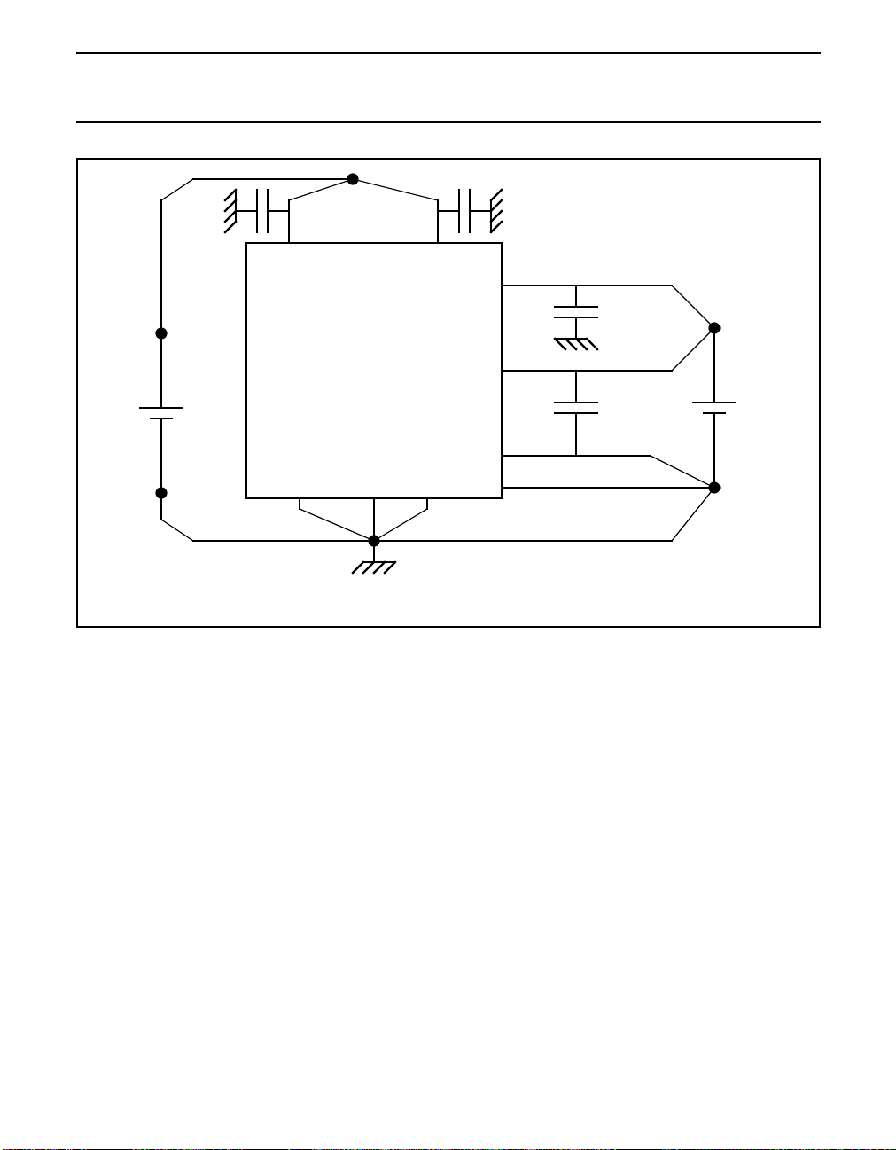
The UCB1300has nine power supply pins,since the UCB1300 contains five power supply regions within the circuit. The
analog anddigital parts havetheir separate power suppliesto reduce theinterference between these parts.The speaker
driver circuit is powered separately (V
has its own ground pin (V
and the touch screen switch matrix, which has relatively large and fluctuating current consumption and the remaining
parts of the analog circuit.
SSA3
DDA2/VSSA2
). This separation in the analog part reduces the interference between the speaker driver
) from the other analog circuit parts, and the touch screen switch matrix
32
vddd vddd
UCB1300
vssd vssd
Fig.29 Recommended power supply connection strategy, single power supply systems.
48
vssa1
18537
vdda1
vdda2
vssa2
vssa3
17
10
26
3.3V supply
7
2000 Jun 26 34
Page 35
Philips Semiconductors Product specification
Advanced modem/audio analog front-end UCB1300
32
48
vddd vddd
vdda1
17
UCB1300
vdda2
10
3.3V
analog
3.3V
digital
supply
vssd vssd
vssa1
18537
vssa2
vssa3
7
26
supply
Fig.30 Recommended power supply connection strategy, dual power supply systems.
The V
and the V
pins and the V
SSD
directly to a ground plane on the PCB. The split in power supply connectionsshould be maintained on the
SSA1
pin are connected within the UCB1300 circuit. It is recommended toconnect the V
SSA1
SSD
pins
PCB to get optimal separation. Fig.29 shows the recommended PCB power supply strategy if only one single supply is
used, while Fig.30 shows the recommended power supply connection for a dual power supply system with separate
analog and digital supplies.
2000 Jun 26 35
Page 36
Philips Semiconductors Product specification
Advanced modem/audio analog front-end UCB1300
APPLICATION INFORMATION
In this chapter some application information is provided. Additional information is also available in the following
application notes (available at www.philips.semiconductors.com)
• AN807: UCB1300 audio codec
• AN809: Differences between UCB1300 and UCB1200
• AN810: DAA printed circuit board layout
• AN812: Data access arrangement (DAA)
Sidetone suppression circuit
UCB1300
TOUTP
11
1:1 transformer
A
Rt
Rt
Ro
TINP
15
Ri
Rs
Rg
+
Rt
B
Rt
14
TINN
Ro
12
TOUTN
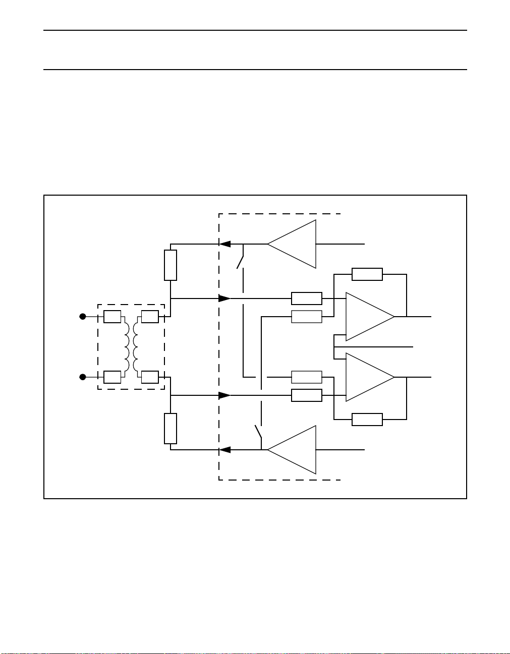
Fig.31 Typical telecom codec sidetone suppression circuit (without protection circuits).
An important built-in feature of the telecom codecis the sidetone suppression circuit. The sidetone suppression circuit is
activated when TEL_SIDE_ENA in the telecom control register B is set. The telecom input signal contains a large part
of the telecom output signal, when the sidetone suppression circuit is disabled. The available dynamic range of the
telecom input is occupied largely by the telecom output voltage.
The sidetone suppression circuit subtracts a part of the telecom output signal from the telecom input signal when
activated. In that case, the available dynamic range is used more effectively than without sidetone suppression.
The built-in side tone suppression circuit, shown in Fig.31, has a fixed subtraction ratio, set be the resistors Rs and Ri,
which equals 600/456. This ratio is calculated from the following relations:
2000 Jun 26 36
Rs
Ri
-
Rg
+
Page 37

Philips Semiconductors Product specification
Advanced modem/audio analog front-end UCB1300
The impedance seen by the telephone line equals:
Z
line
2RtR
×=
RoRi×
++
------------------ -
t
R0Ri+
,
in which Rt represents winding resistance of the transformer, divided by 2. Assuming Ri >> Ro, then:
600
R
lineRtRtRo
--------- 2
300Ω==++=
A typical transformer has 156 Ω winding impedance, thus Roshould be 144 Ω. The ratio of the telecom input and output
voltage is therefore:
V
i(tel)Vo(tel)
156 300+
-----------------------------------------156 300 144++
V
o(tel)
456
×=×=
--------- 600
2000 Jun 26 37
Page 38
Philips Semiconductors Product specification
Advanced modem/audio analog front-end UCB1300
Codec data transfer
The UCB1300 codec operates at samples which depend on the applied SIBCLK frequency and the programmed audio
and telecom divisors. The codec data transfer between the UCB1300 and the system controller has to be synchronized
with theUCB1300 sample counters and theSIB bus data transfer protocol to prevent conversion errors, resulting in high
distortion.
Correct codec data transfer is obtained easily when the UCB1300 is connected to one of the controllers in the PR3000
series, but the UCB1300 can also be connected to other controllers, if the following data protocol is used.
START OF CODEC DATA TRANSFER
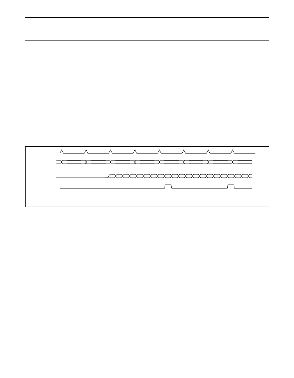
TheUCB1300 internalsample counters are started atthe beginningof thefirst SIBframe followingthe SIB frame in which
the codecinput and/or output pathis enabled. This impliesthat the sample rate divisor has to be programmed before the
codec input and/or output path is enabled, Fig.32.Changing the sample rate on the fly, that is, without disabling both the
codec input and output path before the divisor is reprogrammed, will disturb the codec data transfer synchronization
between the UCB1300 and its controller, and is therefore not allowed.
ADCSYNC
SIBDIN
sample counter
sample frequency
reg. 5 or 7 reg. 6 or 8
012345678012345678012
Fig.32 Start-up sequence of the codec, TEL_DIV[n] = 9.
2000 Jun 26 38
Page 39
Philips Semiconductors Product specification
Advanced modem/audio analog front-end UCB1300
CODEC DATA TRANSFER INTO THE UCB1300
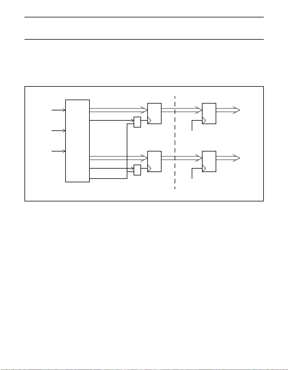
Boththe audio andthe telecom data is transferredwithin the SIB frame (bit11-0 and bit47-32). Thisdata is accompanied
by two data valid flags (bit 30: audio data valid; bit 31: telecom data valid). The codec data in the SIB frames is only
processed in the UCB1300 if the appropriate data valid flag is set in the frame; the data is discarded when the data flag
equals ‘0’. Figure 33 shows the basic codec data synchronization principle used in the UCB1300.
SIB INTERFACE
SIBCLK
SIBDIN
SIBSYNC
Figure 33 shows that audio and telecom data is made available for the codec up sample filters during the 64th bit in the
SIB frame. This implies that the codec data has to be transferred in one of the SIB frames preceding the codec sample
moment.
Note: If the programmed divisor equalsa multipleof 4,the codec datatransfer issynchronized tothe SIB frame repetition
rate (e.g. AUD_DIV[n] = 8 ⇒1 sample is needed in 2 SIB frames, AUD_DIV[n] = 12 ⇒ 1 sample is needed in 3 SIB
frames, etc.).
audio data[n]
audio_data_valid
telecom data[n]
64-bit shift register
telec_data_valid
bit64
Fig.33 Codec input path data synchronization principle.
DFF
&
DFF
&
UP-SAMPLE FILTERS
input
latch
fsa
input
latch
fst
2000 Jun 26 39
Page 40
Philips Semiconductors Product specification
Advanced modem/audio analog front-end UCB1300
CODEC DATA TRANSFER FROM THE UCB1300
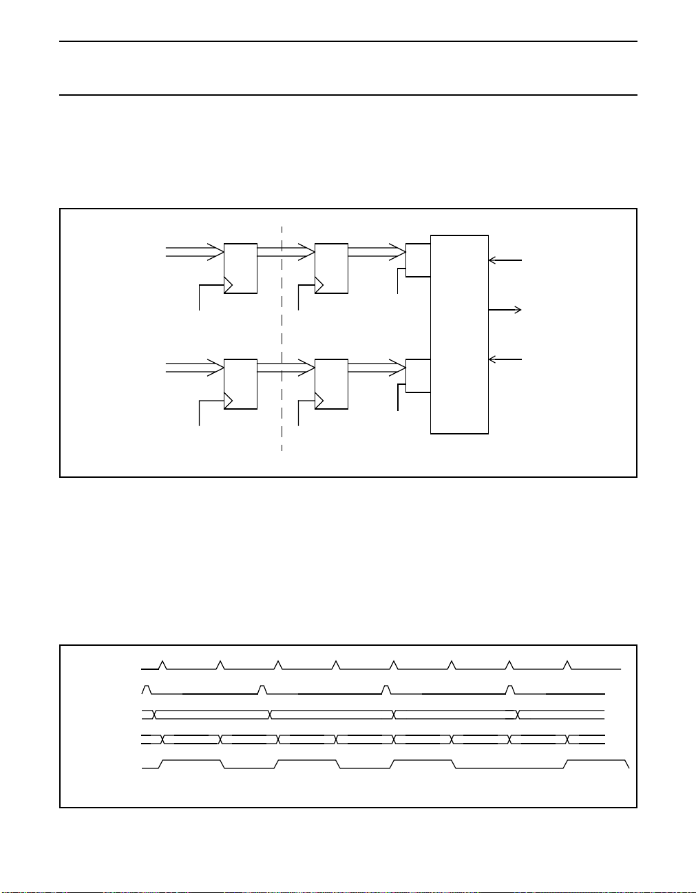
The data resulting from the UCB1300 codec ADC (input) paths is transfer to the system controller at the programmed
codecsample rate. However the codecdata issynchronized withthe SIB frame repetition rate.Figure 34shows thebasic
synchronization principle used inside the UCB1300. Codec data will be present in each SIB frame produced by the
UCB1300; the sample will be repeated in the following SIB frames till a new sample has become available.
DOWN SAMPLE FILTERS
output
audio data[n]
DFF
SIB INTERFACE
load
SIBCLK
latch
fsa
bit0
bit21
SIBDOUT
telec data[n]
SIBSYNC
output
DFF
load
64-bit shift register
latch
bit48
fst bit21
Fig.34 synchronization of codec samples in SIBDOUT data stream.
The codec samples in the SIBDOUT stream are also accompanied by a audio and telecom data valid bit (bit 30 and
bit 31). These datavalid flags are zero if the corresponding codec ADCpaths are disabled and during the start up period
of the codec’s, when unreliable samples are generated. By default (after reset), the data valid bits will be continuously
‘1’ when reliable samples are generated.
However when DYN_VFLAG_ENA is set, the data valid bits will be ‘1’ during one of the SIB frames, containing identical
samples (this is the case when a high divisor is programmed). The audio_vflag bit will be high during the last sample in
a series of identicalsamples, while the telecom_vflag bitis high atthe firstsample in aseries of identical bits. Anexample
of the timing diagram is shown in Figure 35.
SIBSYNC
fsa
audio codec out
SIBDOUT
audio_vflag bit
sample N
sample N sample N sample N+1
sample N+1
Fig.35 Audio codec data transfer, AUD_DIV[n] = 9, DYN_VFLAG_ENA = 1.
2000 Jun 26 40
sample N+1
sample N+2
sample N+2 sample N+2 sample N+2
sample N+3
sample N+3
Page 41
Philips Semiconductors Product specification
Advanced modem/audio analog front-end UCB1300
LIMITING VALUES
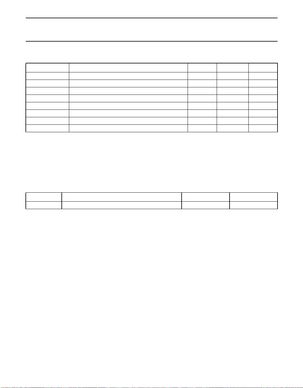
In accordance with the Absolute Maximum Rating System (IEC 134); notes 1 and 2
SYMBOL PARAMETER MIN. MAX. UNIT
V
DD
V
I
V
I
V
O
I
I(d)
I
O(d)
I
O
T
stg
Notes
1. Stresses above those listed under Absolute Maximum Ratings may cause permanent damage to the device. This is
a stress rating only and functional operation of the device at these or any conditions other than those described in
the Absolute Maximum Rating section of this specification is not implied.
2. Parameters arevalid over the ambient operating temperature range unless otherwise specified. Allvoltages are with
respect to V
supply voltage -0.5 +5.0 V
DC input voltage (except inputs AD0 - AD3) -0.5 VDD+ 0.5 V
DC input voltage AD0 - AD3 -0.5 +8.5 V
DC output voltage - VDD+ 0.5 V
diode input current - 10 mA
diode output current - 10 mA
continuous output current, digital outputs - 4 mA
storage temperature range -55 +150 °C
(pin 37), unless otherwise noted.
SSD
THERMAL CHARACTERISTICS
SYMBOL PARAMETER VALUE UNIT
R
th(j-a)
thermal resistance from junction to ambient in free air 67 K/W
2000 Jun 26 41
Page 42
Philips Semiconductors Product specification
Advanced modem/audio analog front-end UCB1300
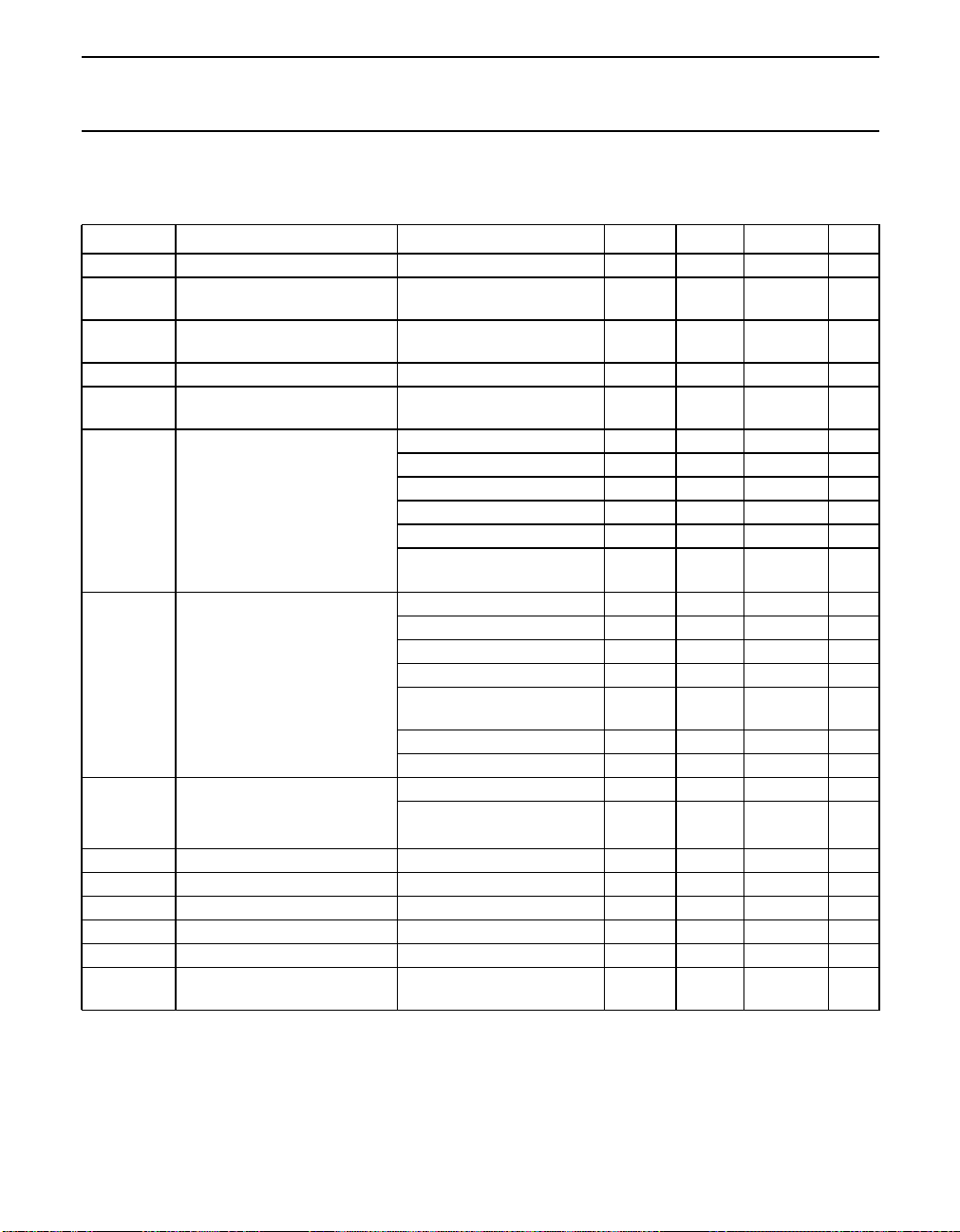
DC CHARACTERISTICS
V
SSD=VSSA1=VSSA2=VSSA3
(pin 5); unless otherwise specified.
SYMBOL PARAMETER CONDITIONS MIN. TYP. MAX. UNIT
V
V
DDD
DDA1
digital supply voltage 3.0 3.3 3.6 V
analog supply voltage - excl.
speaker driver
V
DDA2
analog supply voltage -
speaker driver only
V
V
SSA2
SSA3
analog ground - speaker driver -0.4 0 +0.4 V
analog ground - touch screen
switch matrix
I
DDD
I
DDA1
I
DDA2
digital supply current
analog supply current
total speaker driver supply
current
=0V; T
(1)
(1)(2)
amb
(1)(2)
=25 °C; f
= 9.216 MHz; V
i(sibclk)
= 1.2 V; all voltages referenced to V
I(ref)
3.0 3.3 3.6 V
3.0 3.3 3.6 V
-0.4 0 +0.4 V
full functionality 19 - mA
only audio codec activated - 17 - mA
only telecom codec activated - 19 - mA
only touch screen activated - 15 - mA
only ADC activated - 15 - mA
no functions activated; f
--10µA
sibclk
off
full functionality - 4.6 - mA
only audio codec activated - 3.7 - mA
only telecom codec activated - 4.4 - mA
only touch screen activated - 1.0 - mA
only touchscreen in interrupt
- - 100 µA
mode
only ADC activated - 1.0 - mA
no analog functions activated - <10 - µA
speaker driver enabled - 0.6 - mA
speaker driver disabled - - 10 µA
SSD
V
IL
V
IH
V
OL
V
OH
f
i(sibclk)
T
amb
LOW level input voltage -0.5 - +0.3V
HIGH level input voltage 0.7V
LOW level output voltage IOL= 2 mA - - 0.2V
HIGH level output voltage IOH= 2 mA 0.8V
serial interface clock frequency 0 10 15 MHz
operating ambient temperature
range
Notes
1. Indicative value measured during the initial characterization.
2. Excluding connected touch screen and speaker load currents.
2000 Jun 26 42
V
DDD
- 0.5V
DDD
-- V
DDD
DDD
DDD
V
V
-20 - 70 °C
Page 43
Philips Semiconductors Product specification
Advanced modem/audio analog front-end UCB1300
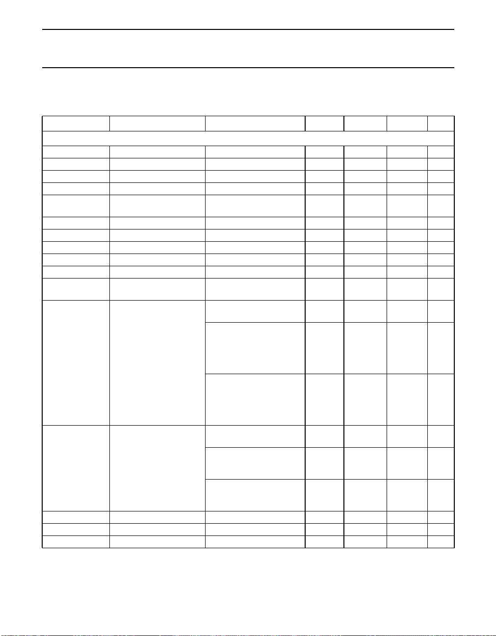
AC CHARACTERISTICS
V
SSD=VSSA1=VSSA2=VSSA3
f
= 9.216 MHz; unless otherwise specified.
i(sibclk)
SYMBOL PARAMETER CONDITIONS MIN. TYP. MAX. UNIT
Audio Input; notes 1 and 2
f
sa
V
I(RMS)
V
I(BIAS)
Z
i
Z
(18-20)
audio sample frequency - - 26 kHz
input voltage (RMS value) 0 dB gain setting 90 100 125 mV
DC bias voltage MICP input 1.35 1.4 1.5 V
input impedance 20 25 - kΩ
impedance MICGND -
VSSA1
G
step
N
step
G
v
E
G
gain step size 1 1.5 2 dB
number of gain settings - 32 - gain (AUD_GAIN=011111) 15 22.5 28 dB
gain error each gain step -1 - 1 dB
RES resolution - 12 - bit
LE
(d)(ADC)
ADC differential linearity
error
THD total harmonic distortion input gain = 0 dB
S/N signal-to-noise ratio input gain = 0 dB
PBRR pass-band ripple rejection f
SBR stop-band rejection f
D
offset
digital offset no signal applied to MICP - - 50 LSB
=0V; V
DDD=VDDA1=VDDA2
= 3.3 V ±10%; T
(AUD_GAIN = 00000);
input signal = 1 mVrms
input gain = 22.5 dB
(AUD_GAIN[n] = 01111);
AC coupling disabled
(AUD_OFF_CAN = 0);
input signal = 0.4mVrms
input gain = 46.5 dB
(AUD_GAIN[n] = 11111);
AC coupling enabled
(AUD_OFF_CAN = 1);
(AUD_GAIN = 00000)
input signal = 1mVrms;
input gain = 22.5 dB
(AUD_GAIN[n] = 01111);
input signal = 0.4mVrms;
input gain = 46.5 dB
(AUD_GAIN[n] = 11111);
pla<fsig<fpha
sha<fsig
(3)
< 20 kHz
(3)
amb
=25 °C; V
I(ref)
= 1.2 V;
- - 200 Ω
- - 1 LSB
- -65 -40 dB
- -36 -26 dB
-29 dB
50 68 - dB
25 32 - dB
22 dB
- - 1.2 dB
50 - - dB
2000 Jun 26 43
Page 44
Philips Semiconductors Product specification
Advanced modem/audio analog front-end UCB1300
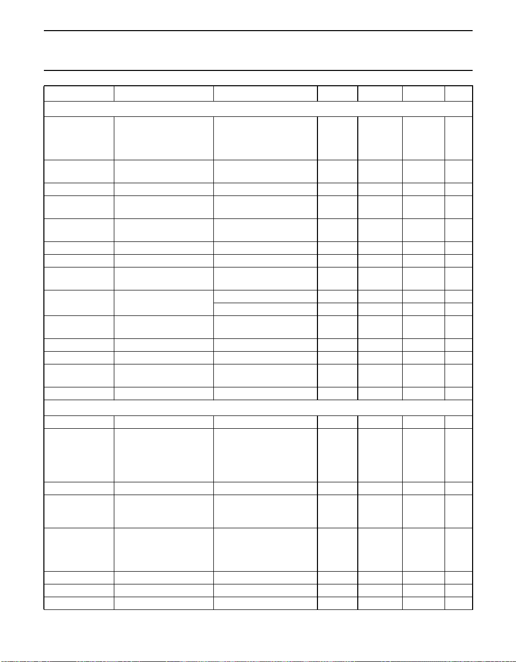
SYMBOL PARAMETER CONDITIONS MIN. TYP. MAX. UNIT
Audio Output; notes 4 and 5
V
O(RMS)
E
offset
V
O(BIAS)
α
step
N
step
α attenuation 63 69 75 dB
RES resolution - 12 - bit
LE
(d)(DAC)
THD total harmonic distortion - - -35 dB
S/N signal-to-noise ratio 16 Ω speaker; 100 Hz to
PBRR pass-band ripple rejection f
SBR stop-band rejection f
OBR
(RMS)
Z
speaker
Telecom Input; notes 2 and 7
f
st
V
I(RMS)
V
I(BIAS)
i
α
i
Z
i
S/N signal-to-noise ratio 65 75 - dB
THD total harmonic distortion - -76 -65 dB
output voltage (RMS
value)
attenuation = 0 dB,
differentially measured
1.0 1.25 1.5 V
between SKPRN and
SPRKP
offset error (peak-to-peak
- - 100 mV
value)
DC bias voltage SPKRP/SKPRN 1.2 1.4 1.6 V
attenuation step size
2.5 3.0 3.5 dB
(analog section)
number of attenuation
-24- -
steps
DAC differential linearity
- - 1 LSB
error
1kΩ headphone load - - -45 dB
40 - - dB
20 kHz bandwidth
out-of-band rejection
pla<fsig<fpha
sha<fsig
(6)
< 20 kHz
(6)
f > 20 kHz - - 50 mV
- - 1.2 dB
50 - - dB
(RMS value)
speaker impedance 8 16 - Ω
sample frequency - - 10 kHz
input voltage (RMS value) differentially applied to
330 370 410 mV
TINN and TINP;
no I/P attenuation enabled
(TEL_ATT = 0,
TEL_GAIN = 0)
DC bias voltage TINN/TINP 1.2 - 1.6 V
input attenuation input attenuation
-6.5 -6 -5.5 dB
amplification enabled
(TEL_ATT = 1)
input attenuation gain input attenuation
5.5 6 6.5 dB
amplification enabled
(TEL_ATTAMPL = 1,
TEL_ATT = 0)
input impedance 25 - - kΩ
2000 Jun 26 44
Page 45
Philips Semiconductors Product specification
Advanced modem/audio analog front-end UCB1300
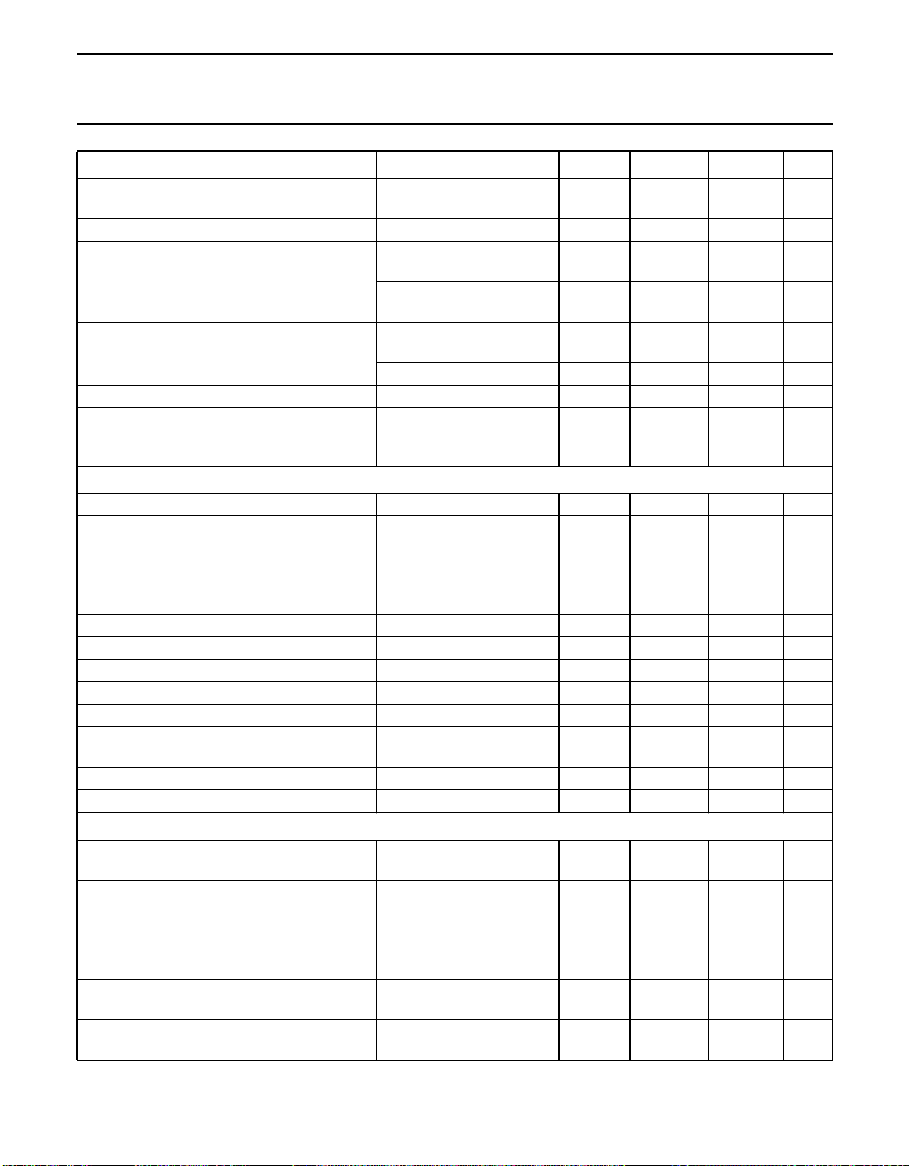
SYMBOL PARAMETER CONDITIONS MIN. TYP. MAX. UNIT
LE
(d)(ADC)
RES resolution - 14 - bit
PBRR pass-band ripple rejection f
SBR stop-band rejection f
D
offset
S
sup
Telecom output; note 5
f
st
V
O(RMS)
V
O(BIAS)
RES resolution - 14 - bit
S/N signal-to-noise ratio 65 75 - dB
THD total harmonic distortion - -76 -65 dB
PBRR pass-band ripple rejection - - 1.2 dB
SBR stop-band rejection f
OBR
(RMS)
Z
o(load)
E
offset
Touch screen
V
I(BIAS)
I touch screen current touch screen position
R
i
R
gs
R
ps
ADC differential linearity
- - 2 LSB
error
plt<fsig<fpht
(8)(16)
filter
f
vht<fsig<fpht
sig<fvlt
sht<fsig
(8)(16)
; voice filter
(8)(16)
(8)(16)
activated
activated
f
; no voice
; voice filter
- - 1.2 dB
- - 1.2 dB
30 - - dB
50 - - dB
digital offset no signal applied to MICP - - 50 LSB
sidetone suppression
effectiveness
600 Ω line impedance; 1:1
transformer with 156 Ω
20 - - dB
winding resistance
sample frequency - 8 - kHz
output voltage (RMS
value)
differentially measured
between TOUTP and
1.35 - 1.85 V
TOUTN
DC bias voltage TOUTP/TOUTN; telecom
1.2 - 1.6 V
O/P path enabled
(9)
out-of-band rejection
sht
f> f
< f < f
(9)(16)
st
st
70 - - dB
- - 25 mV
(RMS value)
load impedance 600 Ω
offset error note 10 - - 100 mV
bias voltage touch screen position
1.6 1.8 2.0 V
mode selected
10 - - mA
mode selected
Max. touch screen
resistance to generate an
touch screen interrupt
mode selected
- - 2500 Ω
interrupt
ground switch on
-- 50Ω
resistance
power switch on
-- 50Ω
resistance
2000 Jun 26 45
Page 46
Philips Semiconductors Product specification
Advanced modem/audio analog front-end UCB1300
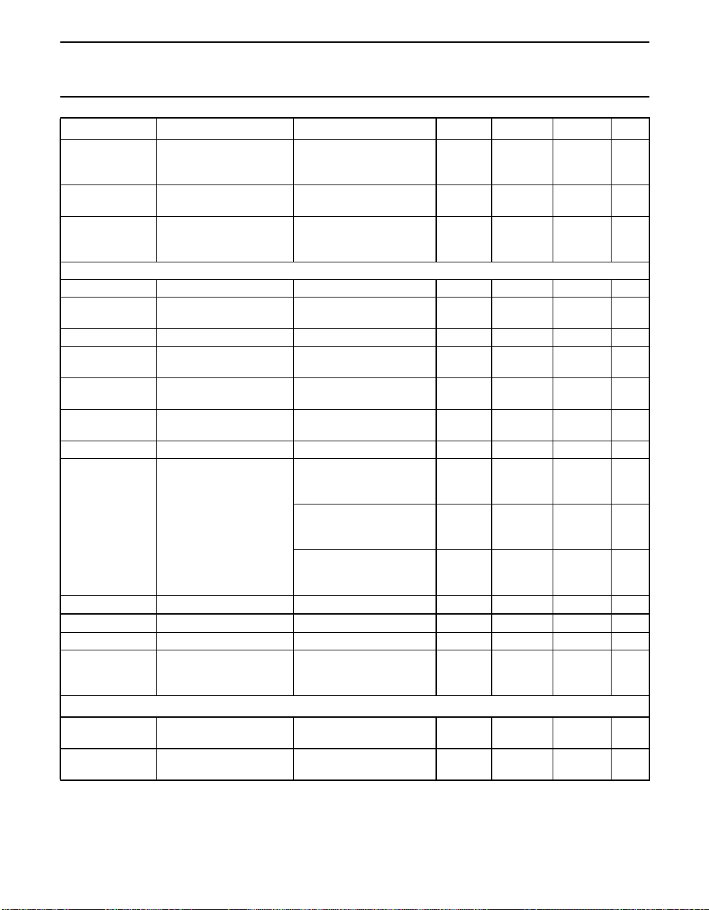
SYMBOL PARAMETER CONDITIONS MIN. TYP. MAX. UNIT
t
STRTU
Eidle Idle pressure reading pressure mode selected,
∆light_touch Pressure reading:
ADC; notes 11 and 12
RES resolution - 10 - bit
V
I(AD0-AD3)
Z
i
I
LI
LE
(d)(ADC)
LE
(i)(ADC)
t
en(ADC)
t
d(s)
t
conv
t
track
t
adcsync
t
sibwrite
On-chip reference circuit
V
i(ref)
t
STRTU
start up time of touch
-- 25µs
screen bias voltage
generator
30 120 LSB
open (no current drawn)
light-touch - 1.25xEidle
pressure mode selected,
(18)
2.2kΩ for light touch, open
40 250 LSB
for idle
full scale AD0 - AD3
7.0 7.5 8.0 V
inputs
input impedance 50 75 100 kΩ
input leakage current V
ADC differential linearity
ADO=VAD1=VAD2
V
= 7.5 V
AD3
=
- - 2 LSB
10 µA
error
ADC integral linearity
5 - 95% of full scale - - 3 LSB
error
ADC enable time 5 - - µs
sampling delay nonsynchronizationmode;
-4t
SIBCLK
-ns
no changing ADC
multiplexer settings
nonsynchronization mode;
- 51t
SIBCLK
-ns
changing ADC multiplexer
settings
synchronization mode;
t
SIBCLK
1.5t
SIBCLK
ns
rising edge ADCSYNC to
sample moment
conversion time - 102t
tracking time 5t
SIBCLK
49t
SIBCLK
SIBCLK
-ns
ns
ADCSYNC pulse width 5 - - ns
control register update
- 65t
SIBCLK
-ns
after SIBSYNC falling
edge
reference voltage applied
1.0 1.2 1.4 V
to VREFBYP
start-up time of internal
- - 50t
SIBCLK
ns
reference voltage circuit
2000 Jun 26 46
Page 47
Philips Semiconductors Product specification
Advanced modem/audio analog front-end UCB1300
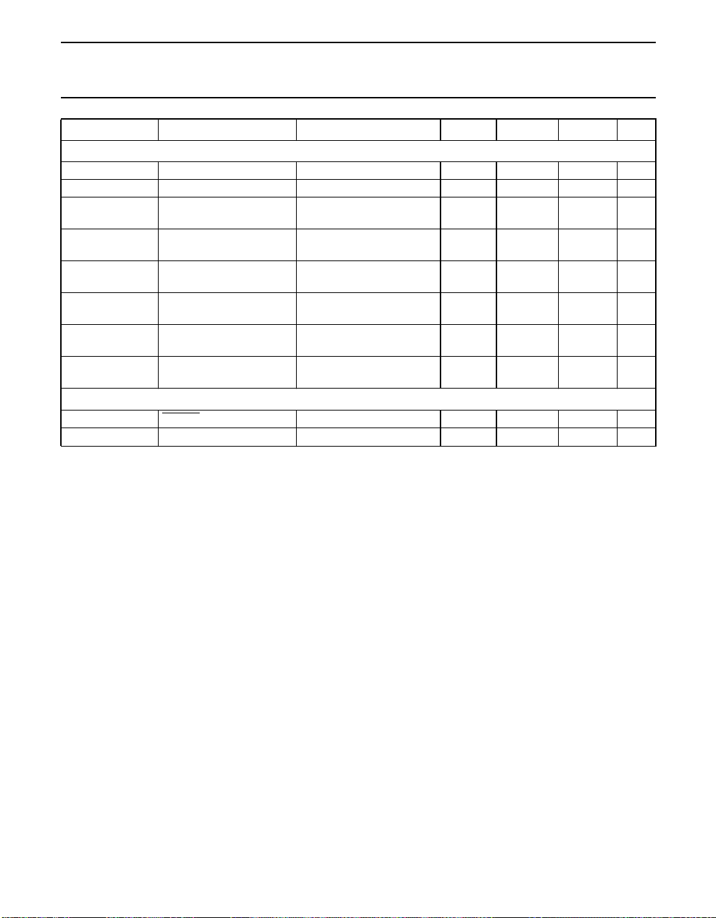
SYMBOL PARAMETER CONDITIONS MIN. TYP. MAX. UNIT
Control register data transfer
f
i(sibclk)
δ
(sibclk)
t
su(SIBSYNC-SIBCLK)
t
h(SIBSYNC-SIBCLK)
t
su(SIBDIN-SIBCLK)
t
h(SIBDIN-SIBCLK)
t
(SIBCLK-SIBDOUT)
t
(SIBDIN-SIBDOUT)
Reset circuit
t
W(NRESET)
t
W(rst)
Notes
1. Additional test conditions: AUD_DIV[n] = 00001100; input signal 1 kHz, 90 mV (RMS); AUD_IN_ENA =1.
2. Coding system for ADC output data is 2’s complement.
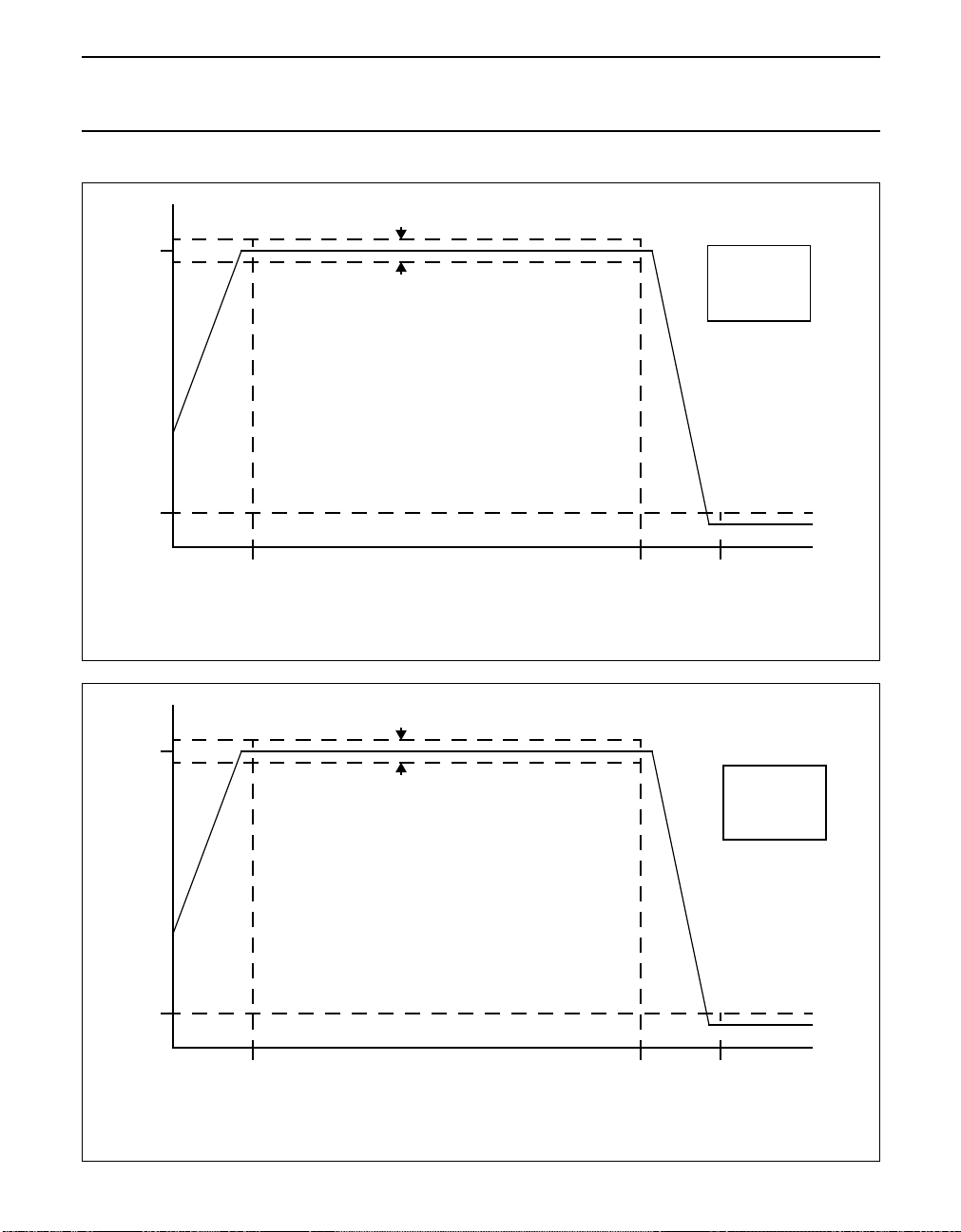
3. See Fig. 36.
4. Additional test conditions: AUD_DIV[n] = 00001100; 0 dB output attenuation; 90% of digital full scale input voltage;
16 Ω speaker connected.
5. Additional test conditions: TEL_DIV[n] = 0101000; 0 dB output attenuation; 90% of digital full scale input voltage;
1200 Ω load.
Coding system for DAC input data is 2’s complement.
6. See Fig. 37.
7. Additional test conditions: TEL_DIV[n] = 0101000; input signal 1 kHz, 300 mV (RMS); TEL_IN_ENA = 1;
TEL_VOICE_ENA = 0.
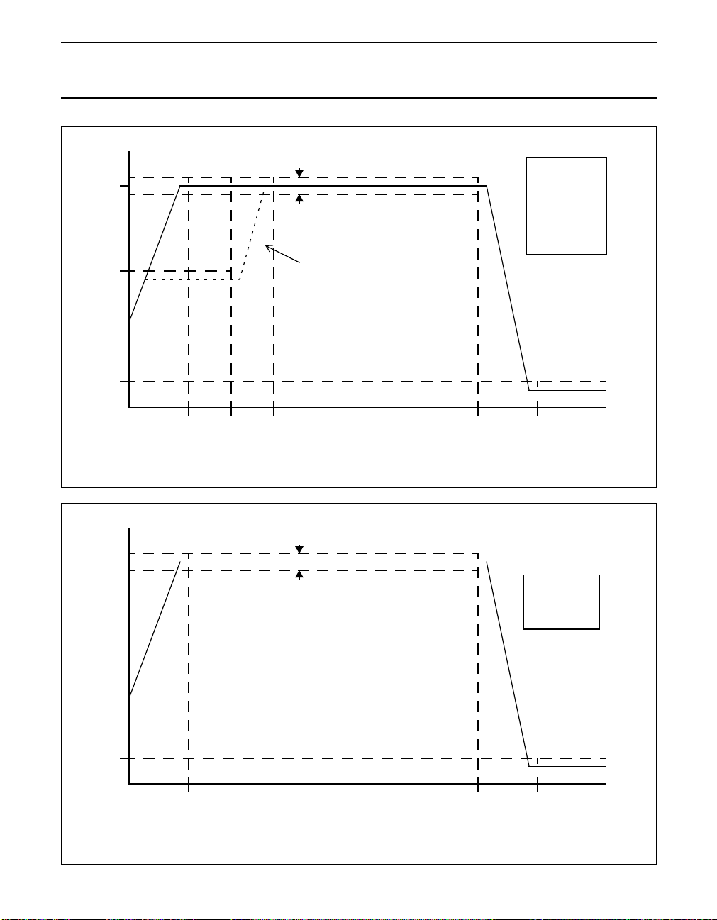
8. See Fig. 38.
9. See Fig. 39.
10. Deviation of the analog output from 0, with 0 code input to telecom output path.
11. The ADC cannot be started or armed if the touch screen circuit is set to interrupt mode (TSC_MODE[n] = 0,0).
12. Coding system for ADC is binary offset.
13. This is a requirement when an odd divisor is set in either the audio or the telecom codec.
14. This is valid for all SIB frame bits 0 to 63, except bits 17 to 20.
15. This is valid for a the SIB frame bits 17 to 20.
16. All curves repeat around the sample frequency fsa or fstfor audio- respectively telecom codec.
17. Any touch-screen resistor above the maximum will not reach full scale and not saturate the ADC.
18. The threshold can be used to verify a valid touch using pressure measurement.
SIBCLK input frequency 0 - 15 MHz
SIBCLK duty factor note 13 - 50 - %
set-up time SIBSYNC to
-15- ns
SIBCLK falling edge
SIBSYNC hold time after
-10- ns
falling edge of SIBCLK
set-up time SIBDIN to
-15- ns
SIBCLK falling edge
SIBDIN hold time after
-10- ns
falling edge of SIBCLK
rising edge of SIBCLK to
note 14 - 10 - ns
valid SIBDOUT
valid SIBDIN to valid
note 15 - 15 - ns
SIBDOUT
RESET pulse width 5 - - ns
internal reset pulse width 5t
SIBCLK
-ns
2000 Jun 26 47
Page 48
Philips Semiconductors Product specification
Advanced modem/audio analog front-end UCB1300
FREQUENCY RESPONSE CURVES
RIPia
0dB
SBRia
0dB
Fpla Fpha FshaFrequency [Hz]
Fig.36 Audio input path frequency response.
RIPoa
f
0.0016 fsa×=
pla
0.42 fsa×=
f
pha
0.6 fsa×=
f
sha
f
0.0016 fsa×=
pla
f
0.42 fsa×=
pha
0.6 fsa×=
f
sha
SBRoa
Fpla Fpha FshaFrequency [Hz]
Fig.37 Audio output filter frequency response.
2000 Jun 26 48
Page 49
Philips Semiconductors Product specification
Advanced modem/audio analog front-end UCB1300
0dB
SBRvti
SBRsht
0dB
Fplt
RIPti
Voice filter enabled
Fvlt Fvht
Frequency [Hz]
Fig.38 Telecom input frequency response
RIPto
Fpht
f
plt
f
pht
f
sht
f
vlt
f
vht
Fsht
f
plt
f
pht
f
sht
0.0016 fst×=
0.42 fst×=
0.6 fst×=
0.018 fst×=
0.05 fst×=
0.0016 fst×=
0.42 fst×=
0.6 fst×=
SBRhto
Fplt Fpht
Frequency [Hz]
Fig.39 Telecom output frequency response.
2000 Jun 26 49
Fsht
Page 50
Philips Semiconductors Product specification
Advanced modem/audio analog front-end UCB1300
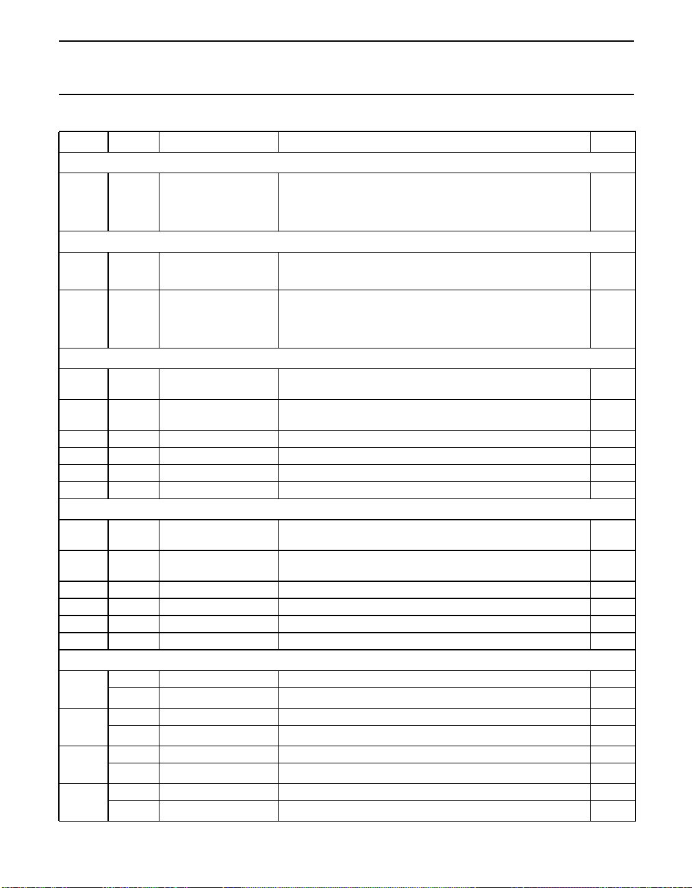
CONTROL REGISTER OVERVIEW
BIT MODE SYMBOL REMARK RESET
Address 0: I/O port data register
0 to 9 R/W IO_DATA[n] The bits in the write register provide the data of the I/O pin
when programmed as output.
The bits in the read register return the actual state of the
associated I/O pin.
Address 1: I/O port direction register
0 to 9 R/W IO_DIR[n] If '1', the associated I/O pin is defined as output.
If ‘0', the associated I/O pin is defined as input.
0
0
15 R/W SIB_ZERO If ‘1’, the SIBDOUT pin is forced ‘0’ during the second SIB
word.
If '0', the SIBDOUT pin is three-stated during the second SIB
word.
Address 2: Rising edge interrupt enable register
0 to 9 R/W IO_RIS_INT[n] If '1', the rising edge interrupt of the associated I/O pin is
enabled.
11 R/W ADC_RIS_INT If '1', the rising edge interrupt of the adc_ready signal is
enabled.
12 R/W TSPX_RIS_INT If '1', the rising edge interrupt of the TSPX signal is enabled. 0
13 R/W TSMX_RIS_INT If '1', the rising edge interrupt of the TSMX signal is enabled. 0
14 R/W TCLIP_RIS_INT If '1', the rising edge interrupt of the telecom clip is enabled. 0
15 R/W ACLIP_RIS_INT If '1', the rising edge interrupt of the audio clip is enabled. 0
Address 3: Falling edge interrupt enable register
0 to 9 R/W IO_FAL_INT[n] If '1', the falling edge interrupt of the associated I/O pin is
enabled.
11 R/W ADC_FAL_INT If '1', the falling edge interrupt of the adc_ready signal is
enabled.
12 R/W TSPX_FAL_INT If '1', the falling edge interrupt of the TSPX signal is enabled. 0
13 R/W TSMX_FAL_INT If '1', the falling edge interrupt of the TSMX signal is enabled. 0
14 R/W TCLIP_FAL_INT If '1', the falling edge interrupt of the telecom clip is enabled. 0
15 R/W ACLIP_FAL_INT If '1', the falling edge interrupt of the audio clip is enabled. 0
Address 4: Interrupt clear/status register
0 to 9 W IO_INT_CLR[n] A0-to-1 transition clears the interrupt of the associated I/O pin. 0
R IO_INT_STAT[n] Returns the actual interrupt status of the associated I/O pin 0
11 W ADC_INT_CLR A 0-to-1 transition clears the interrupt adc_ready signal. 0
R ADC_INT_STAT Returns the actual interrupt status of the adc_ready signal. 0
12 W TSPX_INT_CLR A 0-to-1 transition clears the interrupt of the TSPX signal. 0
R TSPX_INT_STAT Returns the actual interrupt status of the TSPX signal. 0
13 W TSMX_INT_CLR A 0-to-1 transition clears the interrupt of the TSMX signal. 0
R TSMX_INT_STAT Returns the actual interrupt status of the TSMX signal. 0
0
0
0
0
0
2000 Jun 26 50
Page 51
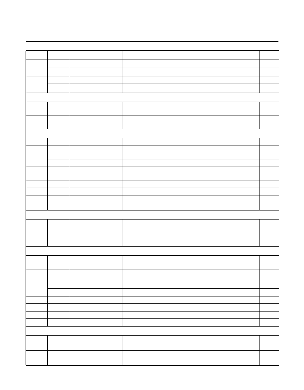
Philips Semiconductors Product specification
Advanced modem/audio analog front-end UCB1300
BIT MODE SYMBOL REMARK RESET
14 W TCLIP_INT_CLR A 0-to-1 transition clears the interrupt of the telecom clip. 0
R TCLIP_INT_STAT Returns the actual interrupt status of the telecom clip. 0
15 W ACLIP_INT_CLR A 0-to-1 transition clears the interrupt of the audio clip. 0
R ACLIP_INT_STAT Returns the actual interrupt status of the audio clip. 0
Address 5: Telecom control register A
0 to 6 R/W TEL_DIV[n] Telecom codec sample rate divisor. Valid values lie
between16 [0010000] and 127 [1111111].
7 R/W TEL_AMPL If '1', the additional input gain of the telecom codec is enabled
(+6dB).
Address 6: Telecom control register B
3 R/W TEL_VOICE_ENA If '1', the voice band filter in the telecom input path is enabled. 0
4 R TEL_CLIP_STAT Returns the telecom clip detection status. (the telecom clip
status will remain set until cleared by the user).
W TEL_CLIP_CLR A 0-to-1 transition clears the telecom clip detection status. 0
6 R/W TEL_ATT If '1', the telecom input attenuation (-6 dB) is enabled. This
control overrides the TEL_AMPL control.
11 R/W TEL_SIDE_ENA If '1', the sidetone suppression circuit is activated. 0
13 R/W TEL_MUTE If '1', the telecom output is muted. 0
14 R/W TEL_IN_ENA If '1', the telecom input path is activated. 0
15 R/W TEL_OUT_ENA If '1', the telecom output path is activated. 0
Address 7: Audio control register A
0 to 6 R/W AUD_DIV[n] Audio codec sample rate divisor. Valid values lie between
6 [0000110] and 127 [1111111].
7 to 11 R/W AUD_GAIN[n] Audio input gain setting. Values range from 0 dB [00000] to
46.5 dB [11111]
Address 8: Audio control register B
0 to 4 R/W AUD_ATT[n] Audio output attenuation setting. Values range from 0 dB
[00000] to 69 dB [11111].
6 R AUD_CLIP_STAT Returns the audio clip detection status. If '1', the audio clip
detection circuit is activated (The audio clip status will remain
set until it is cleared by the user)
W AUD_CLIP_CLR If 0-to-1 transition, clears the audio clip detection status. 0
8 R/W AUD_LOOP If '1', the loopback mode in the audio codec is activated. 0
13 R/W AUD_MUTE If '1', the audio output is muted. 0
14 R/W AUD_IN_ENA If '1’, the audio codec input path is activated. 0
15 R/W AUD_OUT_ENA If '1', the audio codec output path is activated. 0
Address 9:Touch screen control register
0 R/W TSMX_POW If ‘1’, the TSMX pin is powered. 0
1 R/W TSPX_POW If ‘1’, the TSPX pin is powered. 0
2 R/W TSMY_POW If ‘1’, the TSMY pin is powered. 0
3 R/W TSPY_POW If ‘1’, the TSPY pin is powered. 0
16
0
0
0
9
0
0
0
2000 Jun 26 51
Page 52
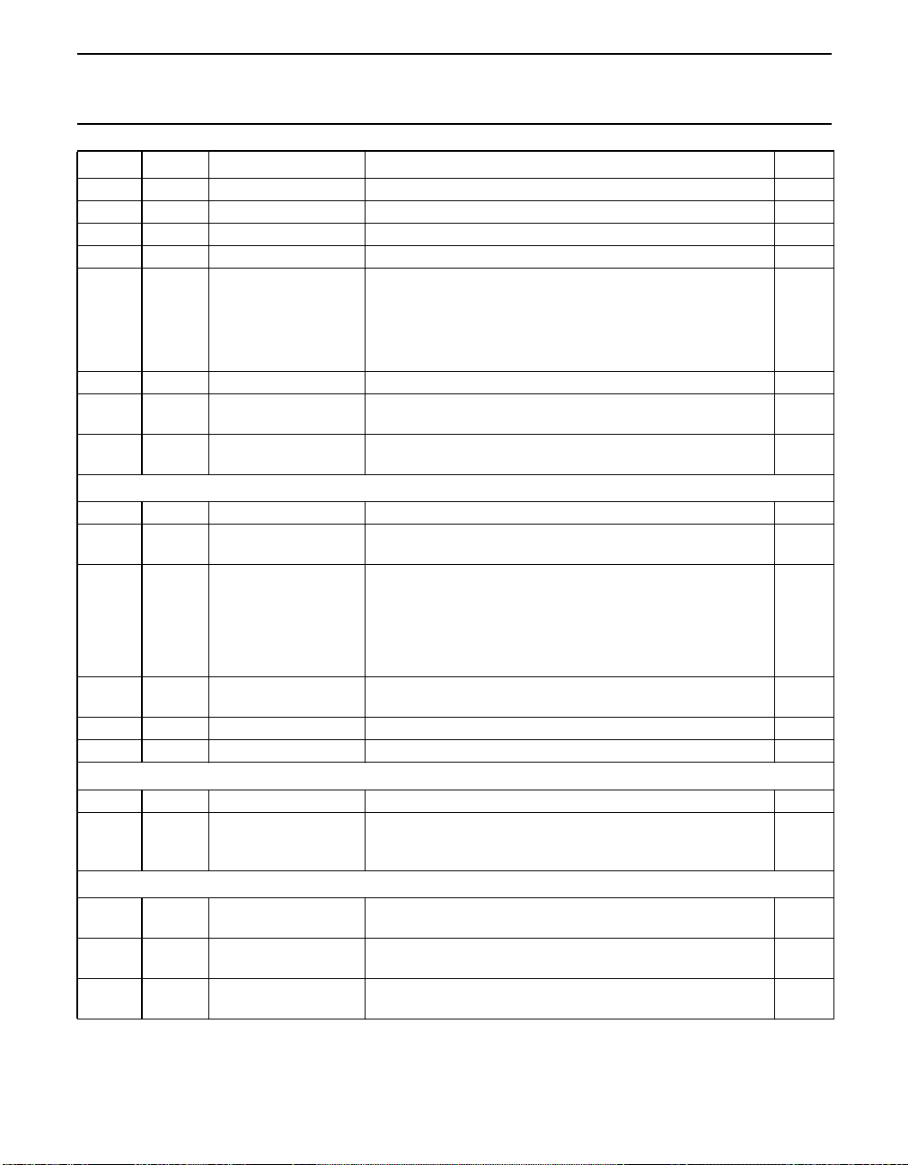
Philips Semiconductors Product specification
Advanced modem/audio analog front-end UCB1300
BIT MODE SYMBOL REMARK RESET
4 R/W TSMX_GND If ‘1’, the TSMX pin is grounded. 0
5 R/W TSPX_GND If ‘1’, the TSPX pin is grounded. 0
6 R/W TSMY_GND If ‘1’, the TSMY pin is grounded. 0
7 R/W TSPY_GND If ‘1’, the TSPY pin is grounded. 0
8 and 9 R/W TSC_MODE[n] Touch screen operation mode: 0
00: interrupt mode
01: pressure measurement mode
1x: position measurement mode.
11 R/W TSC_BIAS_ENA If ‘1’, the touch screen bias circuit is activated. 0
12 R TSPX_LOW This bit returns the inverted state of the TSPX pin, ‘0’ is a high
voltage (pen up), ‘1’ is a low voltage (pen down).
13 R TSMX_LOW This bit returns the inverted state of the TSMX pin, ‘0’ is a high
voltage (pen up), ‘1’ is a low voltage (pen down).
Address 10: ADC control register
0 R/W ADC_SYNC_ENA If ‘1’, the ADC sync mode is activated.
1 R/W VREFBYP_CON If ‘1’, the internal reference voltage is connected to VREFBYP
(pin 16).
2 to 4 R/W ADC_INPUT[n] ADC input select: 0
000: TSPX 100: AD0
001: TSMX 101: AD1
010: TSPY 110: AD2
011: TSMY 110: AD3
5 R/W EXT_REF_ENA If ‘1’, an external reference voltage has to be applied to
VREFBYP.
7 R/W ADC_START A 0-to-1 transition starts the ADC conversion sequence. 0
15 R/W ADC_ENA If ‘1’, the ADC circuit is activated. 0
Address 11: ADC data register
5 to 14 R ADC_DATA[n] Returns the ADC result 0
15 R ADC_DAT_VAL Returns '0' if an ADC conversion is in progress. Returns '1' if
the ADC conversion is completed and the ADC data is stored
in the ADC_DATA[n] register.
Address 12: ID register
0 to 5 R VERSION[n] Returns 0001010 for all the UCB1300 circuits meeting this
specification
6 to 11 R DEVICE[n] Returns 000000 for all the UCB1300 circuits meeting this
specification
12 to 15 R SUPPLIER[n] Returns 0001 for all the UCB1300 circuits meeting this
specification
0
0
0
0
0
0
0
2000 Jun 26 52
Page 53
Philips Semiconductors Product specification
Advanced modem/audio analog front-end UCB1300
BIT MODE SYMBOL REMARK RESET
Address 13: MODE register; note 1
0 R/W AUD_TEST If ‘1’, the analog audio test mode is activated.
1 R/W TEL_TEST If ‘1’, the analog telecom test mode is activated.
2 to 5 R/W PROD_TEST_MODE These bits select the built-in production test modes.
12 R/W DYN_VFLAG_ENA If ‘1’, the dynamic data valid flag mode is activated for both the
audio and the telecom data valid flag.
13 R/W AUD_OFF_CAN If ‘1’ the offset cancelling circuit in the audio path is enabled 0
14 R/W A_BIG_ENDIAN ‘1’-> big endian for audio samples 0
15 R/W T_BIG_ENDIAN ‘1’-> big endian for telecom samples 0
Address 14: Reserved
Reserved for future use.
Address 15: NULL register
0 to 15 R Returns [1111111111111111] at all times
Notes
1. Activating one or more test modes changes the functionality of the UCB1300.
2. TEST (pin 13) must be HIGH when writing to these bits.
(2)
(2)
(2)
0
0
0
0
2000 Jun 26 53
Page 54
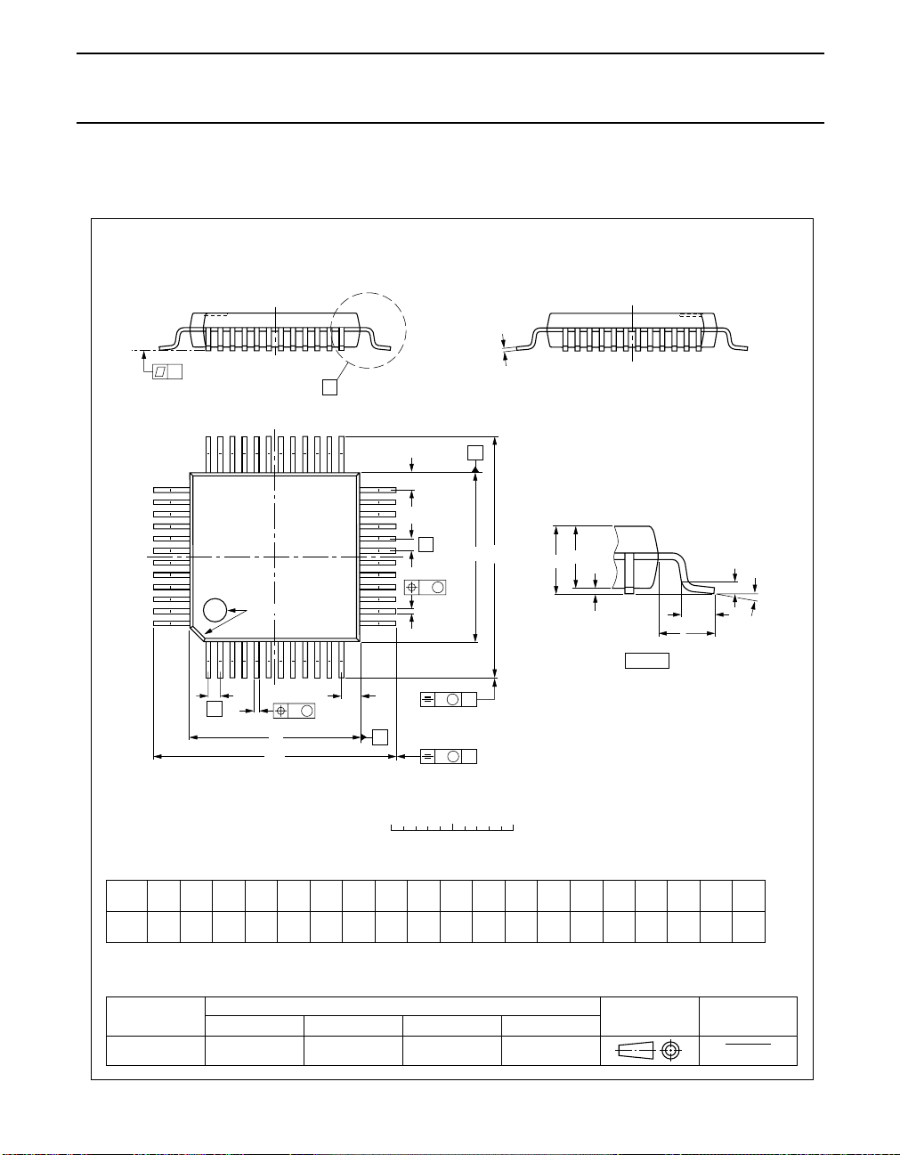
Philips Semiconductors Product specification
Advanced modem/audio analog front-end UCB1300
PACKAGE OUTLINES
LQFP48: plastic low profile quad flat package; 48 leads; body 7 x 7 x 1.4 mm
c
48
y
36
37
pin 1 index
1
e
b
p
D
H
X
25
Z
24
E
b
13
12
Z
w M
D
D
B
e
w M
p
v M
v M
A
H
E
E
A
B
A
A
SOT313-2
2
A
1
detail X
(A )
3
L
p
L
θ
0 2.5 5 mm
scale
DIMENSIONS (mm are the original dimensions)
Note
1. Plastic or metal protrusions of 0.25 mm maximum per side are not included.
A
UNIT
mm
OUTLINE
VERSION
SOT313-2 MS-026136E05
A1A2A3bpcE
max.
0.20
0.05
1.45
1.35
1.60
(1)
(1) (1)(1)
D
0.18
0.12
7.1
6.9
REFERENCES
0.27
0.25
0.17
IEC JEDEC EIAJ
eHELL
7.1
0.5
6.9
2000 Jun 26 54
H
9.15
8.85
Zywv θ
EUROPEAN
Z
0.95
0.55
D
E
0.95
7
0.55
0
ISSUE DATE
99-12-27
00-01-19
o
o
0.75
0.45
p
0.12 0.10.21.0
PROJECTION
D
9.15
8.85
Page 55

Philips Semiconductors Product specification
Advanced modem/audio analog front-end UCB1300
SOLDERING
Introduction
There is no soldering method that is ideal for all IC packages. Wave soldering is often preferred when through-hole and
surface mounted components are mixedon one printed-circuitboard. However, wavesoldering is not always suitable for
surface mounted ICs, or for printed-circuits with high population densities. In these situations reflow soldering is often
used.
This textgives a very briefinsight to a complextechnology. A more in-depthaccount of soldering ICscan be found inour
“IC Package Databook”
Reflow soldering
Reflow soldering techniques are suitable for all LQFP packages.
Reflow soldering requiressolder paste (a suspension of fine solderparticles, flux and binding agent) to be applied to the
printed-circuit board by screen printing, stencilling or pressure-syringe dispensing before package placement.
Several techniques exist for reflowing; for example, thermal conduction by heated belt. Dwell times vary between
50 and 300 seconds depending on heating method. Typical reflow temperatures range from 215 to 250 °C.
Preheating is necessary to dry the paste and evaporate the binding agent. Preheating duration: 45 minutes at 45 °C.
Wave soldering
Wave soldering is not recommended for LQFP packages. This is because of the likelihood of solder bridging due to
closely-spaced leads and the possibility of incomplete solder penetration in multi-lead devices.
If wave soldering cannot be avoided, the following conditions must be observed:
• A double-wave (a turbulent wave with high upward pressure followed by a smooth laminar wave) soldering
technique should be used.
• The footprint must be at an angle of 45° to the board direction and must incorporate solder thieves
downstream and at the side corners.
Even with these conditions, do not consider wave soldering LQFP packages LQFP48 (SOT313-2),
LQFP64 (SOT314-2) or LQFP80 (SOT315-1).
During placement and before soldering, the package must be fixed with a droplet of adhesive. The adhesive can be
applied by screen printing, pin transfer or syringe dispensing. The package can be soldered after the adhesive is cured.
Maximum permissible solder temperature is 260 °C, and maximum duration of package immersion in solder is
10 seconds, if cooled to less than 150 °C within 6 seconds. Typical dwell time is 4 seconds at 250 °C.
A mildly-activated flux will eliminate the need for removal of corrosive residues in most applications.
(order code 9398 652 90011).
Repairing soldered joints
Fix the component by first soldering two diagonally- opposite end leads. Use only a low voltage soldering iron (less
than 24 V) applied to the flat part of the lead. Contact time must be limited to 10 seconds at up to 300 °C. When using a
dedicated tool, all other leads can be soldered in one operation within 2 to 5 seconds between 270 and 320 °C.
2000 Jun 26 55
Page 56
Philips Semiconductors Product specification
Advanced modem/audio analog front-end UCB1300
DEFINITIONS
Data sheet status
Objective specification This data sheet contains target or goal specifications for product development.
Preliminary specification This data sheet contains preliminary data; supplementary data may be published later.
Product specification This data sheet contains final product specifications.
Limiting values
Limiting values given are in accordance with the Absolute Maximum Rating System (IEC 134). Stress above one or
more of the limiting values may cause permanent damage to the device. These are stress ratings only and operation
of the device at these or at any other conditions above those given in the Characteristics sections of the specification
is not implied. Exposure to limiting values for extended periods may affect device reliability.
Application information
Where application information is given, it is advisory and does not form part of the specification.
LIFE SUPPORT APPLICATIONS
These products are not designed for use in life support appliances, devices, or systems where malfunction of these
products can reasonably be expected to result in personal injury. Philips customers using or selling these products for
use in such applications do so at their own risk and agree to fully indemnify Philips for any damages resulting from such
improper use or sale.
RIGHT TO MAKE CHANGES
Philips Semiconductors reserves the right to make changes, without notice, in the products, including circuits, standard
cells, and/or software, described or contained herein in order to improve design and/or performance. Philips
Semiconductors assumes no responsibility or liability for the use of any of these products, conveys no license or title
underany patent, copyright,or maskwork right tothese products,and makes norepresentations orwarranties that these
products are free from patent, copyright, or mask work right infringement, unless otherwise specified.
Philips Semiconductors
811 East Arques Avenue
P.O. Box 3409
Sunnyvale, California 94088-3409
Telephone 800-234-7381
Document order number: 9397-750-07259
@ Copyright PHilips Electronics North America Corporation 2000
All rights reserved. Printed in U.S.A.
Date of release: 06-00
2000 Jun 26 56
 Loading...