

Page 1

INTEGRATED CIRCUITS
UCB1100
Advanced modem/audio analog front-end
Preliminary specification
Supersedes data of 1996 Apr 09
Version 1.2
1998 May 08
Page 2

Philips Semiconductors Preliminary specification
UCB1 100Advanced modem/audio analog front-end
Version 1.2
GENERAL DESCRIPTION
The UCB1100 is a single chip, integrated mixed signal audio and
telecom codec. The single channel audio codec is designed for
direct connection of a microphone and speaker. The built-in telecom
codec can directly be connected to a DAA and supports high speed
modem protocols. The incorporated 10 bit analogue to digital
converter and the touch screen interface provides complete control
and readout of a connected 4 wire resistive touch screen. The 10
additional general purpose I/O pins provides programmable inputs
and/or outputs to the system.
The UCB1100 has a serial interface bus (SIB) intended to
communicate to the system controller. Both the codec input and
output data and the control register data is multiplexed on this SIB
interface.
APPLICATIONS
•Personal Intelligent Communicators
•Personal Digital Assistants (PDA)
•Screen phones
•Smart Phone and smart Fax
•Intelligent Communicators
KEY FEATURES
•48-pin LQFP (SOT313-2) small body SMD package and low
external component count result in minimal PCB space
requirement.
•A 12-bit sigma delta audio codec with programmable sample rate,
input and output voltage levels, capable of connecting directly to
speaker and microphone, including digitally controlled mute,
loopback and clip detection functions
•A 14-bit sigma delta telecom codec with programmable sample
rate, including digitally controlled input voltage level, mute,
loopback and clip detection functions. The telecom codec is
intended for direct connection to a DAA (digital access
arrangement) and includes a built-in sidetone suppression circuit.
•A complete 4 wire resistive touch screen interface circuit
supporting position, pressure and plate resistance measurements.
•A 10-bit successive approximation ADC with internal track and
hold circuit and analogue multiplier for touch screen readout and
monitoring of four external high voltage (7.5V) analogue voltages.
•A high speed, 4 wire serial interface data bus (SIB) for
communication to system controller.
•A 3.3V supply voltage and built in power saving modes make the
UCB1100 optimal for portable and battery powered applications.
T ABLE OF CONTENTS
GENERAL DESCRIPTION 2. . . . . . . . . . . . . . . . . . . . . . . . . . . . . . . . .
APPLICATIONS 2. . . . . . . . . . . . . . . . . . . . . . . . . . . . . . . . . . . . . . . . . . .
KEY FEATURES 2. . . . . . . . . . . . . . . . . . . . . . . . . . . . . . . . . . . . . . . . . .
TABLE OF CONTENTS 2. . . . . . . . . . . . . . . . . . . . . . . . . . . . . . . . . . . .
1.0 FUNCTIONAL BLOCK DIAGRAM 3. . . . . . . . . . . . . . . . . . . . .
2.0 ORDERING INFORMATION 4. . . . . . . . . . . . . . . . . . . . . . . . . .
3.0 ABSOLUTE MAXIMUM RATINGS 4. . . . . . . . . . . . . . . . . . . . .
4.0 DC ELECTRICAL CHARACTERISTICS 5. . . . . . . . . . . . . . . .
5.0 PINOUT 6. . . . . . . . . . . . . . . . . . . . . . . . . . . . . . . . . . . . . . . . . . . .
5.1 PINLIST 7. . . . . . . . . . . . . . . . . . . . . . . . . . . . . . . . . . . . . .
6.0 FUNCTIONAL DESCRIPTION 8. . . . . . . . . . . . . . . . . . . . . . . .
6.1 AUDIO CODEC 8. . . . . . . . . . . . . . . . . . . . . . . . . . . . . . .
6.1.1 AUDIO INPUT SPECIFICATIONS 10. . . . . . . .
6.1.2 AUDIO OUTPUT SPECIFICATIONS 11. . . . . . .
6.2 TELECOM CODEC 12. . . . . . . . . . . . . . . . . . . . . . . . . . .
6.2.1 TELECOM INPUT SPECIFICATIONS 14. . . . .
6.2.2 TELECOM OUTPUT SPECIFICATIONS 15. . .
6.3 TOUCH SCREEN MEASUREMENT MODES 16. . . .
6.3.1 POSITION MEASUREMENT 16. . . . . . . . . . . . .
6.3.2 PRESSURE MEASUREMENT 16. . . . . . . . . . .
6.3.3 PLATE RESISTANCE MEASUREMENT 16. . .
6.4 TOUCH SCREEN INTERFACE 17. . . . . . . . . . . . . . . . .
6.4.1 TOUCH SCREEN SPECIFICATIONS 18. . . . .
6.5 10 BIT ADC. 19. . . . . . . . . . . . . . . . . . . . . . . . . . . . . . . . .
6.5.1 SPECIFICATION OVERVIEW 21. . . . . . . . . . . .
6.6 ON CHIP REFERENCE CIRCUIT 21. . . . . . . . . . . . . .
6.6.1 SPECIFICATION OVERVIEW 21. . . . . . . . . . . .
6.7 SERIAL INTERFACE BUS 22. . . . . . . . . . . . . . . . . . . . .
6.7.1 SIB DATA FORMAT 23. . . . . . . . . . . . . . . . . . . . .
6.7.2 CODEC DATA TRANSFER 24. . . . . . . . . . . . . .
6.7.3 CONTROL REGISTER DATA TRANSFER 26.
6.7.4 AC ELECTRICAL CHARACTERISTICS 27. . .
6.8 GENERAL PURPOSE I/Os 27. . . . . . . . . . . . . . . . . . . .
6.9 INTERRUPT GENERATION 27. . . . . . . . . . . . . . . . . . .
6.10 RESET CIRCUITRY 28. . . . . . . . . . . . . . . . . . . . . . . . . .
7.0 MISCELLANEOUS 29. . . . . . . . . . . . . . . . . . . . . . . . . . . . . . . . .
7.1 POWER ROUTING STRATEGY 29. . . . . . . . . . . . . . . .
8.0 CONTROL REGISTER OVERVIEW 30. . . . . . . . . . . . . . . . . .
9.0 PACKAGE OUTLINES 34. . . . . . . . . . . . . . . . . . . . . . . . . . . . . .
9.1 PACKAGE OUTLINE LQFP48 34. . . . . . . . . . . . . . . . . .
10.0 DEFINITIONS 36. . . . . . . . . . . . . . . . . . . . . . . . . . . . . . . . . . . . .
1998 May 08
2
Page 3
Philips Semiconductors Preliminary specification
UCB1 100Advanced modem/audio analog front-end
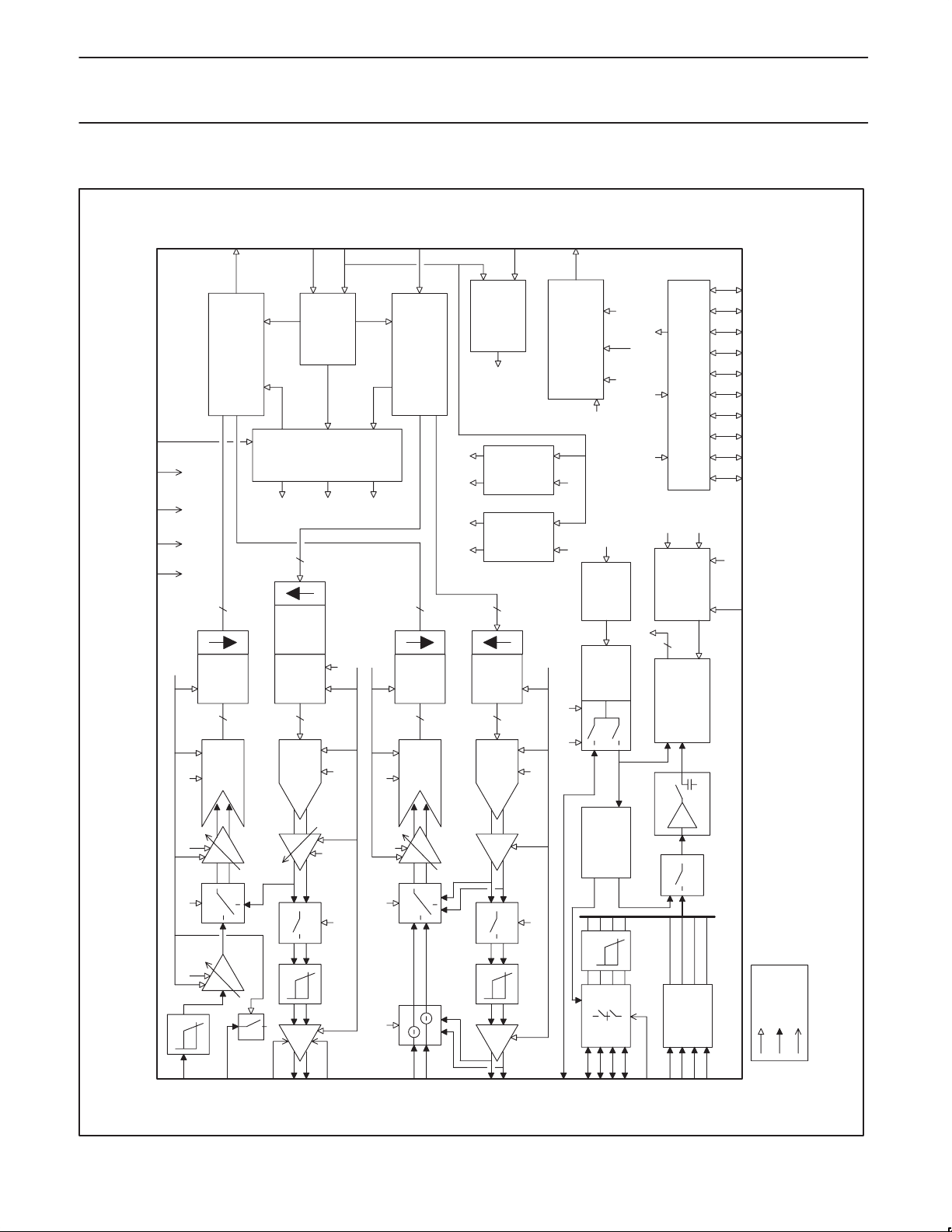
1.0 FUNCTIONAL BLOCK DIAGRAM
test
2xVddd2xVssdVdda1Vssa1
audio_input_enable
sibdout
encoder
serial bus
control data registers
to all other analog and digital blocks
fs
12
fs
12
noise
digital
filter
digital
decimation
1
64fs
digital
volume
64fs
4
sibsync
serial bus
shaper
control
sibclk
controller
serial bus
telecom input enable
audio_output_enable
attn[4,5]
sibdin
fs
14
digital
decimation
4
64fs
decoder
filter
fst 64fst
fsa 64fsa
reset
internal
fs
digital
64fs
reset
14
noise
shaper
4
nreset
stretcher
sample
frequency
sample
frequency
divider
divider
irqout
clear_interrupt[0:15]
Interrupt
controller
rising_edge_ena[0:15]
interrupt data
from other blocks
divtel0:6]
eanble data
for all
analog blocks
divaud[0:6]
power
control
telecom output enable
voltage
reference
external
filter
falling_edge_ena[0:15]
Programmable IO pin block
IOmode[0:9] IOwdat[0:9] IOrdat[0:9]
adc
start
sync
enable
stop logic
ADC start
10
to external register 11
10 bit ADC
io0 io1 io2 io3 io4 io5 io6 io7 io8 io9
adc_sync_ena
adcsync
1998 May 08
64fsa
gain[0,2]
loopback
gain[3,4]
micp
mux
1 bit ADC
micgnd
4 bit DAC
AUDIO CODEC
attn[0,3]
vssa1
spkrp
spkrn
vdda2
vssa2
external
reference
64fsa
effect
mute
echo on loopback
side tone suppression
1 bit ADC
attenuation
mux
tinp
TELECOM CODEC
tinn
4 bit DAC
toutp
toutn
effect
mute
vrefbyp
Figure 1. Block Diagram of the UCB1100
3
bias voltage
touch screen
touch screen
switch matrix
tspy
tsmx
tsmy
vssa3
mux
switched
ad0
ad1
track & hold
9 to 1
voltage
dividers
ad2
ad3
analog pin
digital pin
SN00126
supply pin
Page 4
Philips Semiconductors Preliminary specification
Á
Á
Á
Á
Á
Á
UCB1 100Advanced modem/audio analog front-end
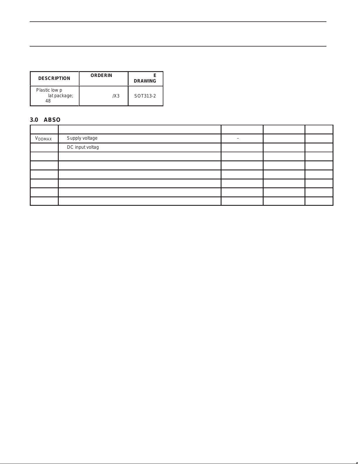
2.0 ORDERING INFORMATION
DESCRIPTION
ÁÁÁÁ
ORDERING
БББББ
CODE
Plastic low profile
quad flat package;
ÁÁÁÁ
48 leads
UCB1100LP/X3
БББББ
3.0 ABSOLUTE MAXIMUM RATINGS
SYMBOL PARAMETER MIN MAX UNIT
V
DDMAX
V
IMAX
V
ADMAX
V
OMAX
I
IKMAX
I
OKMAX
I
OLMAX
T
stg
NOTES:
1. Stresses above those listed under Absolute Maximum Ratings may cause permanent damage to the device. This is a stress rating only and
functional operation of the device at these or any conditions other than those described in the Absolute Maximum Rating section of this
specification is not implied.
2. This product includes circuitry specially designed for the protection of its internal devices from damaging ef fects of excessive static charge.
Nonetheless, it is suggested that conventional precautions be taken to avoid submitting the UCB1100 to conditions exceeding the maximum
ratings.
3. Parameters are valid over the operating ambient temperature unless otherwise specified. All voltages are with respect to the V
unless otherwise noted.
Supply voltage –0.5 5.0 V
DC input voltage, except AD0–3 inputs –0.5 VDD+0.5 V
DC input voltage AD0–3 inputs –0.5 8.5 V
DC output voltage –0.5 VDD+0.5 V
DC diode input current, all inputs 10 mA
DC diode output current 10 mA
Continuous output current, digital outputs 4 mA
Storage temperature –55 150 °C
PACKAGE
ÁÁÁ
DRAWING
SOT313-2
ÁÁÁ
SSD
pin,
1998 May 08
4
Page 5
Philips Semiconductors Preliminary specification
SYMBOL
PARAMETER
NOTES
UNIT
UCB1 100Advanced modem/audio analog front-end
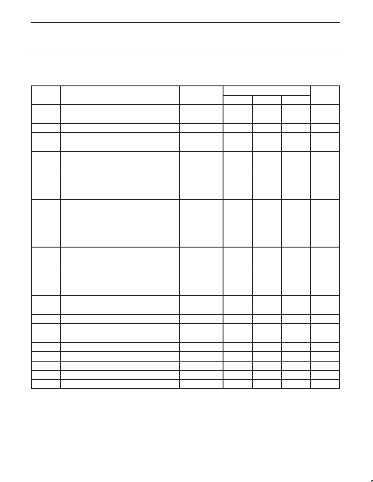
4.0 DC ELECTRICAL CHARACTERISTICS
T
= 0°C to 70°C, V
amb
Voltage with respect to the V
V
DDD
V
DDA1
V
DDA2
V
SSA2
V
SSA3
I
DDD
I
DDA1
I
DDA2
V
TSCB
I
TSCB
V
ADFS
V
TSFS
V
IL
V
IH
V
OL
V
OH
f
SIBCLK
T
amb
NOTES:
1. Indicative value only. Value will be frozen following silicon measurements.
2. Excluding connected touch screen and speaker load currents.
SSD
= V
= V
SSA1
pin, unless otherwise specified.
SSD
SSA2
= V
= 0V , sibclk = 10MHz, audio_divisor = 12, telecom_divisor = 40.
SSA3
LIMITS
MIN TYP MAX
digital supply voltage 3.0 3.3 3.6 V
analogue supply voltage (excl.speaker driver) 3.0 3.3 3.6 V
analogue supply voltage (speaker driver only) 3.0 3.3 3.6 V
analogue ground voltage wrt. V
analogue ground voltage wrt V
digital supply current,
SSD
SSD
Note 1
–0.4 0 0.4 V
–0.4 0 0.4 V
full functionality 19 mA
only audio codec activated 17 mA
only telecom codec activated 19 mA
only touch screen activated 15 mA
only adc activated 15 mA
no functions activated, sibclk stopped 10 µA
analogue supply current,
Note 1, Note 2
full functionality 3.8 mA
only audio codec activated 1.5 mA
only telecom codec activated 1.7 mA
only touch screen activated 0.4 mA
only adc activated 0.5 mA
no analogue functions activated <10 µA
total speaker driver supply current
Note 1, Note 2
full functionality 0.2 mA
only audio codec activated 0.2 mA
only telecom codec activated 10 µA
only touch screen activated 10 µA
only adc activated 10 µA
no analogue functions activated 10 µA
touch screen bias voltage 1.8 V
maximum touch screen bias current 10 mA
full scale voltage ad0–ad3 inputs 7.5 V
full scale input touch screen inputs 7.5 V
input low voltage –0.5 0.3*V
input high voltage 0.7*V
DDD
V
DDD
output low voltage IOL=2mA 0.2*V
output high voltage IOH=2mA 0.8*V
DDD
DDD
+0.5 V
DDD
V
V
V
clock frequency 0 10 15 MHz
Operating Ambient Temperature 0 70 °C
1998 May 08
5
Page 6

Philips Semiconductors Preliminary specification
UCB1 100Advanced modem/audio analog front-end
5.0 PINOUT
vddd
io6
io5
io4
not used
irqout
sibdin
sibclk
sibdout
sibsync
nreset
vssd
adcsync
vssd
not used
vssa2
spkrn
sprkp
vdda2
toutp
toutn
io7
io8
io9
4847464544434241403938
1
2
3
4
5
6
7
8
9
10
11
12
UCB1100
LQFP48
TOP VIEW
37
36
io3
35
io2
34
io1
33
io0
32
vddd
31
not used
30
tspx
29
tsmy
28
tsmx
27
tspy
26
vssa3
25
ad0
1314151617181920212223
test
tinn
tinp
vrefbyp
vdda1
vssa1
not used
micgnd
micp
ad3
Figure 2. LQFP48 (SOT313-2)
ad2
24
ad1
SN00127
1998 May 08
6
Page 7

Philips Semiconductors Preliminary specification
SYMBOL
PIN TYPE
DESCRIPTION
NOTE
UCB1 100Advanced modem/audio analog front-end
5.1 Pinlist
PINNING
LQFP48
vddd 32, 48 supply digital supply
vssd 5, 37 ground digital ground 1
vdda1 17 supply analogue supply
vssa1 18 ground analogue ground 1
vdda2 10 supply analogue speaker driver supply
vssa2 7 ground analogue speaker driver ground
vssa3 26 ground touch screen switch matrix ground
sibclk 41 CMOS input SIB serial interface master clock
sibdin 42 CMOS input SIB data input
sibdout 40 CMOS output ‘0’ / Hi-Z SIB data output 2
sibsync 39 CMOS input SIB synchronization
irqout 43 CMOS output
micp 21 analogue input Hi-Z microphone signal input
micgnd 20 analogue input Hi-Z microphone ground switch input
sprkp 9 analogue output Hi-Z positive speaker output 3
spkrn 8 analogue output Hi-Z negative speaker output 3
tinp 15 analogue input Hi-Z positive telecom codec input 3
tinn 14 analogue input Hi-Z negative telecom codec input 3
toutp 11 analogue output Hi-Z positive telecom codec output 3
toutn 12 analogue output Hi-Z negative telecom codec output 3
ad0–3 25–22 analogue input Hi-Z analogue high voltage inputs
tspx 30 analogue IO Hi-Z positive X-plate touch screen
tsmx 28 analogue IO Hi-Z negative X-plate touch screen
tspy 27 analogue IO Hi-Z positive Y-plate touch screen
tsmy 29 analogue IO Hi-Z negative Y-plate touch screen
adcsync 4 digital input adc synchronization pulse input
vrefbyp 16 analogue IO Hi-Z external reference voltage input, external filter connection
io0–9 33–36,
45–47,
1–3
nreset 38 CMOS input
test 13 CMOS input ‘0’ test mode protection 4
not used 6, 19,
31, 44
NOTES:
1. The vssd and vssa1 pins are connected to each other within the UCB1100.
2. The first 64 bits of the sib frame will be ‘0’, the remaining bits in the sib frame will be Hi-Z.
3. The spkrp/spkrn, tinp/tiln and toup/toutn are dif ferential pairs.
4. The test pin contains a internal pull down. This pin should be connected to vssd in normal mode of the UCB1100.
active-High
CMOS IO input general purpose IO pins
active-Low
RESET
STATE
‘0’ interrupt output
asynchronous reset input
not connected pins
1998 May 08
7
Page 8
Philips Semiconductors Preliminary specification
UCB1 100Advanced modem/audio analog front-end
6.0 FUNCTIONAL DESCRIPTION
The UCB1100 consists of several analogue and digital sub circuits
which can be programmed via the Serial Interface Bus (SIB). This
enables the user to set the UCB1100 functionality according actual
application requirements.
6.1 Audio codec
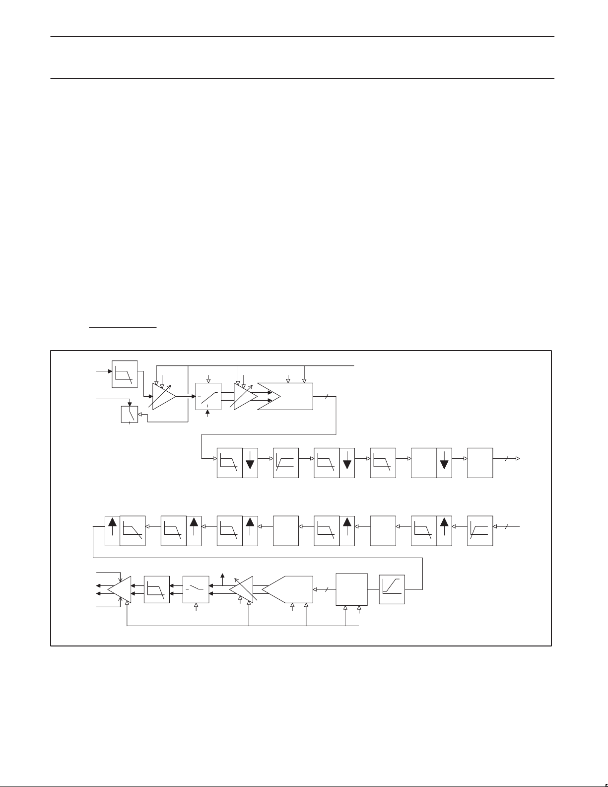
The audio codec contains an input channel, built up from a 64 times
oversampling sigma delta analogue to digital converter (ADC) with
digital decimation filters and a programmable gain microphone
preamp. The output path consists of a digital up sample filter, a 64
time oversampling 4 bit digital to analogue converter (DAC) circuit
followed by a speaker driver, capable of driving directly a low
impedance bridge tied (BTL) speaker. The output path features
digitally programmable attenuation and a mute function. The audio
codec also incorporates a loopback mode, in which codec output
path and the input path are connected in series.
The audio sample rate is derived from the SIB interface clock pin
(SIBclk) and is programmable through the SIB interface. The audio
sample rate is given by the following equation:
(2 *
Fsibclk
Fsa
micp
micgnd
audio_divisor
(64 *
)
(5
)
gain[3,4]
audio_divisor
loopback
mux
128)
gain[0,2]
64fsa
1 bit ADC
For example, a serial clock of 10 MHz, with a divisor of 14, results in
an audio sample rate of 22.321kHz. Both the rising and the falling
edges of the sibclk are used in case an odd audio_divisor is set.
Thus a 50% duty cycle of the sibclk signal is mandatory to obtain
time equidistant sampling with odd divisors.
The frequency response of the audio codec depends mainly on the
selected sample rate, since the bandwidth is limited in the down and
up sampling filters. These digital filters both contain several FIR and
IIR low pass filters and a DC removal filter (high pass filter). A 1st
order analogue anti aliasing filter is implemented at the input of the
microphone input to prevent aliasing in the adc path. A 3rd order
smoothing filter is implemented between dac and speaker driver
stage to reduce the spurious frequencies at the speaker outputs.
The audio codec input (=ADC) and output (= DAC) paths can be
enabled individually by setting the audio_adc and/or audio_dac bits
in the audio control register B. These enable bits operate both on
the associated analogue and digital functions, for optimal power
control of both the analogue and the digital parts.
audio_input_enable
64fs
1
vdda2
spkrp
spkrn
vssa2
vssa1
interpolator
4
low pass
FIR
loop input
16
2
mute
Sinc4
FIR
half band
FIR
loop input
attn[0,3]
2
DC
removal
round
up
4 bit DAC
64fsa
half band
WDF
half band
WDF
64fs
4
Figure 3. Detailed Block Diagram Audio codec
2
2
digital
volume
control
attn[4,5]
audio_output_enable
half band
WDF
+3dB
noise
shaper
+3dB
round
2
DC
removal
2
fs
12
up
fs
12
SN00128
1998 May 08
8
Page 9

Philips Semiconductors Preliminary specification
UCB1 100Advanced modem/audio analog front-end
UCB1100 UCB1100
vdda1
micp
micgnd
vssa1
vdda1
micp
micgnd
vssa1
‘Passive’ Microphone ‘Active’ Microphone
SN00129
Figure 4. Possible Microphone Connections
The UCB1100 audio codec input path accepts microphone signals
directly, only a DC blocking capacitor is needed, since the micp input
is biased around 1.4V . The ‘ground’ side of the microphone is either
connected to the analogue ground (vssa1) or to the micgnd pin of
the UCB1100. The latter will decrease the current consumption of
active microphones, since the micgnd pin is made Hi-Z when the
audio codec input path is disabled.
The full scale input voltage of the audio input path is programmable
in 1.5dB steps by setting the appropriate data in the
audio-input-gain
bits in the audio control register A.
A clip detection circuit will inform the user whenever the input
voltage exceeds the maximum input voltage. In that case the
detect status
bit in audio control register B is set. An interrupt is
generated on the irqout pin of the UCB1100 whenever the
clip detect rising interrupt
audio
edge interrupt
bit is set in the rising edge interrupt enable or falling
or the
enable audio detect falling
clip
enable
edge interrupt control register B is set.
48dB
24dB
digital attenuation
0dB
21dB
analog attenuation
0dB
24dB 48dB 69dB
programmed attenuation
SN00130
Figure 5. Analogue and Digital Attenuation Settings
Audio Output Path
The output level can be attenuated in 3dB steps down to -69dB. The
8 highest attenuation steps are implemented in the analogue
circuitry, while the two 24dB steps are implemented in the digital
domain. This preserves the ‘audio quality’ of the output signal at
lowest attenuation settings. The speaker driver is muted when the
audio-mute
bit in the audio control register B is set. The speaker
driver will remain activated in that case, however no signal is
produced by the speaker driver circuitry.
UCB1100 UCB1100 UCB1100
spkrp
spkrn
Bridge Tied
spkrp spkrp
spkrn spkrn
Single Ended Speaker Connections
Speaker
Load
SN00131
Figure 6. Possible Speaker Connections
The speaker driver is designed to directly drive a bridge tied load
(BTL). This yields the highest output power and it does not require
external DC blocking capacitors. The speaker driver also accepts
single ended connection of a speaker, in which case the maximum
output power is reduced to a quarter of the BTL situation.
Consequently this way of connecting the speaker to the speaker
driver reduces the power consumption of the speaker driver in the
UCB1100 by a factor of 2. Figure 6 shows possible ways to connect
a speaker to the UCB1100.
The audio input and output path are activated independently; the
input path is enabled when the
output path is enabled when the
audio-input-enable
audio-output-enable
bit is set, the
bit is set in the
audio control register B. This provides the user the means to reduce
the current consumption of the UCB1100 if one part of the audio
codec is not used in the application.
The audio codec has a loopback mode for system test purposes,
which is activated when the
audio_loopback enable
bit in the audio
control register B is set. This is an analogue loopback which
internally connects the output of the audio output path to the input of
the audio input path, (see Figure 3). In this mode the normal
microphone input is ignored, but the speaker driver can be operated
normally .
1998 May 08
9
Page 10

Philips Semiconductors Preliminary specification
SYMBOL
PARAMETER
CONDITIONS
UNIT
UCB1 100Advanced modem/audio analog front-end
6.1.1 Audio Input Specifications
LIMITS
MIN TYP MAX
F
SA
V
INAM
V
MICP
R
INPAI
R
HINE
G
SA
N
AGS
G
mA
G
EAR
ROES
AI
DNA
AI
THUD
AI
THD
MGAI
SNR
AI
SNR
MGAI
RIP
IA
SBR
IA
E
IA
NOTE: Coding scheme for ADC output data is 2’s complement.
audio sample frequency 26 kHz
full scale input voltage 0 dB gain setting 0.28 V
pp
DC bias voltage micp input audio input path enabled 1.4 V
input impedance audio input path enabled 25 kΩ
impedance micgnd to vssa1 audio input path enabled 100 Ω
gain step size 1.3 1.5 1.7 dB
number of gain steps 32
maximum gain 46.5 dB
gain error (accuracy of gain setting)
0 dB gain setting,
full scale input voltage
–1 0 1 dB
resolution audio input 12 bit
differential non linearity audio input ADC 0.9 LSB
total harmonic distortion
total harmonic distortion
signal to noise ratio
audio input
signal to noise ratio
pass band ripple F
stop band rejection
audio input
out of band rejection
audio input
0db input gain selected
0.28Vpp, 1kHz to micp
46.5dB gain setting,
1mVpp, 1kHz to micp
0dB input gain selected
0.28Vpp, 1kHz to micp
46.5dB gain selected
1mVpp, 1kHz to micp
<Fsig < F
PLAI
F
<Fsig.<20kHz 70 dB
SHAI
PHAI
65 dB
50 dB
0.03 %
0.1 %
0.5 dB
F > 20kHz t.b.f. mVrms
RIP
IA
0dB
SBR
IA
F
PLA
FREQUENCY (Hz)
Figure 7. Audio Input Path Frequency Response
1998 May 08
F
= 0.00016 * F
PLA
F
= 0.42 * F
PHA
F
= 0.6 * F
SHA
F
F
SHA
PHA
SN00132
SA
SA
SA
10
Page 11
Philips Semiconductors Preliminary specification
SYMBOL
PARAMETER
CONDITIONS
UNIT
UCB1 100Advanced modem/audio analog front-end
6.1.2 Audio Output Specifications
LIMITS
MIN TYP MAX
V
OFFIA
V
OOA
V
OFFOA
V
SPK
A
SOA
NSOA number of attenuation steps 24
A
MOA
ROES
OA
DNA
OA
THUD
OAS
THUD
OAH
SNR
OAS
SNR
OAH
RIP
OA
F
SUOA
SBR
OA
E
IOA
Z
SPKR
NOTE: Coding scheme for DAC input data is 2’s complement.
offset error No signal applied to micp 0 LSB
0dB attenuation,
full scale output voltage
offset error 16ohm speaker 50 mV
DC bias voltage
spkrp and spkrn pin
16ohm speaker
3.2 V
differential Spkrp–Spkrn
Audio output path enabled 1.4 V
pp
pp
attenuation step size 2.8 3.0 3.2 dB
maximum attenuation 69 dB
resolution 12 bit
differential non linearity DAC 0.9 LSB
total harmonic distortion
16Ω speaker
total harmonic distortion
1kΩ headphone
signal to noise ratio
16Ω speaker
signal to noise ratio,
1kHΩ headphone
pass band ripple F
cut off frequency upper stop band 0.6 F
stop band rejection F
0dB attenuation
20Hz to 20kHz
0dB attenuation
20Hz to 20kHz bandwidth
0dB attenuation
20Hz to 20kHz bandwidth
0dB attenuation
20Hz to 20kHz bandwidth
< Fsig <– F
PLAO
<Fsig.<20kHz 70 dB
SHAO
PHAO
0.5 2 %
0.03 %
40 80 dB
65 80 dB
0.5 dB
SA
integrated out of band energy F > 20kHz 30 mVrms
speaker impedance 8 16 Ω
RIP
OA
0dB
SBR
OA
F
PLA
FREQUENCY (Hz)
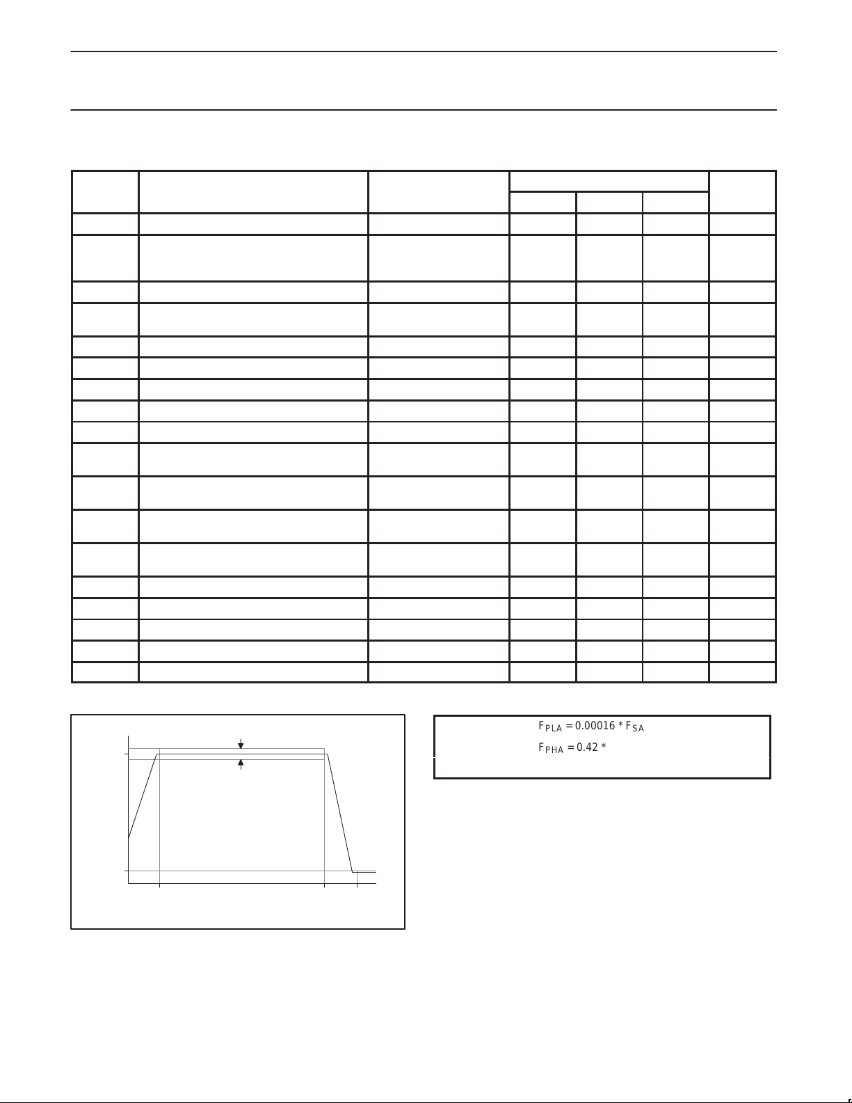
Figure 8. Audio Output Filter Frequency Response
1998 May 08
F
PHA
F
SHA
SN00133
F
= 0.00016 * F
F
F
PLA
PHA
SHA
= 0.42 * F
= 0.6 * F
SA
SA
SA
11
Page 12
Philips Semiconductors Preliminary specification
UCB1 100Advanced modem/audio analog front-end
6.2 Telecom codec
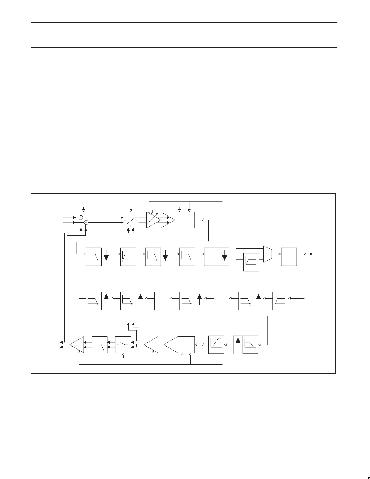
The telecom codec contains an input channel, built up from a 64
times oversampling sigma delta analogue to digital converter (ADC)
with digital decimation filters, programmable attenuation and build in
sidetone suppression circuit. The output path consist of a digital up
sample filter, a 64 time oversampling 4 bit digital to analogue
converter (DAC) circuit followed by a differential output driver,
capable of directly driving a 600ohm isolation transformer. The
output path includes a mute function. The telecom codec also
incorporates a loopback mode, in which codec output path and the
input path are connected in series.
The telecom sample rate is derived from the SIB interface clock pin
(sibclk) and is programmable through the SIB interface. The telecom
sample rate is given by the following formula:
Fsibclk
(64 *
(2 *
telecom_divisor
Fst
For example, a sibclk of 10 MHz, with a divisor of 40, results in a
telecom sample rate of 7.813kHz. Both the rising and the falling
side tone suppression
tinp
tinn
)
(5
)
echo on loopback
telecom_divisor
mux
loop inputs
128)
attenuation
edges of the sibclk are used in case an odd telecom_divisor is set.
In that case a 50% duty cycle of the sibclk signal is mandatory to
obtain time equidistant sampling.
The input path of the telecom codec has a programmable
attenuation. It also implements a voice band filter, which consists of
an digital low pass filter, which is a part of the decimation filter.
Therefore the pass band of the voice band filter is determined by the
selected telecom codec sample rate. This voice band filter is
activated by the
high pass enable
bit in the telecom control register
B. The resulting telecom input filter curves are given in Figures 11
and 12.
The output section of the telecom codec is designed to interface with
a 600 ohm line through an isolation transformer. The built in mute
function is activated by the
mute
bit in the telecom control register B.
The output driver remains active in the mute mode, however no
output signal is produced.
effect
1 bit ADC
64fs
4
telecom input enable
toutp
toutn
Sinc4
FIR
low pass
FIR
fs
14
up
fs
14
SN00134
DC
removal
round
+3dB
16
DC
removal
half band
FIR
2
loop inputs
mute
half band
2
WDF
round
up
2
half band
WDF
half band
FIR
2
4 bit DAC
effect
64fs
4
2
+3dB
noise
shaper
telecom output enable
high pass
half band
FIR
interpolator
4
FIR
2
Figure 9. Detailed Block Diagram Telecom codec
1998 May 08
12
Page 13
Philips Semiconductors Preliminary specification
UCB1 100Advanced modem/audio analog front-end
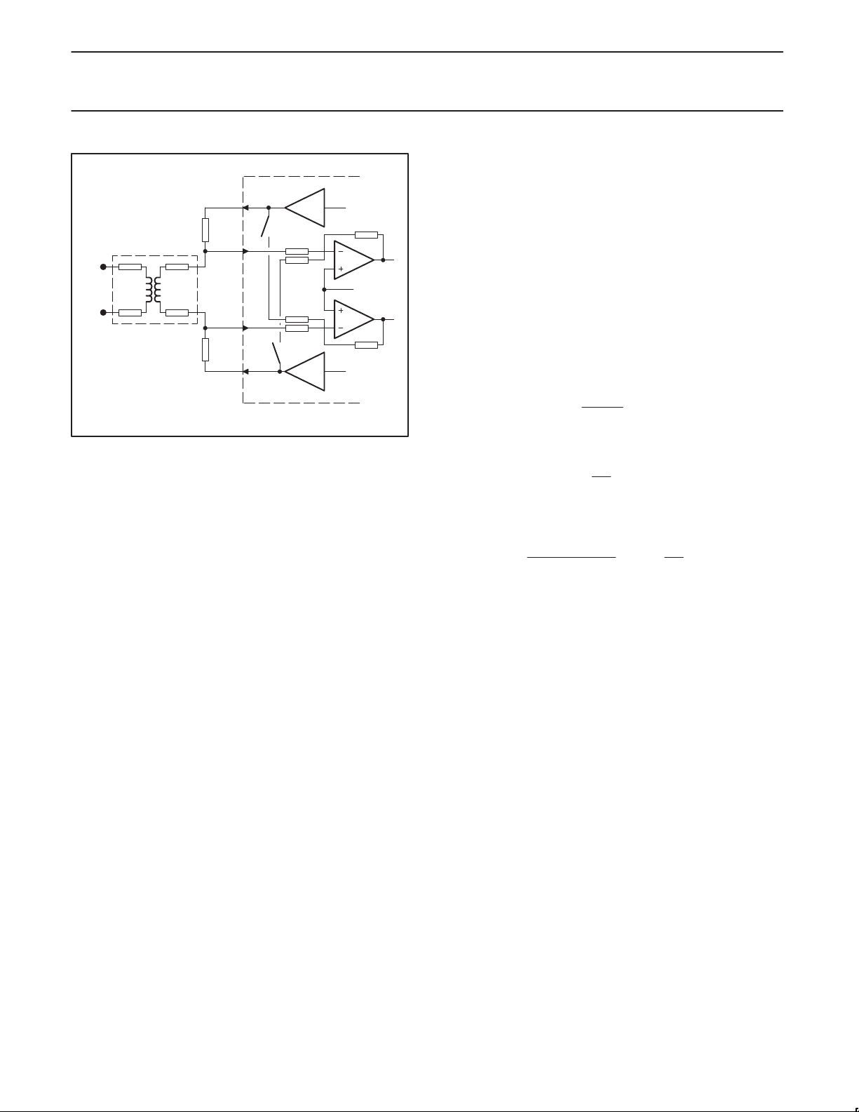
An important built in feature of the telecom codec is the sidetone
suppression circuit. The sidetone suppression circuit is activated
A
B
1:1 transformer
when the
toutp
Ro
tinp
RtRt
Ri
Rs
Rg
register B is set. The telecom input signal contains a large part of
the telecom output signal Tout, when the sidetone suppression
circuit is disabled. The available dynamic range of the telecom input
is occupied largely by the telecom output voltage.
The sidetone suppression circuit subtracts a part of the telecom
output signal from the telecom input signal when activated. The
available dynamic range is in that case used more effectively than
RtRt
tinn
Ro
toutn
Rs
Ri
Rg
without sidetone suppression.
The built in side tone suppression circuit, shown in Figure 9, has a
fixed subtraction ratio, set be the resistors Rs and Ri, which equals
600 / 456. This ratio is calculated from the following relations:
The impedance seen by the telephone line equals:
sidetone suppression enable
bit in the telecom control
SN00135
Figure 10. Telecom codec Sidetone Suppression Circuitry
Shown with the Typical Connection between UCB1100 and
Telephone Line (No Protections Circuits Shown)
Rline
+ 2*
ǒ
Rt)Rt
)
Ro*Ri
Ro
)
Ǔ
Ri
In which Rt represents winding resistance of the transformer, divided
by 2. Assuming Ri >> Ro then
Rline+Rt)Rt)Ro
600
+
+ 300
2
A typical transformer has 156 ohm winding impedance, thus Re
should be 144 ohm. The ratio of the telecom input and output
voltage is therefore
Tin+Tout
156 ) 300
*
156 ) 300 ) 144
+
Tout
*
456
600
1998 May 08
13
Page 14
Philips Semiconductors Preliminary specification
SYMBOL
PARAMETER
CONDITIONS
UNIT
UCB1 100Advanced modem/audio analog front-end
6.2.1 Telecom Input Specifications
LIMITS
MIN TYP MAX
F
ST
V
INTM
V
TIN
A
SIT
N
STI
A
MTI
A
ERTI
R
TI
SINAD
TI
SINAD
TIS
DNL
TI
RES
TI
RIP
TI
RIP
VTI
SBR
VTI
SBR
HTI
S
SUP
NOTE: Coding scheme for ADC output data is 2’s complement.
sample frequency 10 kHz
full scale input voltage 0 dB attenuation setting 0.519 V
DC bias voltage Tinp / Tinn pins telecom input path enabled 1.4 V
attenuation step size 6 dB
number of attenuation steps 2
maximum attenuation 6 dB
attenuation error
(accuracy of attenuation setting)
0 dB attenuation setting,
full scale input voltage
–0.5 0 0.5 dB
input impedance 25 kΩ
total harmonic distortion
+ noise to signal ratio
total harmonic distortion
+ noise to signal ratio
full scale input signal 70 dB
–43dBm input voltage 32 dB
differential non linearity ADC 2 LSB
resolution 14 bit
pass band ripple, no voice filter F
pass band ripple, voice filter activated F
stop band rejection,
voice filter activated
stop band rejection F
PLTI
VHTI
Fsig < F
SHTI
< Fsig < F
< Fsig < F
VLTI
<Fsig.<F
PHTI
PHTI
ST
0.6 dB
0.6 dB
30 dB
55 dB
600Ω line,
sidetone suppression effectiveness
1:1 line transformer with
20 dB
156Ω winding resistance
p
RIP
TI
0dB
SBR
HTI
F
PLT
FREQUENCY (Hz)
F
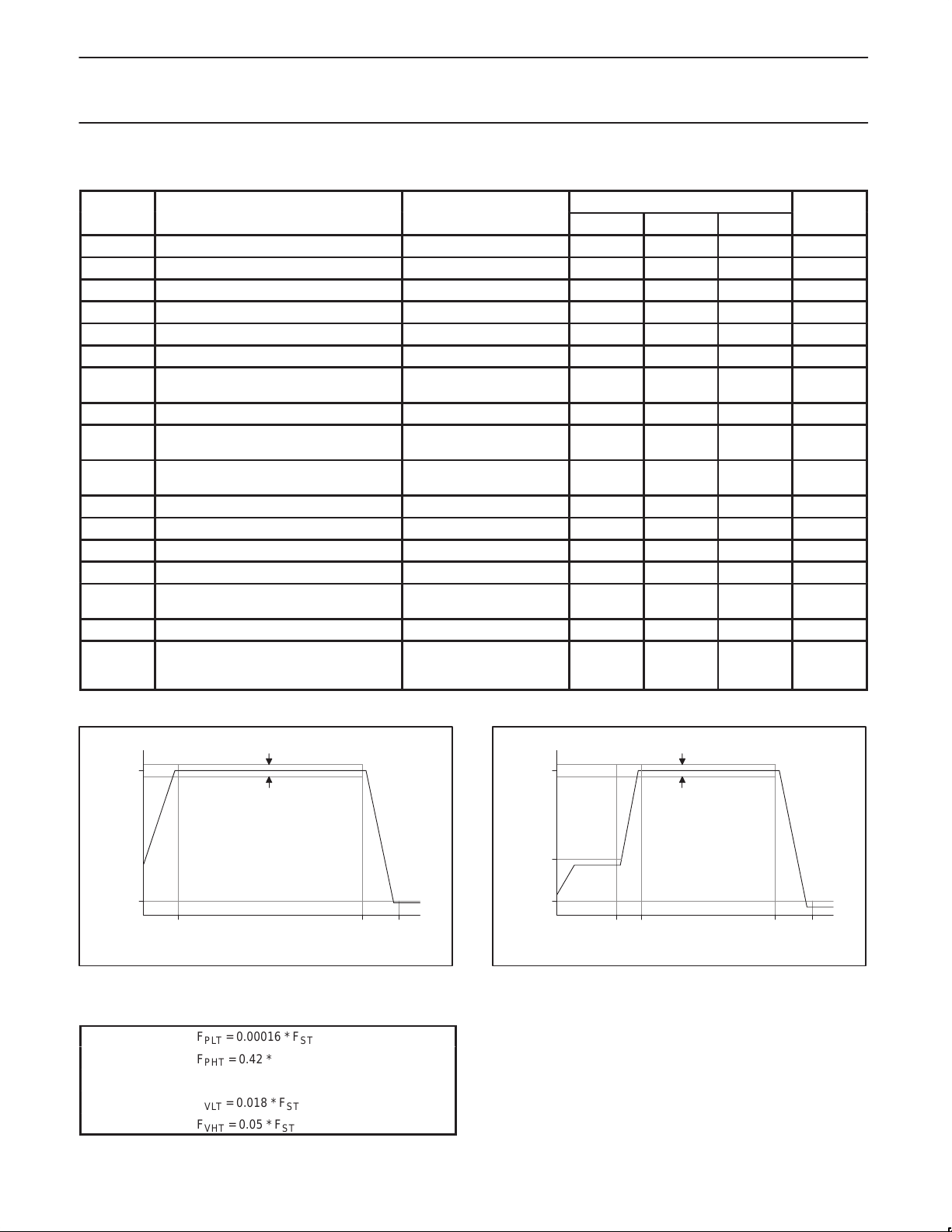
Figure 11. Telecom Input Frequency Response,
No Voice Filter
F
= 0.00016 * F
PLT
F
= 0.42 * F
PHT
F
= 0.6 * F
SHT
F
= 0.018 * F
VLT
F
= 0.05 * F
VHT
ST
ST
ST
ST
ST
PHT
F
SHT
SN00136
RIP
TI
0dB
SIB
VTI
SIB
HTI
F
VLT
F
VHT
FREQUENCY (Hz)
F
PHT
Figure 12. Telecom Input Frequency Response,
Voice Filter Enabled
F
SHT
SN00137
1998 May 08
14
Page 15
Philips Semiconductors Preliminary specification
SYMBOL
PARAMETER
CONDITIONS
UNIT
UCB1 100Advanced modem/audio analog front-end
6.2.2 Telecom Output Specifications
LIMITS
MIN TYP MAX
F
ST
V
OOT
V
TOUT
ROES
TO
SINAD
TO
RIP
TO
RIP
VTO
SBR
VTO
SBR
TO
E
ITO
Z
TELTO
V
OFFTO
NOTE: Coding scheme for the DAC input data is 2’s complement.
sample frequency 10 kHz
full scale output voltage differential Toutp/Toutn 4.0 4.4 V
DC bias voltage
Toutp / Toutn pins
telecom output path
enabled
1.4 V
resolution 14 bit
signal to noise + distortion 75 dB
pass band ripple 0.6 dB
pass band ripple,
voice band filter activated
stop band rejection,
voice filter activated
stop band rejection F
Fsig < F
VLT
< Fsig 70 dB
SHT
integrated out of band energy Frequencies > F
ST
25 mVrms
0.6 dB
minimal load impedance 600 Ω
offset error
(deviation of the analogue output from
zero with 0 code input to telecom out-
1200Ω load 50 mV
put path)
pp
RIP
TO
0dB
SBR
HTO
F
PLT
FREQUENCY (Hz)
F
PHT
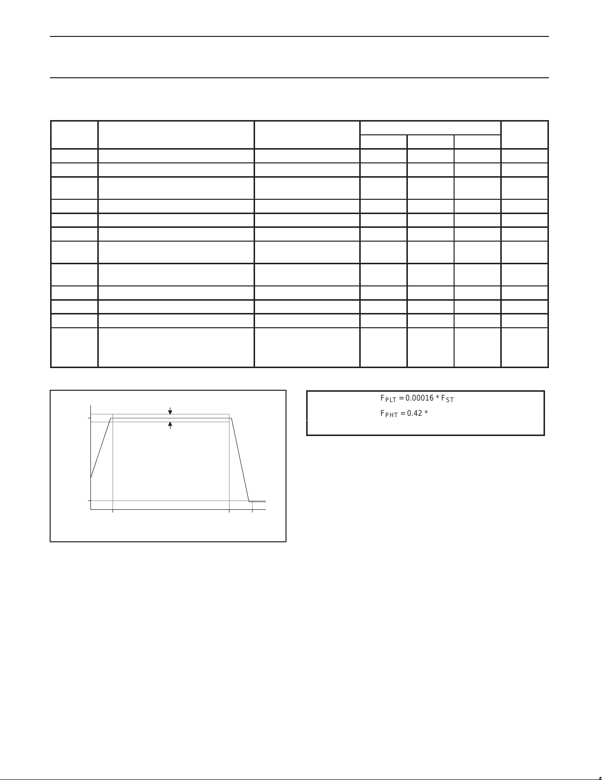
Figure 13. Telecom Output Frequency Response,
No Voice Filter
F
SHT
SN00138
F
= 0.00016 * F
PLT
F
= 0.42 * F
PHT
F
= 0.6 * F
SHT
ST
ST
ST
1998 May 08
15
Page 16
Philips Semiconductors Preliminary specification
UCB1 100Advanced modem/audio analog front-end
6.3 Touch Screen Measurement Modes
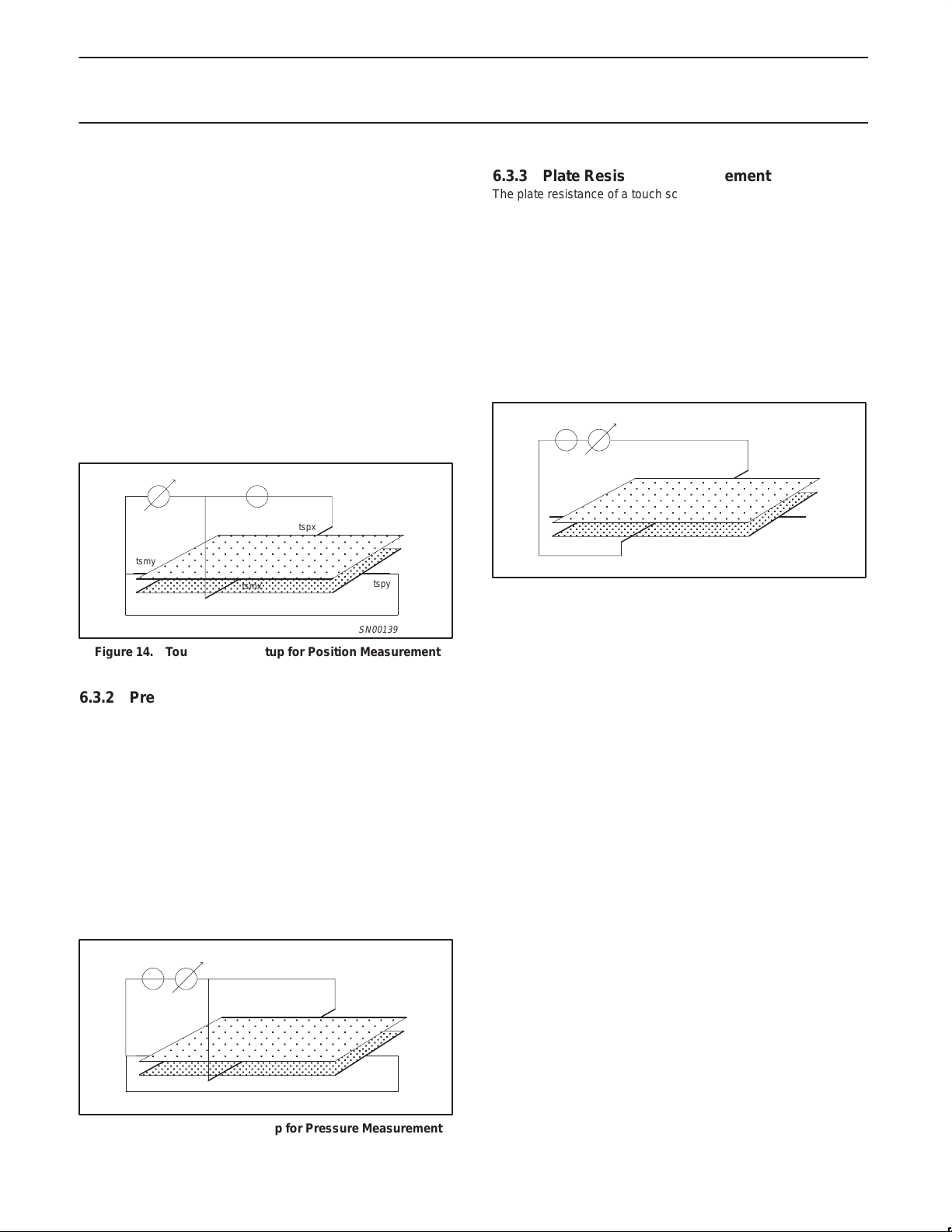
The UCB1100 contains an on chip interface for a 4 wire resistive
touch screen. This interface supports three modes of touch screen
measurements, position, pressure and plate resistance.
6.3.1 Position Measurement
Two position measurements are needed to determine the location of
the pressed spot. First an X measurement, secondly a Y
measurement. The X plate is biased during the X position
measurement the X plate and the voltage on one or both Y terminals
(tspy, tsmy) measured. The circuit can been represented by a
potentiometer , with the tspy and/or tsmy electrode being the ‘wiper’.
The measured voltage on the tspy/tsmy terminal is proportional to
the X position of the pressed spot of the touch screen.
In the Y position mode the X plate and Y plate terminals are
interchanged, thus the Y plate is biased on the voltage on the tspx
and/or tsmx terminal is measured.
VtscbiasVposition
tspx
tsmx
Xplate
tspy
SN00139
tsmy
Figure 14. Touch Screen Setup for Position Measurement
6.3.3 Plate Resistance Measurement
The plate resistance of a touch screen varies typically a lot due to
processing spreads. Knowing the actual plate resistance makes it
possible to compensate for the plate resistance effects in the
pressure resistance measurements. Secondly the plate resistance
decreases when two or more spots on the touch screen are
pressed. In that case a part of one plate, e.g. the X plate is shorted
by the other plate, which decreases the actual plate resistance.
The plate resistance measurement is executed in the same way as
the pressure resistance measurement. In this case only one of the
two plates is biased and the other plate is kept floating. The current
through the connected plate is again a direct indication of the
connected resistance.
Vtscbias iplate
tspx
tsmy
Figure 16. Touch Screen Setup for Plate Resistance
Xplate
tsmx
Measurement
tspy
SN00141
6.3.2 Pressure Measurement
The pressure used to press the touch screen can be determined. In
fact the contact resistance between the X and Y plate is measured,
which is a good indication of the size of the pressed spot and the
applied pressure. A soft stylus, e.g. a finger, leads to a rather large
contact area between the two plates when a large pressure is
applied. A hard stylus, e.g. a pen, leads to less variation in
measured contact resistance since the contact area is rather small.
One plate is biased at one or both terminals during this pressure
measurement, whereas the other plate is grounded, again on one or
both terminals. The current flowing through the touch screen is a
direct indication for the resistance between both plates. A
compensation for the series resistance, formed by the touch screen
plates itself will improve the accuracy of this measurement.
Vtscbiasipresure
tspx
Xplate
tsmy
tsmx
Figure 15. Touch Screen Setup for Pressure Measurement
tspy
SN00140
1998 May 08
16
Page 17
Philips Semiconductors Preliminary specification
UCB1 100Advanced modem/audio analog front-end
6.4 Touch Screen Interface
The UCB1100 contains a universal resistive touch screen interface
for 4 wire resistive touch screen, capable of performing both
position, pressure and plate resistance measurements. In addition
the touch screen can be programmed to generate interrupts when
the touch screen is pressed. The last mode is also active when the
UCB1100 is set in the standby mode.
tspx tspytsmx tsmy
ts.. power
ts.. ground
vssa3
adc_input_sel
analog mux
mux
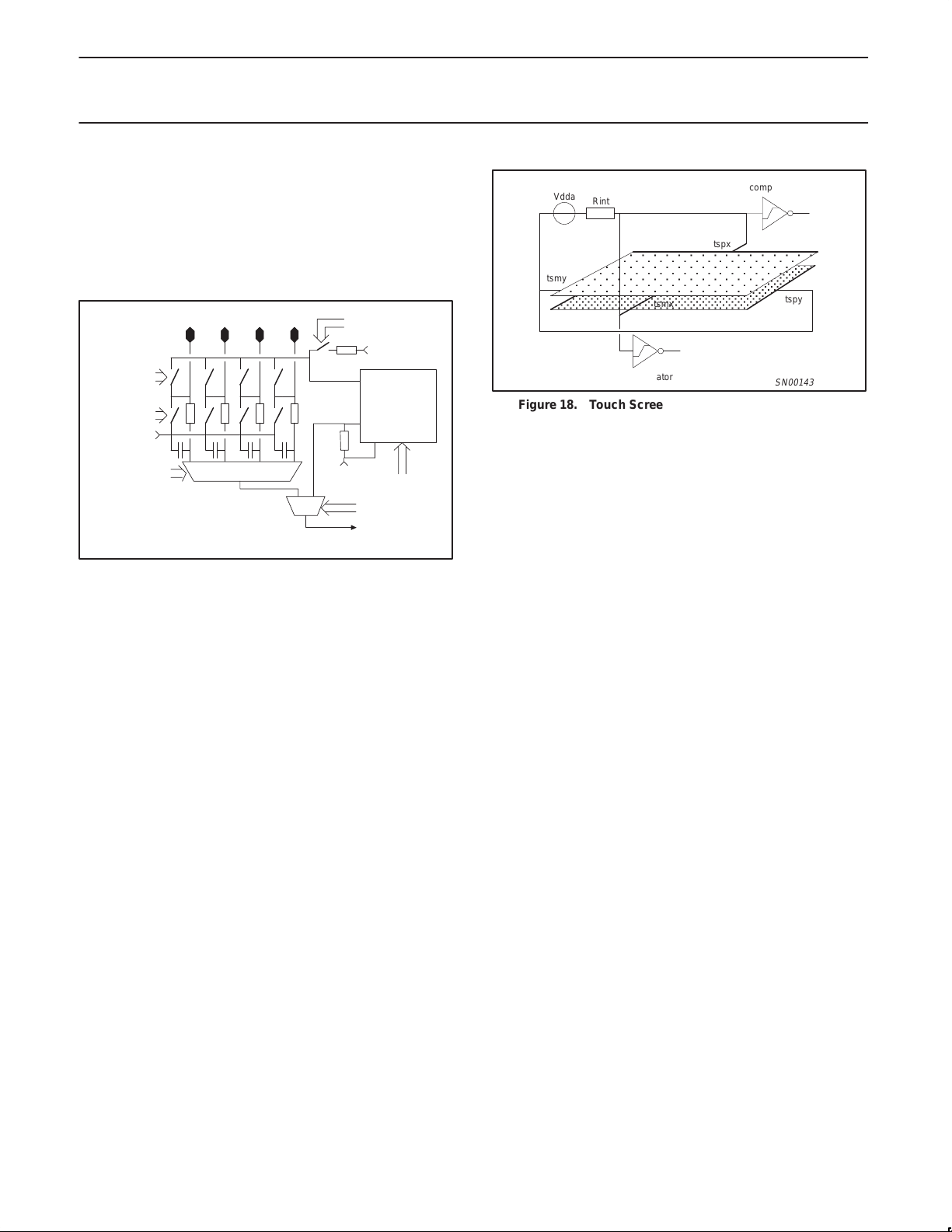
Figure 17. Block Diagram of the Touch Screen Interface
The touch screen interface connects to the touch screen by four
wires: tspx, tsmx, tspy and tsmy. Each of these pins can be
programmed to tbe floating, powered or grounded in the touch
screen switch matrix. The setting of each touch screen pin is
programmable by the
power ts..
and ground
screen control register. Possible conflicting settings (grounding and
powering of a touch screen pin at the same time) are detected by
the UCB1100. In that case the UCB1100 will ground the touch
screen pin.
The UCB1100’s internal voltage reference (Vref) is as reference
voltage for the touch screen bias circuitry. This makes the touch
screen biasing independent of supply voltage and temperature
variations. Four low pass filters, one on each touch screen terminal,
are built in to minimize the noise coupled from the LCD into the
touch screen signals. An LCD typically generates large noise
glitches on the touch screen, since they are closely coupled.
tsc_mod_sel
vdda1
touch screen
bias voltage
touch screen
current monitor
vssa1
tsc_bias_ena
tsc_mod_sel
to adc input
ts..
bits in the touch
SN00142
comparator
tspx
tspy
SN00143
tsmy
Vdda
Rint
Xplate
tsmx
comparator
Figure 18. Touch Screen Setup for Interrupt Detection
In addition to the measurements made above, the touch screen can
also act as an interrupt source. In this mode the X plate of the touch
screen has to be powered and the Y plate has to be grounded. In
this case the touch screen is not biased by the active touch screen
bias circuit, but by a resistor to vdda1. This configuration simply
biases the touch screen and the UCB1100 does not consume power
unless the touch screen is touched. The voltage on the X plate
terminals drops if the screen is pressed. This voltage drop is
detected by Schmitt trigger circuits, of which the outputs are
connected to the interrupt control block. An touch screen interrupt is
generated either when the touch screen is pressed (falling edge
enabled) or when the touch screen is released (rising edge
enabled). which can by used to activate the system around the
UCB1100 to start a touch screen readout sequence. The internal
Schmitt trigger circuits are connected to the tspx and tsmx signals
after the built in low pass filters. This reduces the number of
spurious interrupts, due to the coupling between the LCD screen
and the touch screen sensors.
Each of the four touch screen signals can be selected as input for
the built in 10 bit ADC, which is used to determine the voltage on the
selected touch screen pin. The flexible switch matrix and the multi
functional touch screen bias circuit enables the user of the UCB1100
to set each desired touch screen configuration.
The setting of the touch screen bias circuitry and the adc_input
multiplexer is determined by the setting of the
tsc_mod_sel
bits in
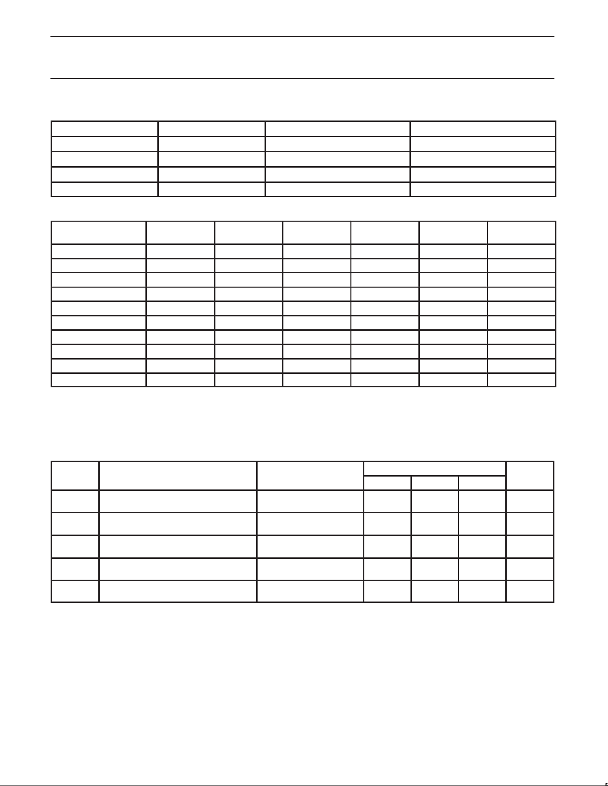
the touch screen control register according the following table.
1998 May 08
17
Page 18
Philips Semiconductors Preliminary specification
SYMBOL
PARAMETER
CONDITIONS
UNIT
UCB1 100Advanced modem/audio analog front-end
TOUCH SCREEN MODE SELECTION
tsc_mod_sel bits selected mode touch screen bias source ‘selected’ adc input
00 interrupt resistor to vdda1 defined by adc_input_sel bits
01 pressure touch screen bias circuit touch screen current monitor
10 position touch screen bias circuit defined by adc_inp_sel bits
11 position touch screen bias circuit defined by adc_input_sel bits
SUMMARY OF TOUCH SCREEN MODES
Touch screen mea-
surement
X position powered
Y position adc input
pressure – 1 powered
tspx tsmx tspy tsmy
1
2
1
grounded
adc input
powered
1
2
1
adc input
powered
grounded
2
1
1
adc input
grounded
grounded
2
1
1
pressure – 2 powered floating grounded floating pressure enabled
pressure – 3 floating grounded powered floating pressure enabled
pressure – 4 floating powered floating grounded pressure enabled
pressure – 5 grounded floating floating powered pressure enabled
X plate resistance powered
1
grounded
Y plate resistance floating floating powered
1
floating floating pressure enabled
1
grounded
1
interrupt powered powered grounded grounded interrupt disabled
NOTES:
1. The powered and grounded touch screen pins may be interchanged.
2. One of the two indicated touch screen pins have to be selected.
3. The touch screen bias has to be disabled in this mode by the user, to prevent false interrupts.
touch screen
mode
touch screen
bias
position enabled
position enabled
pressure enabled
pressure enabled
3
6.4.1 Touch Screen Specifications
V
TSCBIAS
I
TSCMAX
R
TSCINT
R
SWGND
t
TSCSTR
touch screen bias voltage
maximum touch screen current
maximum touch screen resistance to
generate an interrupt
on resistance ground switch
start up time touch screen bias voltage
generator
touch screen position mode
selected
touch screen position mode
selected
touch screen interrupt mode
selected
touch screen pin
programmed grounded
LIMITS
MIN TYP MAX
1.8 V
10 mA
2500 Ω
50 Ω
25 µs
1998 May 08
18
Page 19
Philips Semiconductors Preliminary specification
UCB1 100Advanced modem/audio analog front-end
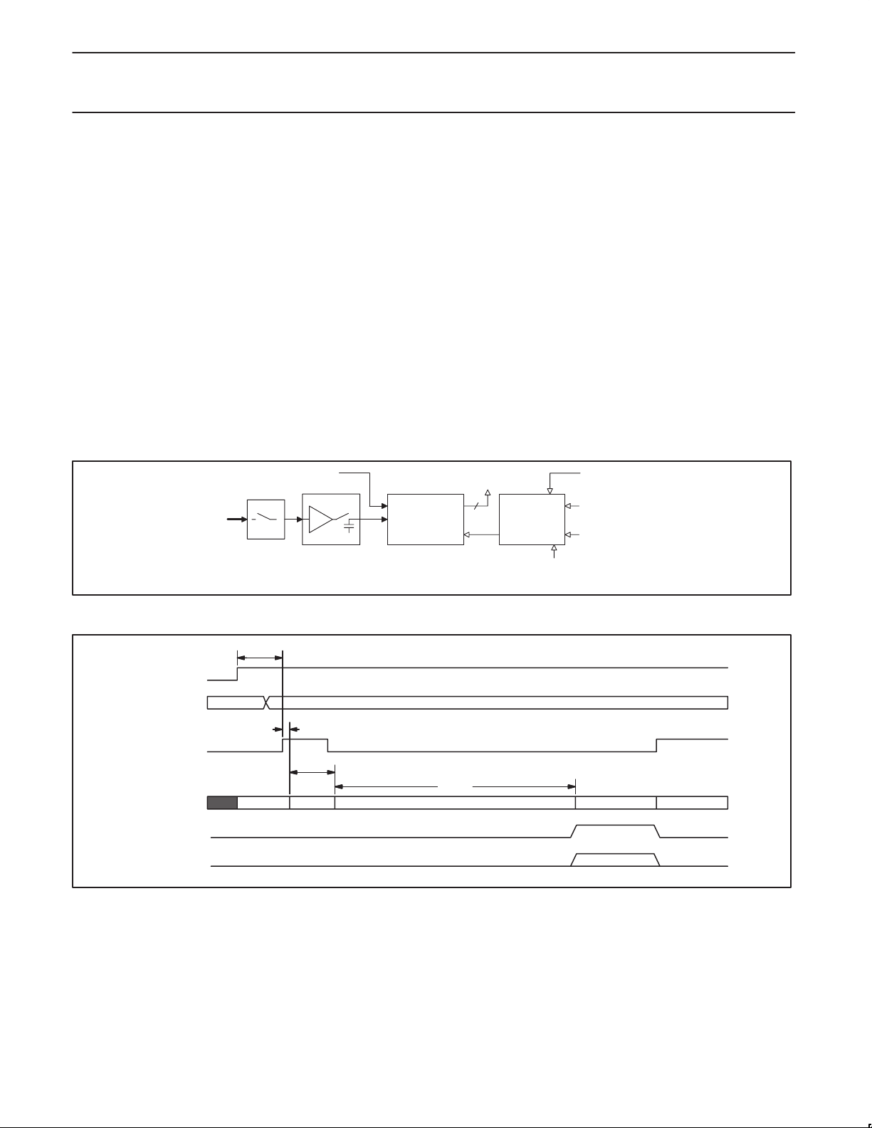
6.5 10 bit ADC
The UCB1100 includes a 10 bit successive approximation analogue
to digital converter (ADC) with build in track and hold circuitry, an
analogue multiplexer to select 4 analogue inputs or the 5 touch
screen voltages and 4 switched resistive voltage dividers on the
analogue ad0–3 high voltage inputs. The ADC is used to readout the
touch screen inputs and it measures the voltage on the four
analogue high voltage inputs ad0–3.
The ADC is controlled through the SIB interface. It is enabled by the
adc_enable
and hold circuitry does not consume any power when it is not
enabled.
A complete analogue to digital conversion consists of several
phases. First the ADC input selector must be set to the proper input.
Secondly the track and hold must track the signal; this requires a
certain settling time if the adc input was changed. After this time the
sample is taken. A calibration of the ADC circuitry is performed
before the actual conversion starts. The result of the conversion is
stored in the register 11 of the SIB interface, after the completion of
bit in register 10; the ADC circuitry, including the track
internal reference adcsync
mux
9 to 1
track & hold
Figure 19. Block Diagram of the 10 bit ADC Circuit
10 bit ADC
the conversion. An interrupt may be generated whenever a
conversion is completed, depending of the setting of the
adc_interrupt_ena
adc_data_valid
bits in the sib register 2 and 3. The
bit in the SIB register 11 indicates the status of the
ADC; it equals ‘0’ when a ADC sequence is started and it equals ‘1’
when the ADC result is stored in the SIB register 11.
The ADC sequence is started in two ways. First it starts whenever
the
adc_start
case when the
bit in register 10 is changed from ‘0’ to ‘1’; this is the
adc_sync_ena
bit in registers 10 equals ‘0’
(=default). Internal logic determines whether the adc input
multiplexer setting was changed in the sib frame, carrying the
adc_start bit transition. If this is the case, an additional tracking time
is added automatically.
The second mode of operation is activated when the adc_sync_ena
bit is set to ‘1’. In this mode the ADC conversion is not started by an
‘0’ to ‘1’ transition of the
adc_start
bis, but is ‘armed’. During the
arming situation the track and hold circuit tracks the selected input
signal. A sample is taken and the actual ADC conversion is started
when a rising edge is detected on the adcsync input pin.
to external register 11
10
ADC start
stop logic
adc_sync_ena
adc
start
sync
enable
SN00144
adc_ena
adc_input_selection
adc_start
’adc state’
adc_dat_valid
adc_data
tadcena
tadctrk
tadccal
tconv
track cal conversion track
SN00145
Figure 20. Timing Diagram of an ADC Conversion Sequence (adc_sync_ena=‘0’)
1998 May 08
19
Page 20
Philips Semiconductors Preliminary specification
UCB1 100Advanced modem/audio analog front-end
The ADC sequence is started in two ways. First it starts whenever
the
adc_start
case when the
bit in register 10 is changed from ‘0’ to ‘1’; this is the
adc_sync_ena
bit in registers 10 equals ‘0’
(=default). Internal logic determines whether the adc input
multiplexer setting was changed in the sib frame, carrying the
adc_start bit transition. If this is the case, an additional tracking time
is added automatically.
The second mode of operation is activated when the adc_sync_ena
bit is set to ‘1’. In this mode the ADC conversion is not started by an
‘0’ to ‘1’ transition of the
adc_start
bis, but is ‘armed’. During the
arming situation the track and hold circuit tracks the selected input
signal. A sample is taken and the actual ADC conversion is started
when a rising edge is detected on the adcsync input pin.
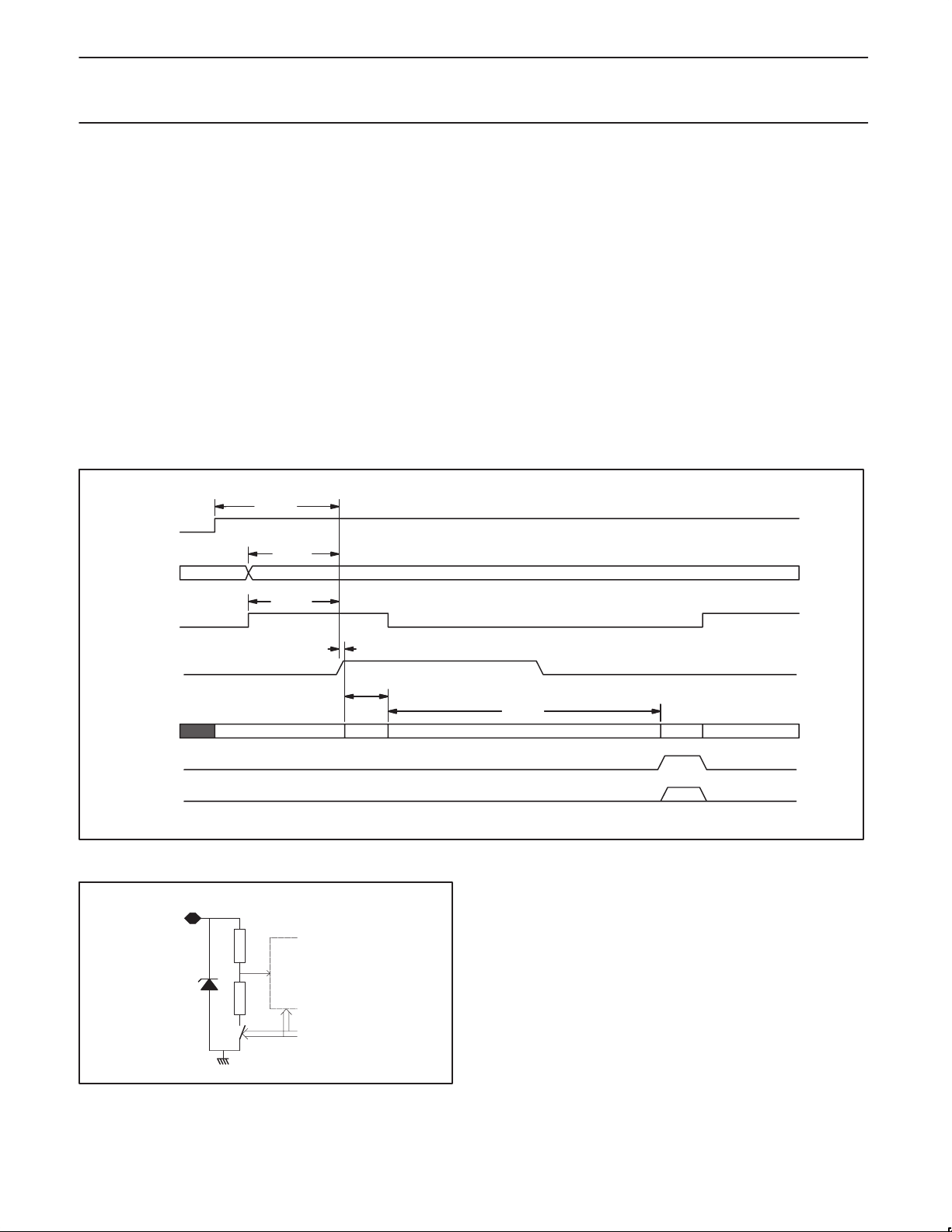
The internal ADC start logic adds a fixed tracking time, when the
ADC input multiplexer was changed in the SIB frame with the ‘0’ to
‘1’ transition of the adc_start bit. A rising edge on the adcsync pin
will not have any effect during this tracking time; the ADC sequence
tadcena
adc_ena
tadctrk
adc_input_selection
tadcdead
adc_start
will start on the first detected rising edge on the adcsyn pin after this
tracking time.
This mode is particulary useful when the internal ADC has to be
synchronized with the external systems. Typically it is used to
synchronize the readout of the touch screen with the driving of the
LCD screen, which is normally placed in the direct neighborhood of
the touch screen. Many spikes and a lot of ‘noise’ are superposed
on the touch screen signals, due to the close coupling of the touch
screen and the LCD.
The UCB1100 contains four high voltage analogue inputs ad0–3
which can be selected by the ADC input multiplexer, besides the
already discussed touch screen interface signals. These high
voltage inputs optimized to handle voltages larger than the applied
supply voltage. The built in resistive voltage divider are only
activated if the corresponding analogue input is selected. The not
selected ad0–3 inputs are high ohmic resulting in minimal leakage
input leakage of these pins.
adcsync
’adc state’
adc_dat_valid
adc_data
track cal conversion
Figure 21. Timing Diagram of an ADC Conversion Sequence (adc_sync_ena=‘1’)
ad0 or ad1 or ad2 or ad3
adc
input
switch
Figure 22. ad0–ad3 Resistive dividers
tadcstrs
tadccal
tconv
SN00146
adc_inp_sel[2:0]
SN00147
1998 May 08
20
Page 21
Philips Semiconductors Preliminary specification
SYMBOL
PARAMETER
CONDITIONS
UNIT
SYMBOL
PARAMETER
CONDITIONS
UNIT
UCB1 100Advanced modem/audio analog front-end
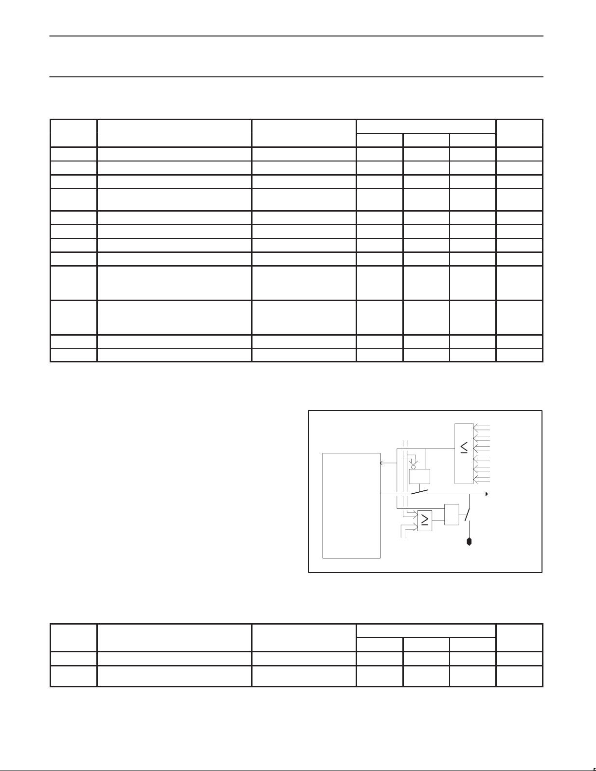
6.5.1 Specification Overview
LIMITS
MIN TYP MAX
RES
V
FSad
R
INad
I
Lad
DNL
ADC
INL
ADC
t
conv
t
adccal
t
adctrk
t
adctrks
t
hadcsync
t
padcsync
ADC
resolution of ADC 10 bit
full scale ad0–3 inputs 7.17 7.5 7.9 V
input impedance selected ad0–3 pin 50 75 100 Ω
input leakage current,
non selected ad0–3 pins
<1 10 µA
differential non-linearity 0.1 0.5 lsb
integral non linearity 0.5 2 lsb
conversion time 110 t
settling time 10 t
sibclk
sibclk
tracking time adc_sync_ena=‘0’
no adc input change 1 t
adc input change 50 t
sibclk
sibclk
tracking time adc_sync_ena=‘1’
no adc input change 25 ns
adc input change 50 t
sibclk
10 ns
6.6 On Chip Reference Circuit
The UCB1100 contains an on chip reference voltage source, which
generates the reference voltages for the 10 bit ADC and the
necessary internal reference voltages. Alternatively, the UCB1100
can be driven from an external reference voltage source.
The internal reference voltage can be monitored and filtered
additionally on the vrefbyp pin. Two bits in the ADC control register
determine the mode of operation of this reference voltage circuit.
The
vrefbyp_con
vrefbyp pin, while the
bit connects the internal reference voltage to the
ext_vref_ena
bit disables the internal
reference voltage and switches the UCB1100 into the external
voltage reference mode.
The internal reference circuit is activated only when one or more
analogue functions inside the UCB1100 is activated. This reduces
the current consumption of the analogue part in standby mode. The
external reference voltage source is also disconnected when all
analogue functions are disabled.
6.6.1 Specification Overview
V
REF
t
refstrt
reference voltage 1.1 1.2 1.3 V
start up time of internal reference voltage
circuit
aud_in_ena
aud_out_ena
tel_in_ena
tel_out_ena
tsc_bias_ena
adc_ena
internal
reference
voltage
SN00148
Internal
reference
circuitry
ext_vref_ena
vrefbyp_con
&
&
vrefbyp
Figure 23. Block Diagram of the Reference Circuit
LIMITS
MIN TYP MAX
50 t
sibclk
1998 May 08
21
Page 22
Philips Semiconductors Preliminary specification
UCB1 100Advanced modem/audio analog front-end
6.7 Serial Interface Bus
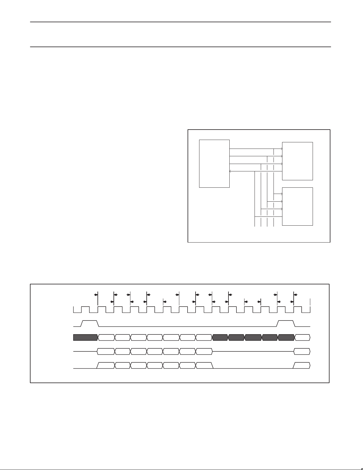
The UCB1100 serial interface bus (SIB) is compatible with industry
standard serial ports and devices, and is designed to connect
directly to a system controller. The sib protocol allows one or more
slave devices to be connected to the system controller. The data
transfer is always synchronous and it is frame based. The SIB
interface consists of four signals: sibddn, sibdout, sibclk and
sibsync.
Each SIB frame consists of at least 64 clock cycles. Typically 128
bits are used, divided into 2 sub frames of 64 bits each. The first
word (the bits 0 to 63) is read and/or written by the UCB1100, the
remaining bits may be used for communication between the system
controller and another slave device. The sibdout pin of the UCB1100
is default-stated for the bit 64 and higher in the SIB frame to prevent
bus conflicts with other slave devices. However when the
sib_zero_ena bit (control register 1) is set, the sibdout pin is forced
to zero for bit 64 and higher to prevent floating of the sibdout line
during this part of the sib frame in case when the UCB1100 is the
only slave device connected to the bus.
The UCB1100 always samples incoming data on the sibdin pin on
the falling edge of sibclk and it outputs data on the sibdout pin on
the rising edge of the sibclk. The start of a new sib frame is indicated
by a pulse on the sibsync line just before the start of this new sib
frame.
The applied clock signal to the sibclk pin is used as clock signal
inside the UCB1100; all internal clock signals are derived from that.
It is required that the sibclk signal is applied if one or more analogue
or digital functions is activated in the UCB1100; only the interrupt
controller is implemented synchronously. The sibclk may be stopped
when all digital and analogue functions are disabled; in that case the
lowest possible power consumption is meet. The sibclk should not
be stopped during a sib frame, but only at the end of the sib-frame,
to ensure that all analogue and digital functions are stopped
properly.
NOTE: The interrupt controller is still active, due to its
asynchronous implementation. The UCB1100 can
therefore still generate interrupts to the system controller,
when the sibclk is stopped.
The generation of the audio and telecom sample clocks require that
the sibclk signal is symmetrical: a non symmetrical sibclk will lead to
non equidistant sample moments, when an odd frequency divisor is
set in either of the audio or telecom control registers.
SIB MASTER
sibclk
sibsync
sibdout
sibdin
TO OTHER SIB SLAVES
UCB11001
sibclk
sibsync
sibdin
sibdout
SIB SLAVE 2
sibclk
sibsync
sibdin
sibdout
SN00149
Figure 24. Typical Connection Between the UCB1100 and the
System Controller
1998 May 08
sibclk
sibsync
sibdin
sibdout #1
sibdout #2
bit 0
bit 1
bit 2
bit 3 bit 63
bit 62 bit 64
bit 65 bit 126 bit 0
Figure 25. Serial Data Transmission of the UCB1100,
sibdout #1 in case sib_zero bit = ‘0’, sibdout #2 in case sib_zero bit = ‘1’
22
bit 127
SN00150
Page 23
Philips Semiconductors Preliminary specification
UCB1 100Advanced modem/audio analog front-end
6.7.1 SIB Data Format
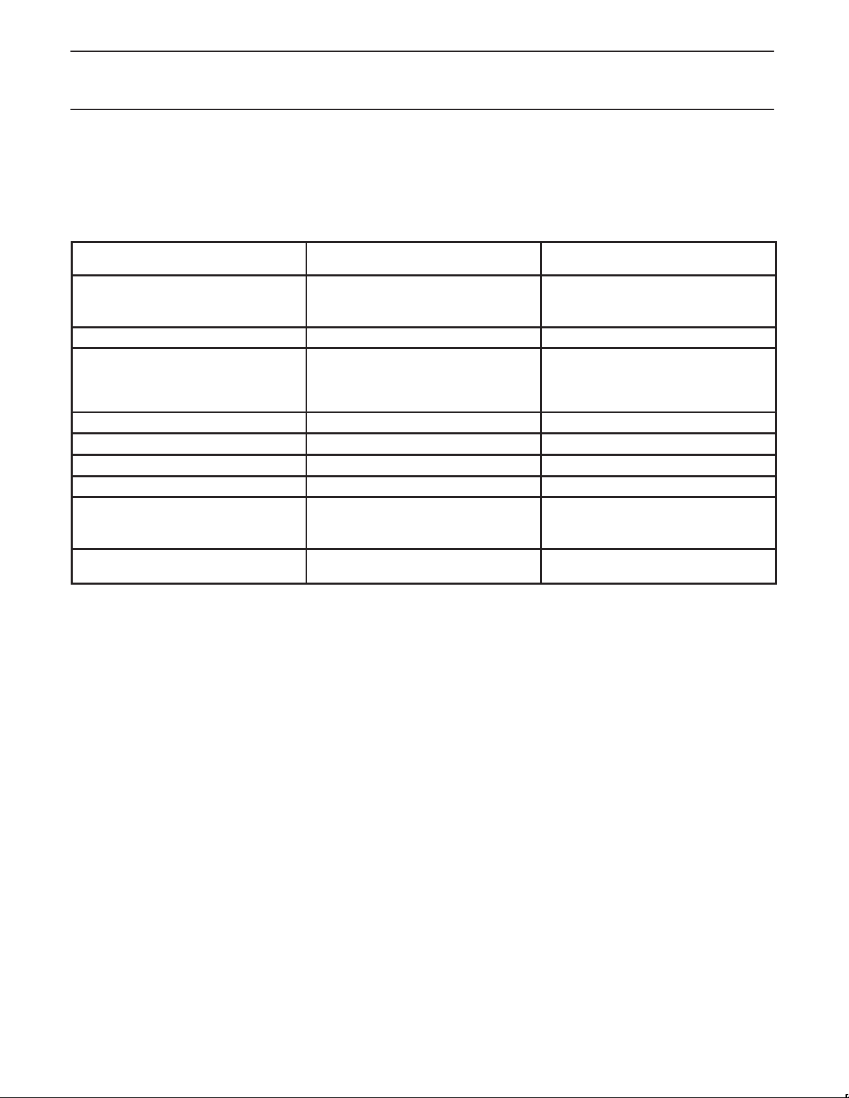
The first 64 bits in the sib-frame are read and written by the
UCB1100 and they contain both audio and telecom codec data
fields, several control bits and a control register data field as is
defined in table below.
Sib frame bit
15–0 audio input path data [15:0];
bit 0 = MSB,
the 12 MSB bits are read.
16 not read but reserved fixed ‘0’
20–17 control register address [3:0];
bit 0 = MSB
21 write bit (write = 1) fixed zero
29–22 not read but reserved fixed zeros
30 audio valid sample flag audio valid flag
31 telecom valid sample flag telecom valid flag
47–32 telecom input path data [15:0];
bit 0 = MSB,
the 14 MSB bits are read.
63–48 control register ‘write data [15:0];
bit 0 = MSB
NOTE:
Since the data transfer is completely synchronous, a given control register may be written many times, before the device feeding the data has a
chance to change the control bits. The UCB1100 does detect whether the data is changed or not.
SIBDin
field definition
audio output path data [15:0];
bit 0 = MSB,
the bits [15:12] are ‘0’
control register address [3:0];
bit 0 = MSB;
= copy of the register address as present in
the sibdin field in the same sib frame
telecom output path data [15:0],
bit 0 = MSB,
the bits [15:14] are ‘0’’
control register read data [15:0];
bit 0 = MSB
SIBDout
field definition
1998 May 08
23
Page 24
Philips Semiconductors Preliminary specification
UCB1 100Advanced modem/audio analog front-end
6.7.2 Codec Data Transfer
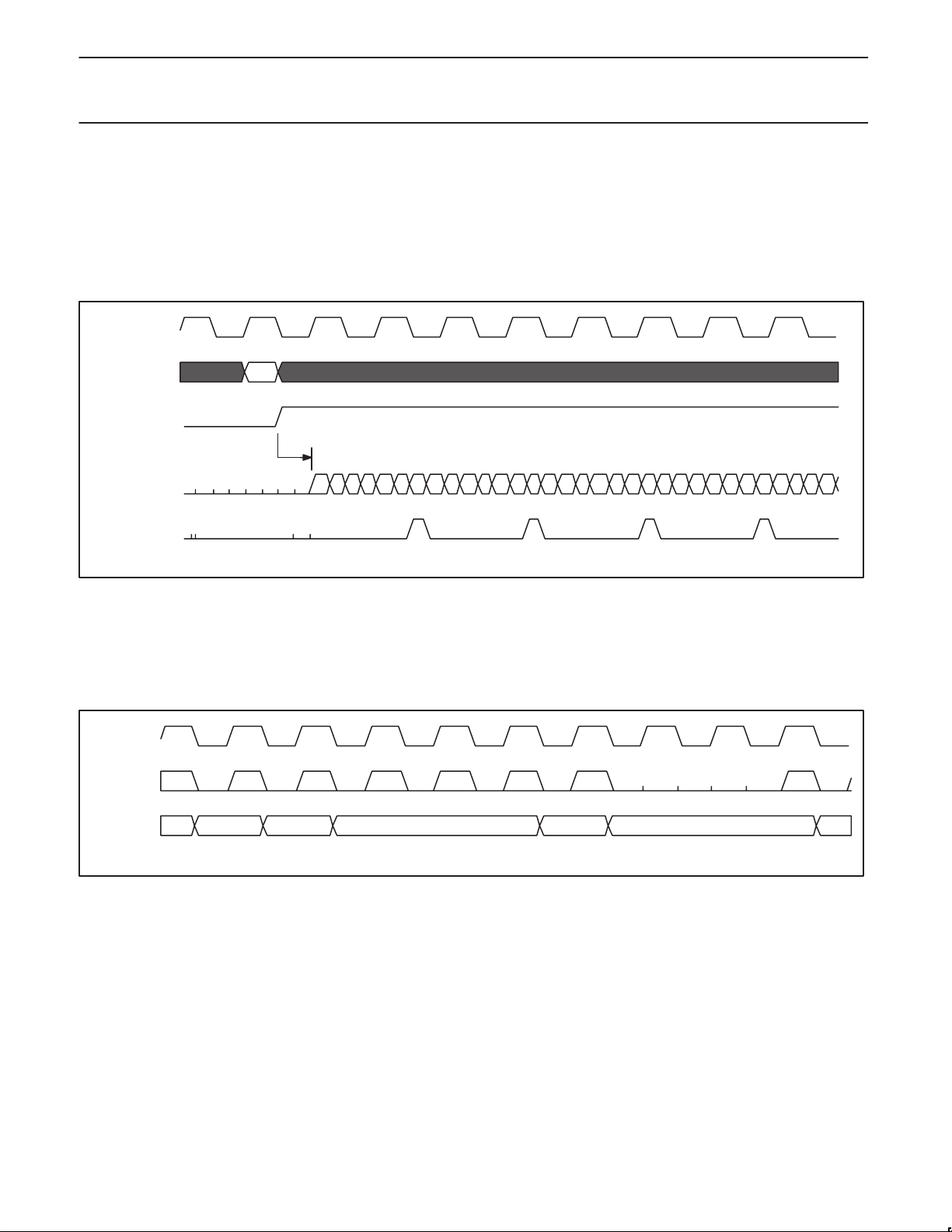
The audio and telecom codecs both operate at a programmable sample rate slower than the data transfer rate of the serial bus. The codecs
sample the contents of the appropriate field each time their internal counters indicate that a new sample is necessary. They update the data
read by the serial interface in the same manner. The counters for the audio and telecom subsystems are reset each time the respective
subsection is turned on (whenever the audio/telecom input or output path enable bits are set) and counting begins at the next SIBSync input
pulse (see Figure 26). The controlling devices must be both frequency and phase synchronized to the sample rate counters within the UCB1100
in order to ensure correct operation.
sibclk/128
sibdin
codec enable
sample counter
sample pulse
#1
tcodstr
01234560123456012345601234560123
SN00151
Figure 26. Start of the codec sample counters (divisor set to 7). Sibdin sub frame #1 contains the codec input and/or output path
enable bit, the codec enable signal is the ‘OR’ function of the associated code input and output enable bit.
The codec data is loaded in the codec input register after the sub frame has been sent completely, when the appropriate data valid flag was set
in the sib frame. The codec input data is not refreshed, whenever the audio and/or telecom data valid flag equals ‘0’ in the sub frame or when no
sibdin data is transmitted.
sibclk/128
sibdin stream
#1 #1 #1 #2 #2 #1 #1 #3 #3 #1
codec input data
N N+1 N+2 N+3 N+4 N+5
SN00152
Figure 27. Codec input data handshake protocol, sibdin frame #1 contains codec data and the data valid flag equals ‘1’,
sib frame #2 contains codec data, but the data valid flag equals ‘0’, sib frame #3 contains no data.
Codec data must be received by the UCB1100 in one of the SIB frames preceding the sample moment of the codec, it uses the last sample
received before the sample moment. In case no refreshed codec data has been sent, the UCB1100 re-uses the available ‘old’ codec data
sample. This will lead to high distortion in the codec circuits.
1998 May 08
24
Page 25
Philips Semiconductors Preliminary specification
UCB1 100Advanced modem/audio analog front-end
sibclk/128
sample
counter
sample pulse
60123456012345601234560123456012345
60123
sibdin
codec data
A,#1 B,#1 B,#2 C,#1 D,#1
sample B sample C
D,#1 D,#1 D,#1
sample D
sample D
E,#1 E,#2
sample E
SN00153
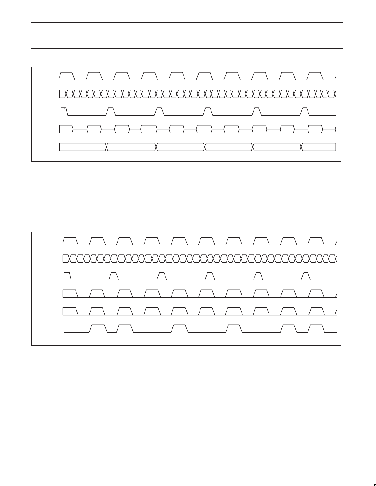
Figure 28. Codec input data transfer, sib frame x,#1 contains sample x data with the associate data valid flag set to ‘1’,
the sib frame indicated with x,#2 contain the codec sample x, with the associated data valid flag set to ‘0’.
The codec output data is transmitted in the first SIB frame following the sample moment of the codec. The sibdout data stream contains a data
valid bit for each codec (bit 30 and bit 31) to simplify the data transfer from the UCB1100 to the system controller. The audio and telecom data
valid bits are set to ‘1’ in the sibdout data stream when the codec generate reliable data. This is the case when the codec circuitry is stabilized
after it was enabled. This mode of operation is chosen when the
simplify the transfer of data, which is set when the
dyn_vflag_ena
dyn_vflag_ena
bit (register 13) equals ‘0’. A second mode is available to
bit is set to ‘1’. In that case the audio and the telecom data valid flag bits will
be ‘1’ in the sib frame following the codec sample moment, which contains at all times the most recent codec result.
sibclk/128
sample counter
sample pulse
audio data
01234560123456012345601234
6
N N N+1 N+2 N+2 N+3 N+3 N+4 N+4
56012345
60123
N+5
telecom data
data valid flag
N N+1 N+2 N+2 N+3 N+3 N+4
N+4 N+5
N+6
SN00154
Figure 29. Sample counter synchronization (divisor set to 7), audio and telecom data placement shown in sibdout data stream,
including the associated audio/telecom data valid flags (dynamic data valid flag mode).
The audio and telecom codec data each are positioned as if they had 16 bits of resolution. For the 12-bit audio codec the low 4 bits are ignored
on input and forced to 0 on output. For the 14-bit telecom codec, the low 2 bits are treated similarly.
1998 May 08
25
Page 26
Philips Semiconductors Preliminary specification
UCB1 100Advanced modem/audio analog front-end
6.7.3 Control Register Data Transfer
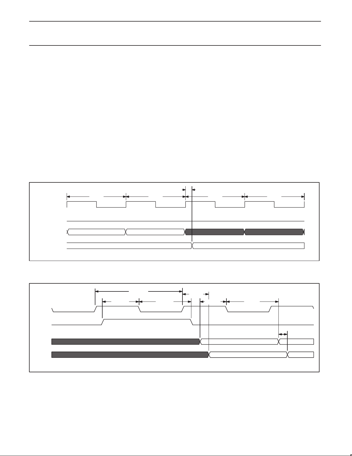
The last 16 bits of the UCB1100 word is made up of control register
data. The selection of the control register and whether it is read or
written is defined by the control register address field [bit 17:20] and
the “write” bit [bit 21]. For a read action on the a control register, the
control register address field has to set to the desired control
register address and the “write” bit has to be set to zero in the
SIBDin stream, The read data is sent by the UCB1100 within the
control register data field of SIBDout during the same frame as the
read request occurred. In addition, during a read cycle, the control
register data field of SIBDin is ignored by the UCB1100 which
implies that no modifications of the UCB1100 settings can be
performed when the “write” bit equals zero in the SIBDin
data-stream.
For a write cycle (“write” bit = 1), the control register data contents of
SIBDin are written to the UCB1100 register selected by the register
address field after receipt of the complete first word (the update is
performed during the 64th bit in the SIB frame). This implies that the
bit 64
sibclk
sibsync
control register data contents of SIBDout data-stream in a SIB frame
represents the previous contents of the selected control register.
The control register address in the sibdout data-stream is a copy of
the selected control register in the sibdin data-stream. These bits
show an additional delay since they pass additional circuitry in the
UCB1100.
The control register data is actually written in the control registers
after the transfer of the first sib word is completed. This implies that
the control register data is updated during bit 64 of the sib frame.
The control data is only updated when the write bit is ‘1’ in the sib
frame. The control data will not be updated when the write bit equals
‘0’. This simplifies the read out of control register data, since it is not
required to send ‘valid’ data in the control register data field when a
control register is read, if the write bit is kept at ‘0’.
The control register data in the sibdout stream is sampled just
before the sib frame is started. This implies that the returned control
register data represents the ‘old’ control data, in case new data was
provided in the sibdin data stream.
tpcdu
bit 65 bit 66bit 63
sibclk
sibsync
sibdin
sibdout
sibdin
control data
Figure 30. Control Register Update Timing
tsibclk
tsclsy thclsy tscldi thcldi
tpcldo
Figure 31. Timing Definitions SIB Interface
SN00155
tpdido
SN00156
1998 May 08
26
Page 27
Philips Semiconductors Preliminary specification
SYMBOL
PARAMETER
NOTES
UNIT
UCB1 100Advanced modem/audio analog front-end
6.7.4 AC Electrical Characteristics
T
= 0°C to 70°C, V
amb
V
= 3.3V ± 10%, V
DDD
1/t
sibclk
t
hsibclk/tsibclk
t
sclsy
t
hclsy
t
scldi
t
hcldi
t
pcldo
t
hcldo
t
pdido
t
pcdu
NOTES:
1. This is a requirement when an odd divisor is set either in the audio or in the telecom codec.
2. This is valid for all sib frame bits 0 to 63, except bits 17–20.
3. This is valid for the sib frame bits 17–20.
SSD
DDA1
= V
= V
SSA1
= 3.3V ± 10%, V
SSA2
= V
SSA3
= 3.3V ± 10%
DDA2
= 0V
LIMITS
MIN TYP MAX
sibclk input frequency 0 15 MHz
duty cycle sibclk Note 1 50 %
sibsync valid to falling edge sibclk ns
sibsync hold after falling edge sibclk ns
sibdin valid to falling edge sibclk ns
sibdin hold after falling edge sibclk ns
rising edge sibclk to valid sibdout Note 2 20 ns
sibdout hold after rising sibclk edge Note 3 ns
valid sibdin to valid sibdout 25 ns
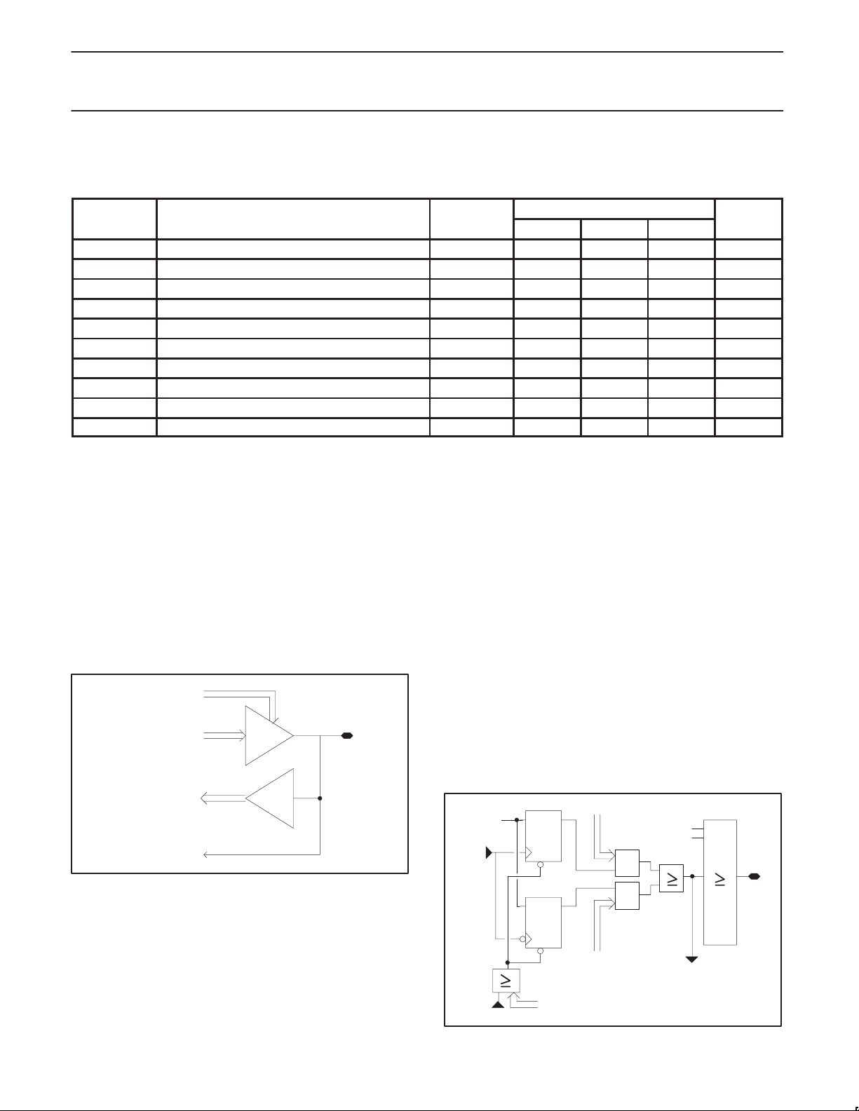
6.8 General Purpose IOs
The UCB1100 has 10 programmable digital input/output (IO) pins.
These pins can be independently programmed as input or output
using the IO_mode[0:9] bits in the control register 1. The output data
is determined by the content of the io_data bits in the control register
0, while the actual status of these pins can be read from the
io_data[0:9] bits in the control register 0.
The data on the io[0:9] pins are feed into the interrupt control block,
where they can generate an interrupt on the rising and/or falling
edge of these signals.
io_dir[x]
io_dat_in[x]
io_dat_out[x]
to interrupt module
Figure 32. Block Diagram of I/O Pin Circuitry
io[x]
SN00157
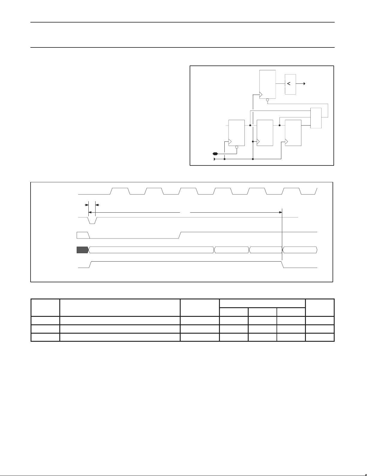
6.9 Interrupt Generation
The UCB1100 contains a programmable interrupt control block,
which can generate an interrupt for a ‘0’ to ‘1’ and/or a ‘1’ to ‘0’
transition on one or more of the IO[0:9] pins, the audio and telecom
clip detect, the adc_ready signal and the tspx_low and tsmx_low
signals.
The interrupt generation mode is set by the
register 2 and the
int_fal_ena
bits in the control register 3. The
actual interrupt status of each signal can be read from the control
register 4. The interrupt status is clear whenever a ‘1’ to ‘0’ transition
is written in control register 4 for the corresponding bit. The irqout
pin presents the ‘OR’ function of all interrupt status bits and can be
used to give an interrupt to the system controller.
The interrupt controller is implemented asynchronously. This provide
the possibly to generate interrupts when the sibclk is stopped,
e.g., an interrupt can be generated in power down mode, when the
touch screen is pressed or when the state of one of the io pins
changes.
ris_int_ena[x]
R
int.
source
‘1’
D
D
&
&
int_ris_ena
‘OR’ tree
bits in
irqout
1998 May 08
27
R
reset
fal_int_ena[x]
int_clear[x]
int_stat[x]
register 4 (read)
SN00158
Figure 33. Block Diagram of the Interrupt Controller
Page 28
Philips Semiconductors Preliminary specification
SYMBOL
PARAMETER
CONDITIONS
UNIT
UCB1 100Advanced modem/audio analog front-end
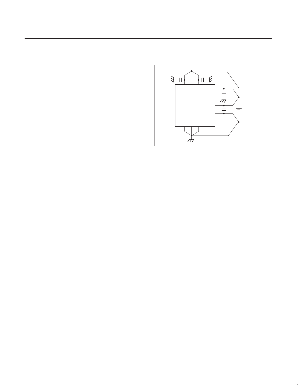
6.10 Reset Circuitry
The nreset signal is captured in the UCB1100 using a asynchronous
pulse stretching circuit. The nreset signal may be pulled down when
the sibclk is still stopped. The internal circuitry remembers this reset
signal and generates an internal reset signal from at least 5 sibclk
periods.
’1’
NRESET
sibclk
QQQ
D
R
Figure 34. Block Diagram of the Reset Circuitry
COUNT
D D
3
arstn
internal
reset
SN00159
&
t
lnrst
t
t
pclrsti
rsti
sibclk
tlnrst
trsti
nreset
arstn
count
internal reset
0123
Figure 35. Timing Diagram of the Reset Circuitry
LIMITS
MIN TYP MAX
nreset pulse width 5 ns
width of internal reset signal 5 * t
sibclk
delay between rising edge sibclk and internal reset 25 ns
SN00160
ns
1998 May 08
28
Page 29
Philips Semiconductors Preliminary specification
UCB1 100Advanced modem/audio analog front-end
7.0 MISCELLANEOUS
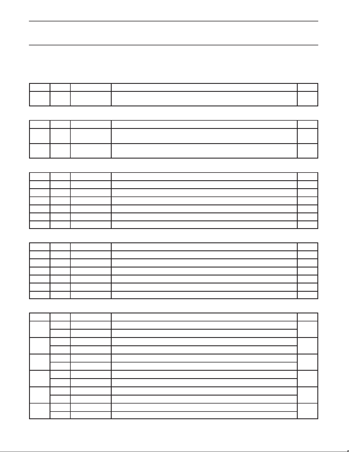
7.1 Power Routing Strategy
The UCB1100 has nine power supply pins, since the UCB1100
contains five power supply regions within the circuit. The analogue
and digital parts have their separate power supplies to reduce the
interference between these parts. The speaker driver circuit is
powered separately (vdda2/vssa2) from the other analogue circuit
parts and the touch screen switch matrix has its own ground pin
(vssa3). This separation in the analogue part reduces the
interference between the speaker driver and the touch screen switch
matrix, which has relatively large and fluctuating current
consumption and the remaining parts of the analog.
The vssd pins and the vssa1 pin are connected within the UCB1100
circuit. It is recommended to connect the vssd pins and the vssa1
directly to a ground plane on the PCB. The split in power supply
connections should be maintained on the PCB to get optimal
separation. Figure 36 shows the recommended PCB power supply
strategy.
vddd
UCB1100
vssa1
Figure 36. Recommended Power Supply Connection Strategy
vssd
vddd
vssd
vdda1
vdda2
vssa2
vssa3
3.3V supply
SN00161
1998 May 08
29
Page 30
Philips Semiconductors Preliminary specification
UCB1 100Advanced modem/audio analog front-end
8.0 CONTROL REGISTER OVERVIEW
Address 0: IO port data register
BIT MODE SYMBOL REMARK RESET
9:0 R/W io_data[9:0] The bits in the write register provide the data of the io pin when programmed as output.
The bits in the read register return the actual state of the associated io pin.
Address 1: IO port direction register
BIT MODE SYMBOL REMARK RESET
9:0 R/W io_dir[9:0] If ‘1’, the associated io pin is defined as output.
If ‘0’, the associated io pin is defined as input
15 R/W sib_zero If ‘1’, the sibdout pin is forced ‘0’ during the second sib word.
If ‘0’, the sibdout pin tristated during the second sib word
Address 2: Rising edge interrupt enable register
BIT MODE SYMBOL REMARK RESET
9:0 R/W io_ris_int[9:0] If ‘1’, the rising edge interrupt of the associated io pin is enabled 0
11 R/W adc_ris_int If ‘1’, the rising edge interrupt of the adc_ready signal is enabled 0
12 R/W tspx_ris_int If ‘1’, the rising edge interrupt of the tspx signal is enabled 0
13 R/W tsmx_ris_int If ‘1’, the rising edge interrupt of the tsmx signal is enabled 0
14 R/W tclip_ris_int If ‘1’, the rising edge interrupt of the telecom clip is enabled 0
15 R/W aclip_ris_int If ‘1’, the rising edge interrupt of the audio clip is enabled 0
0
0
0
Address 3: Falling edge interrupt enable register
BIT MODE SYMBOL REMARK RESET
9:0 R/W io_fal_int[9:0] If ‘1’, the falling edge interrupt of the associated io pin is enabled 0
11 R/W adc_fal_int If ‘1’, the falling edge interrupt of the adc_ready signal is enabled 0
12 R/W tspx_fal_int If ‘1’, the falling edge interrupt of the tspx signal is enabled 0
13 R/W tsmx_fal_int If ‘1’, the falling edge interrupt of the tsmx signal is enabled 0
14 R/W tclip_fal_int If ‘1’, the falling edge interrupt of the telecom clip is enabled 0
15 R/W aclip_fal_int If ‘1’, the falling edge interrupt of the audio clip is enabled 0
Address 4: Interrupt clear/status register
BIT MODE SYMBOL REMARK RESET
9:0
11
12
13
14
15
W io_int_clr[0:9] A ‘0’ to ‘1’ transition clears the interrupt of the associate io pin
R io_int_stat[9:0] Returns the actual interrupt status of the associated io pin
W adc_int_clr A ‘0’ to ‘1’ transition clears the interrupt adc_ready signal
R adc_int_stat Returns the actual interrupt status of the adc_ready signal
W tspx_int_clr A ‘0’ to ‘1’ transition clears the interrupt of the tspx signal
R tspx_int_stat Returns the actual interrupt status of the tspx signal
W tsmx_int_clr A ‘0’ to ‘1’ transition clears the interrupt of the tsmx signal
R tsmx_int_stat Returns the actual interrupt status of the tsmx signal
W tclip_int_clr A ‘0’ to ‘1’ transition clears the interrupt of the telecom clip
R tclip_int_stat Returns the actual interrupt status of the telecom clip
W aclip_int_clr A ‘0’ to ‘1’ transition clears the interrupt of the audio clip
R aclip_int_stat Returns the actual interrupt status of the audio clip
0
0
0
0
0
0
1998 May 08
30
Page 31
Philips Semiconductors Preliminary specification
UCB1 100Advanced modem/audio analog front-end
Address 5: Telecom control register A
BIT MODE SYMBOL REMARK RESET
6:0 R/W tel_div[6:0] Telecom codec sample rate divisor.
7 R/W tel_loop_ena If ‘1’, the loopback mode of within the telecom codec is enabled. 0
Valid values are between [0010000] (=16) and [1111111] (=127)
Address 6: Telecom control register B
BIT MODE SYMBOL REMARK RESET
3 R/W high_pass_ena] If ‘1’, the voice band filter in the telecom input path is enabled 0
4
6 R/W tel_att If ‘1’, the telecom input attenuation (6dB) is enabled. 0
11 R/W side_sup_ena If ‘1’, the sidetone suppression circuit is activated 0
13 R/W tel_mute If ‘1’, the telecom output is muted 0
14 R/W tel_in_ena If ‘1’, the telecom input path is activated 0
15 R/W tel_out_ena If ‘1’, the telecom output path is activated 0
R tel_clip The bit returns the actual telecom clip detection status.
W tel_clip A ‘0’ to ‘1’ transition bit clears the telecom clip detection status 0
16
Address 7: Audio control register A
BIT MODE SYMBOL REMARK RESET
6:0 R/W aud_div[6:0] Audio codec sample rate divisor.
Valid values lie between [00000110] (=6) and [1111111] (=127).
11:7 R/W aud_gain[4:0] Audio input gain setting.
Values range from [00000] (no gain) to [11111] (46.5dB gain)
Address 8: Audio control register B
BIT MODE SYMBOL REMARK RESET
4:0 R/W aud_att[4:0] Audio output attenuation setting.
Values range from [00000] (no attenuation) to [11111] (69dB attenuation).
6 R/W aud_clip_ena If ‘1’, the audio clip detection circuitry is activated 0
8 R/W aud_loop If ‘1’, the loopback mode in the audio codec is activated. 0
13 R/W aud_mute If ‘1’, the audio output is muted 0
14 R/W aud_in_ena If ‘1’, the audio codec input path is activated. 0
15 R/W aud_out_ena If ‘1’, the audio codec output path is activated. 0
6
0
0
1998 May 08
31
Page 32
Philips Semiconductors Preliminary specification
UCB1 100Advanced modem/audio analog front-end
Address 9: Touch screen control register
BIT MODE SYMBOL REMARK RESET
0 R/W tspx_pow If ‘1’, the tspx pin is powered 0
1 R/W tsmx_pow If ‘1’, the tsmx pin is powered 0
2 R/W tspy_pow If ‘1’, the tspy pin is powered 0
3 R/W tsmy_pow If ‘1’, the tspy pin is powered 0
4 R/W tspx_gnd If ‘1’, the tspx pin is grounded 0
5 R/W tsmx_gnd If ‘1’, the tsmx pin is grounded 0
6 R/W tspy_gnd If ‘1’, the tspy pin is grounded 0
7 R/W tsmy_gnd If ‘1’, the tspy pin is grounded 0
[9:8] R/W tsc_mode[1:0] T ouch screen operation mode
00 : interrupt mode
01 : pressure measurement mode
1x : position measurement mode
11 R/W tsc_bias_ena If ‘1’, the touch screen bias circuitry is activated. 0
12 R/W tspx_state This bit returns the inverted state of the tspx pin,
‘0’ is high voltage (pen up), ‘1’ is low voltage (pen down)
13 R/W tsmx_state This bit returns the inverted state of the tsmx pin,
‘0’ is high voltage (pen up), ‘1’ is low voltage (pen down)
0
Address 10: ADC control register
BIT MODE SYMBOL REMARK RESET
0 R/W adc_sync_ena If ‘1’, the adc sync mode is activated 0
1 R/W vrefbyp_con If ‘1’, the internal reference voltage is connected to the vrefbyp pin. 0
4:2 R/W adc_input[2:0] ADC input selection bits:
000: tspx
001: tsmx
010: tspy
011: tsmy
100 ad0
101: ad1
110: ad2
111: ad3
5 R/W ext_ref_ena If ‘1’, an external reference voltage has to be applied to the vrefbyp pin 0
7 R/W adc_start A ‘0’ to ‘1’ transition starts the adc conversion sequence. 0
15 R/W adc_ena If ‘1’, the adc circuit is activated 0
Address 11: ADC data register
BIT MODE SYMBOL REMARK RESET
14:5 R adc_data[9:0] Returns the ADC result 0
15 R adc_dat_val Returns ‘0’ if an adc conversion is in progress.
Returns ‘1’ if the 0 adc conversion is completed and the adc data is stored in the
adc_data[9:0] register.
Address 12: ID register
BIT MODE SYMBOL REMARK RESET
5:0 R version[5:0] Returns 000011 for all the UCB1100 circuits meeting this specification.
11:6 R device[5:0] Returns 000000 for all the UCB1100 circuits meeting this specification.
15:12 R supplier[3:0] Returns 0001 for all the UCB1100 circuits meeting this specification.
0
0
1998 May 08
32
Page 33
Philips Semiconductors Preliminary specification
UCB1 100Advanced modem/audio analog front-end
Address 13: Mode register
BIT MODE SYMBOL REMARK RESET
0 R/W aud_test If ‘1’, the analogue audio test mode is activated (Note 1) 0
1 R/W tel_test If ‘1’, the analogue telecom test mode is activated (Note 1) 0
5–2 R/W prod_test_mode These bits select the build in production test modes (Note 1) 0
12 R/W dyn_vflag_ena If ‘1’, the dynamic data valid flag mode is activated for both the audio and the telecom
data valid flag.
13 R/W aud_off_can If ‘1’, the offset cancelling circuit in the audio input path is disabled. 0
14 R/W Reserved bit for special function
15 R/W Reserved bit for special function
NOTES:
1. These bits can only be written if the test pin is ‘1’.
2. The functionality of the UCB1100 is changed when one or more test modes are activated.
Address 14: Reserved
BIT MODE SYMBOL REMARK RESET
This register is reserved for future use.
0
Address 15: Null register
BIT MODE SYMBOL REMARK RESET
15:0 R Returns [1111111111111111] at all times
1998 May 08
33
Page 34
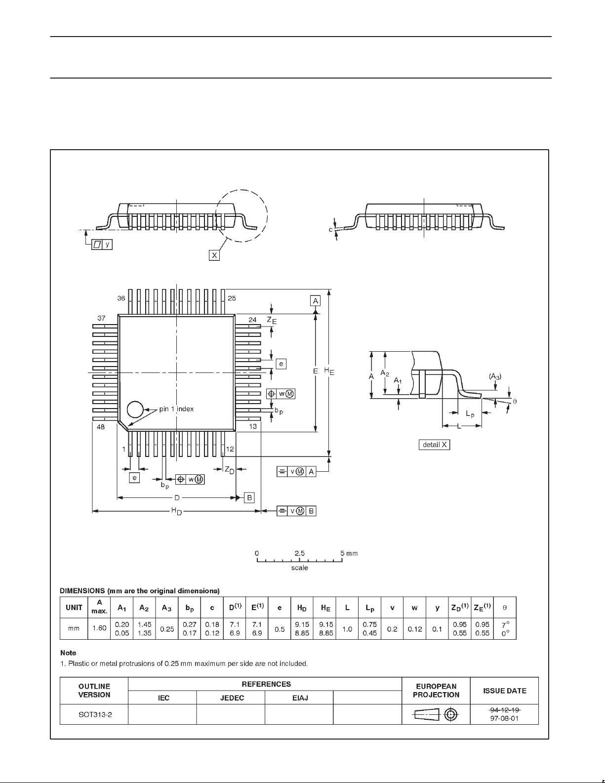
Philips Semiconductors Preliminary specification
UCB1 100Advanced modem/audio analog front-end
9.0 PACKAGE OUTLINES
9.1 LQFP48 LQFP48: plastic low profile quad flat package; 48 leads; body 7 x 7 x 1.4 mm SOT313-2
1998 May 08
34
Page 35

Philips Semiconductors Preliminary specification
UCB1 100Advanced modem/audio analog front-end
NOTES
1998 May 08
35
Page 36

Philips Semiconductors Preliminary specification
UCB1 100Advanced modem/audio analog front-end
10.0 DEFINITIONS
Data sheet status
Data sheet
status
Objective
specification
Preliminary
specification
Product
specification
Product
status
Development
Qualification
Production
Definition
This data sheet contains the design target or goal specifications for product development.
Specification may change in any manner without notice.
This data sheet contains preliminary data, and supplementary data will be published at a later date.
Philips Semiconductors reserves the right to make chages at any time without notice in order to
improve design and supply the best possible product.
This data sheet contains final specifications. Philips Semiconductors reserves the right to make
changes at any time without notice in order to improve design and supply the best possible product.
[1]
[1] Please consult the most recently issued datasheet before initiating or completing a design.
Definitions
Short-form specification — The data in a short-form specification is extracted from a full data sheet with the same type number and title. For
detailed information see the relevant data sheet or data handbook.
Limiting values definition — Limiting values given are in accordance with the Absolute Maximum Rating System (IEC 134). Stress above one
or more of the limiting values may cause permanent damage to the device. These are stress ratings only and operation of the device at these or
at any other conditions above those given in the Characteristics sections of the specification is not implied. Exposure to limiting values for extended
periods may affect device reliability.
Application information — Applications that are described herein for any of these products are for illustrative purposes only. Philips
Semiconductors make no representation or warranty that such applications will be suitable for the specified use without further testing or
modification.
Disclaimers
Life support — These products are not designed for use in life support appliances, devices or systems where malfunction of these products can
reasonably be expected to result in personal injury . Philips Semiconductors customers using or selling these products for use in such applications
do so at their own risk and agree to fully indemnify Philips Semiconductors for any damages resulting from such application.
Right to make changes — Philips Semiconductors reserves the right to make changes, without notice, in the products, including circuits, standard
cells, and/or software, described or contained herein in order to improve design and/or performance. Philips Semiconductors assumes no
responsibility or liability for the use of any of these products, conveys no license or title under any patent, copyright, or mask work right to these
products, and makes no representations or warranties that these products are free from patent, copyright, or mask work right infringement, unless
otherwise specified.
Philips Semiconductors
811 East Arques Avenue
P.O. Box 3409
Sunnyvale, California 94088–3409
Telephone 800-234-7381
Copyright Philips Electronics North America Corporation 1998
All rights reserved. Printed in U.S.A.
Date of release: 05-98
Document order number: 9397 750 03868
1998 May 08
36
 Loading...