

Page 1

+
–
16
3
4
ISENSE
5
2
PKLMT
14
13
12 1
9
VREF
VREF
VREF
RSETSSCT
15
VCC
VCC
11
7
VSENSE
8
6
10
VREF
VCC
ENA
IAC
VRMS
EMI
Filter
Line
Input
UC3854
VOUT
400 VDC
MULTOUT CAOUT
GTDRV
VAOUT
GND
Copyright © 2016, Texas Instruments Incorporated
Product
Folder
Order
Now
Technical
Documents
Tools &
Software
Support &
Community
SLUS336A –JUNE 1998–REVISED DECEMBER 2016
UCx854 High-Power Factor Preregulator
UC1854,UC2854,UC3854
1 Features
1
• Control Boost PWM to 0.99 Power Factor
• Limit Line-Current Distortion to < 5%
• World-Wide Operation Without Switches
• Feedforward Line Regulation
• Average Current-Mode Control
• Low Noise Sensitivity
• Low Startup Supply Current
• Fixed-Frequency PWM Drive
• Low-Offset Analog Multiplier and Divider
• 1-A Totem-Pole Gate Driver
• Precision Voltage Reference
2 Applications
• Offline AC-to-DC Converters
• Medical, Industrial, Telecom, and IT Power
Supplies
• Uninterruptible Power Supplies (UPS)
• Appliances and White Goods
3 Description
The UC1854 provides active-power factor correction
for power systems that otherwise would draw nonsinusoidal current from sinusoidal power lines. This
device implements all the control functions necessary
to build a power supply capable of optimally using
available power-line current while minimizing linecurrent distortion. To do this, the UC1854 contains a
voltage amplifier, an analog multiplier and divider, a
current amplifier, and a fixed-frequency PWM.
In addition, the UC1854 contains a power MOSFETcompatible gate driver, 7.5-V reference, line
anticipator, load-enable comparator, low-supply
detector, and overcurrent comparator.
The UC1854 uses average current-mode control to
accomplish fixed-frequency current control with
stability and low distortion. Unlike peak current-mode,
average current control accurately maintains
sinusoidal line current without slope compensation
and with minimal response to noise transients.
The high reference voltage and high oscillator
amplitude of the UC1854 minimize noise sensitivity
while fast PWM elements permit chopping
frequencies above 200 kHz. The UC1854 is used in
single-phase and three-phase systems with line
voltages that vary from 75 V to 275 V and line
frequencies across the 50-Hz to 400-Hz range. To
reduce the burden on the circuitry that supplies power
to this device, the UC1854 features low starting
supply current.
These devices are available packaged in 16-pin
plastic and ceramic dual in-line packages, and a
variety of surface-mount packages.
Device Information
PART NUMBER PACKAGE BODY SIZE (NOM)
SOIC (16) 7.50 mm × 10.30 mm
UC1854, UC2854,
UC3854
(1) For all available packages, see the orderable addendum at
the end of the data sheet.
PLCC (20) 8.96 mm × 8.96 mm
CDIP (16) 6.92 mm × 19.56 mm
PDIP (16) 6.35 mm × 19.30 mm
(1)
1
An IMPORTANT NOTICE at the end of this data sheet addresses availability, warranty, changes, use in safety-critical applications,
intellectual property matters and other important disclaimers. PRODUCTION DATA.
Block Diagram
Page 2

UC1854,UC2854,UC3854
SLUS336A –JUNE 1998–REVISED DECEMBER 2016
www.ti.com
Table of Contents
1 Features.................................................................. 1
2 Applications ........................................................... 1
3 Description ............................................................. 1
4 Revision History..................................................... 2
5 Device Comparison Table..................................... 3
6 Pin Configuration and Functions......................... 3
7 Specifications......................................................... 5
7.1 Absolute Maximum Ratings ...................................... 5
7.2 ESD Ratings.............................................................. 5
7.3 Recommended Operating Conditions....................... 6
7.4 Thermal Information.................................................. 6
7.5 Electrical Characteristics........................................... 6
7.6 Typical Characteristics.............................................. 8
8 Detailed Description............................................ 10
8.1 Overview ................................................................. 10
8.2 Functional Block Diagram....................................... 10
8.3 Feature Description................................................. 11
8.4 Device Functional Modes........................................ 11
9 Application and Implementation ........................ 12
9.1 Application Information............................................ 12
9.2 Typical Application.................................................. 12
10 Power Supply Recommendations ..................... 16
11 Layout................................................................... 16
11.1 Layout Guidelines ................................................. 16
11.2 Layout Example .................................................... 17
12 Device and Documentation Support ................. 18
12.1 Documentation Support ........................................ 18
12.2 Related Links ........................................................ 18
12.3 Receiving Notification of Documentation Updates 18
12.4 Community Resources.......................................... 18
12.5 Trademarks........................................................... 18
12.6 Electrostatic Discharge Caution............................ 18
12.7 Glossary................................................................ 18
13 Mechanical, Packaging, and Orderable
Information........................................................... 18
4 Revision History
NOTE: Page numbers for previous revisions may differ from page numbers in the current version.
Changes from Original (June 1998) to Revision A Page
• Added Applications section, Device Information table, Pin Configuration and Functions section, Specifications
section, ESD Ratings table, Recommended Operating Conditions table, Detailed Description section, Application
and Implementation section, Power Supply Recommendations section, Layout section, Device and Documentation
Support section, and Mechanical, Packaging, and Orderable Information section................................................................ 1
• Added Thermal Information table ........................................................................................................................................... 6
• Changed IAC value in both Multiplier Output vs Multiplier Inputs images from mA to µA. ................................................... 8
2
Submit Documentation Feedback Copyright © 1998–2016, Texas Instruments Incorporated
Product Folder Links: UC1854 UC2854 UC3854
Page 3

4CAOUT
5ISENSE
6NC
7MULTOUT
8IAC
9VAOUT
10VRMS
11NC
12VREF
13ENA
14 VSENSE
15 RSET
16 NC
17 SS
18 CT
19 VCC
20 GTDRV
1 NC
2 GND
3 PKLMT
Not to scale
1GND 16 GTDRV
2PKLMT 15 VCC
3CAOUT 14 CT
4ISENSE 13 SS
5MULTOUT 12 RSET
6IAC 11 VSENSE
7VAOUT 10 ENA
8VRMS 9 VREF
Not to scale
UC1854,UC2854,UC3854
www.ti.com
SLUS336A –JUNE 1998–REVISED DECEMBER 2016
5 Device Comparison Table
PARAMETER UC3854 UC3854A UC3854B
Supply current, OFF 2-mA maximum 400-µA maximum 400-µA maximum
Supply voltage (VCC) 35-V maximum 22-V maximum 22-V maximum
VCC turn-on threshold 16-V typical 16-V typical 10.5-V typical
VCC UVLO hysteresis 6-V typical 6-V typical 0.5-V typical
Current amplifier bandwidth 1-MHz typical 5-MHz typical 5-MHz typical
Current amplifier offset 4-mV, –4-mV maximum 0-mV, –4-mV maximum 0-mV, –4-mV maximum
MULTOUT voltage (high) 2.5-V typical 5-V typical 5-V typical
Multiplier gain tolerance Not specified –0.9 to –1.1 –0.9 to –1.1
ENABLE propagation delay Not specified 300-ns typical 300-ns typical
VSENSE input 7.5 V 3 V 3 V
IAC voltage 6-V typical 0.5-V typical 0.5-V typical
Voltage amplifier clamp — Internal Internal
Current amplifier clamp — Internal Internal
VREF good circuitry — Internal Internal
6 Pin Configuration and Functions
DW, J, and N Packages
16-Pin SOIC, CDIP, and PDIP
Top View
Product Folder Links: UC1854 UC2854 UC3854
FN Package
20-Pin PLCC
Top View
Submit Documentation FeedbackCopyright © 1998–2016, Texas Instruments Incorporated
3
Page 4
SET T
1.25
R C=´
UC1854,UC2854,UC3854
SLUS336A –JUNE 1998–REVISED DECEMBER 2016
PIN
NAME
CAOUT 3 4 O
CT 14 18 I
ENA 10 13 I
GND 1 2 —
GTDRV 16 20 O
IAC 6 8 I
ISENSE 4 5 I
MULTOUT 5 7 I/O
NC —
PKLMT 2 3 I
RSET 12 15 I
SS 13 17 I
VAOUT 7 9 O
CDIP,
PDIP,
SOIC
PLCC
1, 6,
11, 16
I/O DESCRIPTION
Current amplifier output. This is the output of a wide-bandwidth operational amplifier that senses line
current and commands the pulse-width modulator (PWM) to force the correct current. This output
swings close to GND, allowing the PWM to force zero duty cycle when necessary. The current
amplifier remains active even if the IC is disabled. The current-amplifier output stage is an NPN
emitter-follower pullup and an 8-kΩ resistor to ground.
Oscillator timing capacitor. A capacitor from CT to GND sets the PWM oscillator frequency.
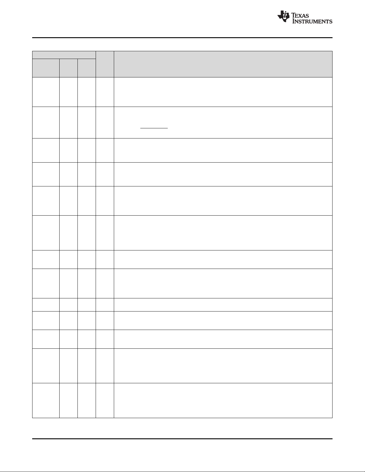
Use Equation 1:
Enable. ENA is a logic input that enables the PWM output, voltage reference, and oscillator. ENA
also releases the soft-start clamp, allowing SS to rise. When not in use, connect ENA to a 5-V supply
or pull ENA high with a 22-kΩ resistor. The ENA pin is not intended to be used as a high speed
shutdown to the PWM output.
Ground. All voltages are measured with respect to GND. VCC and VREF must be bypassed directly
to GND with an 0.1-µF or larger ceramic capacitor. The timing capacitor discharge current also
returns to this pin, so the lead from the oscillator timing capacitor to GND must also be as short and
as direct as possible.
Gate drive. The output of the PWM is a totem-pole MOSFET gate driver on GTDRV. This output is
internally clamped to 15 V so that the IC operates with VCCas high as 35 V. Use a series gate
resistor of at least 5 Ω to prevent interaction between the gate impedance and the GTDRV output
driver that might cause the GTDRV output to overshoot excessively. Some overshoot of the GTDRV
output is always expected when driving a capacitive load.
Input AC current. This input to the analog multiplier is a current. The multiplier is tailored for very low
distortion from this current input (IAC) to MULTOUT, this is the only multiplier input that must be used
for sensing instantaneous line voltage. The nominal voltage on IAC is 6 V, in addition to a resistor
from IAC to rectified 60 Hz, connect a resistor from IAC to REF. If the resistor to VREF is one-fourth
of the value of the resistor to the rectifier, then the 6-V offset is cancelled, and the line current has
minimal cross-over distortion.
Current-sense minus. This is the inverting input to the current amplifier. This input and the noninverting input, MULTOUT, remain functional down to and below GND. Take care to avoid taking
these inputs below –0.5 V because they are protected with diodes to GND.
Multiplier output and current-sense plus. The output of the analog multiplier and the non-inverting
input of the current amplifier are connected together at MULTOUT. The cautions about taking
ISENSE below –0.5 V also apply to MULTOUT. As the multiplier output is a current, this is a highimpedance input similar to ISENSE, so the current amplifier can be configured as a differential
amplifier to reject GND noise. Figure 9 shows an example of using the current amplifier differentially.
— No connection
Peak current limit. The threshold for PKLMT is 0 V. Connect this input to the negative voltage on the
current-sense resistor as shown in Figure 9. Use a resistor to VREF to offset the negative currentsense signal up to GND.
Oscillator charging current and multiplier limit set. A resistor from RSET to GND programs oscillator
charging current and maximum multiplier output. Multiplier output current does not exceed 3.75 V
divided by the resistor from RSET to GND.
Soft start. SS remains at GND as long as the device is disabled or VCCis too low. SS pulls up to
over 8 V by an internal 14-mA current source when both VCCbecomes valid and the IC is enabled.
SS acts as the reference input to the voltage amplifier if SS is below VREF. With a large capacitor
from SS to GND, the reference to the voltage regulating amplifier rises slowly, and increases the
PWM duty cycle slowly. In the event of a disable command or a supply dropout, SS quickly
discharges to ground and disables the PWM.
Voltage amplifier output. This is the output of the operational amplifier that regulates output voltage.
Like the current amplifier, the voltage amplifier remains active even if the IC is disabled with either
ENA or VCC. This means that large feedback capacitors across the amplifier stay charged through
momentary disable cycles. Voltage amplifier output levels below 1 V inhibit multiplier output. The
voltage amplifier output is internally limited to approximately 5.8 V to prevent overshoot. The voltage
amplifier output stage is an NPN emitter-follower pullup and an 8-kΩ resistor to ground.
www.ti.com
Pin Functions
(1)
4
Submit Documentation Feedback Copyright © 1998–2016, Texas Instruments Incorporated
Product Folder Links: UC1854 UC2854 UC3854
Page 5
www.ti.com
PIN
NAME
VCC 15 19 —
VREF 9 12 O
VRMS 8 10 I
VSENSE 11 14 I
CDIP,
PDIP,
SOIC
PLCC
7 Specifications
UC1854,UC2854,UC3854
SLUS336A –JUNE 1998–REVISED DECEMBER 2016
Pin Functions (continued)
I/O DESCRIPTION
Positive supply voltage. Connect VCC to a stable source of at least 20 mA above 17 V for normal
operation. Also bypass VCC directly to GND to absorb supply current spikes required to charge
external MOSFET gate capacitances. To prevent inadequate GTDRV signals, these devices are
inhibited unless VCCexceeds the upper undervoltage-lockout threshold and remains above the lower
threshold.
Voltage reference output. VREF is the output of an accurate 7.5-V voltage reference. This output is
capable of delivering 10 mA to peripheral circuitry and is internally short-circuit current limited. VREF
is disabled and remains at 0 V when VCCis low or when ENA is low. Bypass VREF to GND with an
0.1-µF or larger ceramic capacitor for best stability.
RMS line voltage. The output of a boost PWM is proportional to the input voltage, so when the line
voltage into a low-bandwidth boost PWM-voltage regulator changes, the output changes immediately
and slowly recovers to the regulated level. For these devices, the VRMS input compensates for line
voltage changes if it is connected to a voltage proportional to the RMS input line voltage. For best
control, the VRMS voltage must stay between 1.5 V and 3.5 V.
Voltage amplifier inverting input. This is normally connected to a feedback network and to the boost
converter output through a divider network.
7.1 Absolute Maximum Ratings
over operating free-air temperature range (unless otherwise noted)
Supply voltage VCC 35 V
VSENSE, VRMS 11
Input Voltage
PKLMT 5
Gate driver current Input current
Input current RSET, IAC, PKLMT, ENA 10 mA
Power dissipation 1 W
Storage temperature, T
(1) Stresses beyond those listed under Absolute Maximum Ratings may cause permanent damage to the device. These are stress ratings
only, which do not imply functional operation of the device at these or any other conditions beyond those indicated under Recommended
Operating Conditions. Exposure to absolute-maximum-rated conditions for extended periods may affect device reliability.
(2) All voltages with respect to GND.
(3) All currents are positive into the specified terminal.
(4) ENA input is internally clamped to approximately 14 V.
(5) Consult Unitrode Integrated Circuits databook for information regarding thermal specifications and limitations.
stg
50% duty cycle 1.5
Continuous 0.5
(1)(2)(3) (4)(5)
MIN MAX UNIT
VISENSE, MULTOUT 11
A
–65 150 °C
7.2 ESD Ratings
VALUE UNIT
V
(ESD)
(1) JEDEC document JEP155 states that 500-V HBM allows safe manufacturing with a standard ESD control process.
(2) JEDEC document JEP157 states that 250-V CDM allows safe manufacturing with a standard ESD control process.
Electrostatic discharge
Human-body model (HBM), per ANSI/ESDA/JEDEC JS-001
Charged-device model (CDM), per JEDEC specification JESD22-C101
(1)
(2)
±2500
±1500
V
Product Folder Links: UC1854 UC2854 UC3854
Submit Documentation FeedbackCopyright © 1998–2016, Texas Instruments Incorporated
5
Page 6

UC1854,UC2854,UC3854
SLUS336A –JUNE 1998–REVISED DECEMBER 2016
www.ti.com
7.3 Recommended Operating Conditions
over operating free-air temperature range (unless otherwise noted)
MIN MAX UNIT
V
CC
T
J
Supply voltage 10 20
UC1854 –55 125
Operating junction temperature
UC3854 0 70
7.4 Thermal Information
UCx854
THERMAL METRIC
R
θJA
R
θJC(top)
R
θJB
ψ
JT
ψ
JB
R
θJC(bot)
Junction-to-ambient thermal resistance 71.5 — 25 40.8 °C/W
Junction-to-case (top) thermal resistance 32.7 — — 26.8 °C/W
Junction-to-board thermal resistance 36.3 — 5.5 20.9 °C/W
Junction-to-top characterization parameter 6.8 — 2.1 10.9 °C/W
Junction-to-board characterization
parameter
Junction-to-case (bottom) thermal
resistance
(1) For more information about traditional and new thermal metrics, see the Semiconductor and IC Package Thermal Metricsapplication
report.
(1)
UNITDW (SOIC) FN (PLCC) J (CDIP) N (PDIP)
16 PINS 20 PINS 16 PINS 16 PINS
35.8 — 5.4 20.7 °C/W
— — 3.4 — °C/W
°CUC2854 –40 85
7.5 Electrical Characteristics
Unless otherwise stated, VCC= 18 V, R
V
= 1.5 V, IAC= 100 µA, V
RMS
ISENSE
VREF, GTDRV, TA= TJ, TA= –55°C to 125°C for the UC1854, TA= –40°C to 85°C for the UC2854,
and TA= 0°C to 70°C for the UC3854.
PARAMETER TEST CONDITIONS MIN TYP MAX UNIT
OVERALL
Supply current, OFF V
Supply current, ON 10 16 mA
VCCturn-on threshold 14.5 16 17.5 V
VCCturn-off threshold 9 10 11 V
ENA threshold, rising 2.4 2.55 2.7 V
ENA threshold hysteresis 0.2 0.25 0.3 V
ENA input current V
V
input current V
RMS
VOLTAGE AMPLIFIER
Voltage amplifier offset voltage V
VSENSE bias current –500 –25 500 nA
Voltage amplifier gain 70 100 dB
Voltage amplifier output swing 0.5 5.8 V
Voltage amplifier short circuit current V
SS current VSS= 2.5 V –20 –14 –6 µA
CURRENT AMPLIFIER
Current amplifier offset voltage –4 4 mV
ISENSE bias current –500 –120 500 nA
Input range (ISENSE, MULTOUT) –0.3 2.5 V
Current amplifier gain 80 110 dB
= 15 kΩ to ground, CT= 1.5 nF to ground, V
SET
= 0 V, V
= 3.5 V, V
CAOUT
= 0 V 1.5 2 mA
ENA
= 0 V –5 –0.2 5 µA
ENA
= 5 V –1 –0.01 1 µA
RMS
= 5 V –8 8 mV
VAOUT
= 0 V –36 –20 –5 mA
VAOUT
VAOUT
= 5 V, V
= 1 V, V
PKLMT
= 7.5 V, no load on SS, CAOUT, VAOUT,
SENSE
ENA
= 7.5 V,
6
Submit Documentation Feedback Copyright © 1998–2016, Texas Instruments Incorporated
Product Folder Links: UC1854 UC2854 UC3854
Page 7

( )
AC
Mult Out
2
RMS
k I VA Out 1
V
´ ´ -
=
www.ti.com
Electrical Characteristics (continued)
UC1854,UC2854,UC3854
SLUS336A –JUNE 1998–REVISED DECEMBER 2016
Unless otherwise stated, VCC= 18 V, R
V
= 1.5 V, IAC= 100 µA, V
RMS
ISENSE
= 15 kΩ to ground, CT= 1.5 nF to ground, V
SET
= 0 V, V
CAOUT
= 3.5 V, V
VAOUT
= 5 V, V
= 1 V, V
PKLMT
= 7.5 V, no load on SS, CAOUT, VAOUT,
SENSE
VREF, GTDRV, TA= TJ, TA= –55°C to 125°C for the UC1854, TA= –40°C to 85°C for the UC2854,
and TA= 0°C to 70°C for the UC3854.
PARAMETER TEST CONDITIONS MIN TYP MAX UNIT
Current amplifier output swing 0.5 16 V
Current amplifier short-circuit current V
Current amplifier gain–bandwidth
product
REFERENCE
Reference output voltage I
Reference output voltage I
VREF load regulation –10 mA < I
VREF line regulation 15 V < VCC< 35 V –10 2 10 mV
VREF short circuit current V
MULTIPLIER
Multiplier out current IAC limited IAC= 100 µA, R
Multiplier out current zero IAC= 0 µA, R
Multiplier out current RSET limited
Multiplier out current IAC= 50 µA, V
Multiplier out current IAC= 100 µA, V
Multiplier out current IAC= 200 µA, V
Multiplier out current IAC= 300 µA, V
Multiplier out current IAC= 100 µA, V
Multiplier gain constant See
OSCILLATOR
Oscillator frequency R
Oscillator frequency R
CT ramp peak-to-valley amplitude 4.9 5.4 5.9 V
CT ramp valley voltage 0.8 1.1 1.3 V
GATE DRIVER (GTDRV)
Maximum gate driver output voltage 0-mA load on gate driver, 18 V < VCC< 35 V 13 14.5 18 V
Gate driver output voltage high –200-mA load on gate driver, VCC= 15 V 12 12.8 V
Gate driver output voltage low, OFF VCC= 0 V, 50-mA load on gate driver 0.9 1.5 V
Gate driver output voltage low 200-mA load on gate driver 1 2.2 V
Gate driver output voltage low 10-mA load on gate driver 0.1 0.4 V
Peak Gate driver current 10 nF from gate driver to GND 1 A
Gate driver rise and fall time 1 nF from gate driver to GND 35 ns
Gate driver maximum duty cycle V
CURRENT LIMIT
PKLMT offset voltage –10 10 mV
PKLMT input current V
PKLMT to gate driver delay V
(1) Specified by design. Not production tested.
= 0 V –36 –20 –5 mA
CAOUT
TA= 25°C
REF
REF
REF
IAC= 450 µA, R
V
VAOUT
SET
SET
CAOUT
PKLMT
PKLMT
(1)
400 800 kHz
= 0 mA, TA= 25°C 7.4 7.5 7.6 V
= 0 mA, over temperature 7.35 7.5 7.65 V
< 0 mA –15 5 15 mV
REF
= 0 V –50 –28 –12 mA
= 10 kΩ, V
SET
= 15 kΩ –2 –0.2 –2 µA
SET
= 15 kΩ, V
SET
= 6 V
= 2 V, V
RMS
= 2 V, V
RMS
= 2 V, V
RMS
= 1 V, V
RMS
= 1 V, V
(2)
RMS
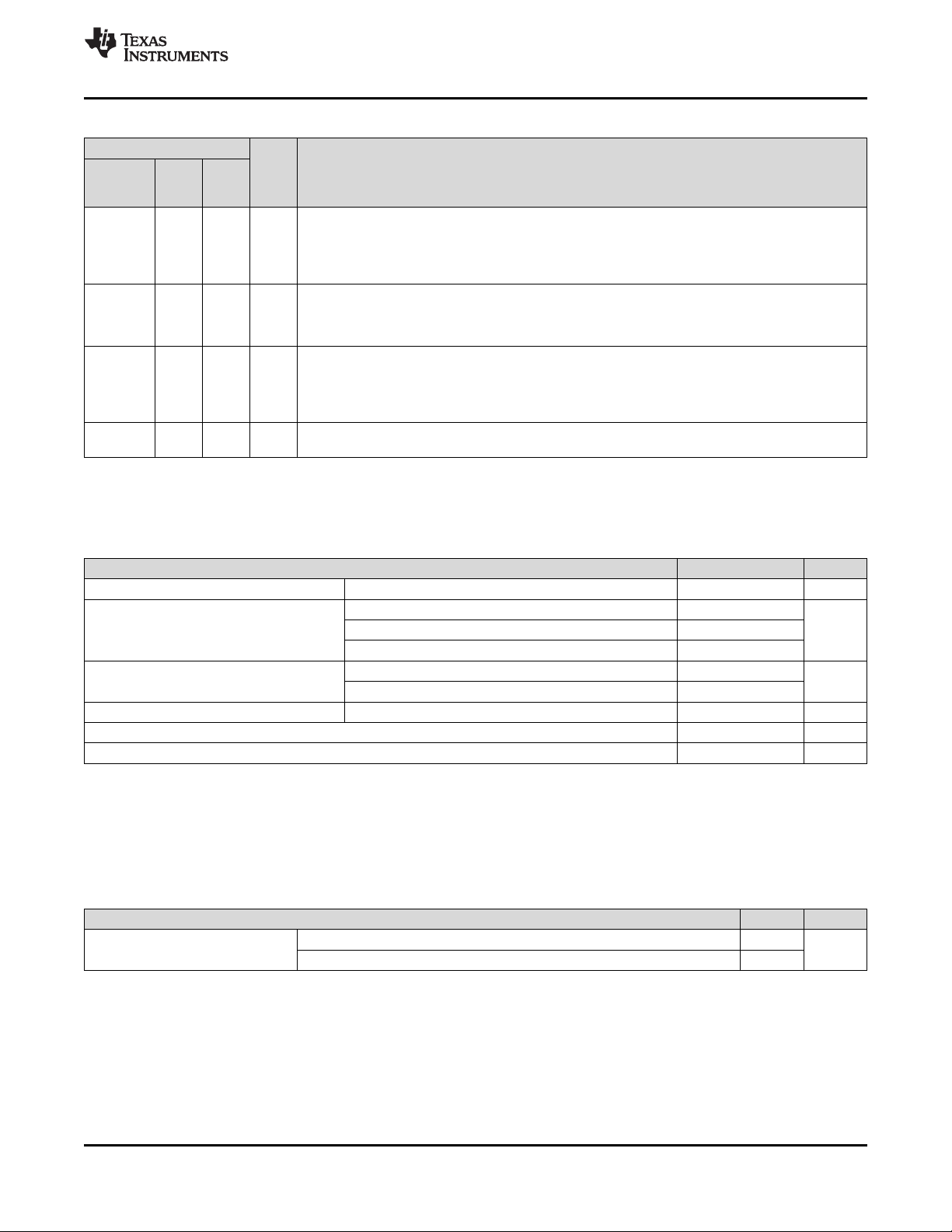
= 1.25 V –220 –200 –180 µA
RMS
= 1 V,
RMS
= 4 V –50 –42 –33 µA
VAOUT
= 2 V –38 –27 –12 µA
VAOUT
= 4 V –165 –150 –105 µA
VAOUT
= 2 V –250 –225 –150 µA
VAOUT
= 2 V –95 –80 –60 µA
VAOUT
–280 –255 –220 µA
= 15 kΩ 46 55 62 kHz
= 8.2 kΩ 86 102 118 kHz
= 7 V 95%
= –0.1 V –200 –100 µA
falling from 50 to –50 mV 175 ns
= 7.5 V,
ENA
–1 V
(2) Multiplier gain constant (k) is defined by:
Product Folder Links: UC1854 UC2854 UC3854
Submit Documentation FeedbackCopyright © 1998–2016, Texas Instruments Incorporated
7
Page 8

IAC, Am
μA
0
50
100
150
200
250
0 100 200 300 400 500
V =3VRMS
VA Out=1.25V
VA Out=2V
VA Out=3V
VA Out=5V
IAC, Am
μA
0
100
200
300
400
500
600
0 100 200 300 400 500
V
RMS
=1.5V
VA Out=1.25V
VA Out=2.5V
VA Out=3.5V
I , AACμ
Output
μA
0
100
200
300
400
500
600
0 100 200 300 400 500
600
700
800
Mult Out=1
Mult Out=2V
Mult Out=3V
Mult Out=0V
V =2V, VA Out=5V
RMS
R
SET
, k Ω
70%
75%
80%
85%
90%
95%
100%
1 10 100
Frequency
Phase
Margin
degrees
Gain
dB
-20
0
20
40
60
80
100
120
0.1 1 10 100 1000 10000
Frequency
Phase
Margin
degrees
Gain
dB
-20
0
20
40
60
80
100
120
0.1 1 10 100 1000 10000
UC1854,UC2854,UC3854
SLUS336A –JUNE 1998–REVISED DECEMBER 2016
7.6 Typical Characteristics
TA= TJ= 25°C
Figure 1. Current Amplifier Gain and Phase vs Frequency Figure 2. Voltage Amplifier Gain and Phase vs Frequency
www.ti.com
Figure 3. Gate-Drive Maximum Duty Cycle
8
Submit Documentation Feedback Copyright © 1998–2016, Texas Instruments Incorporated
Figure 5. Multiplier Output vs Multiplier Inputs
V
MULTOUT
Figure 4. Multiplier Output vs Voltage On MULTOUT
= 0 V
Product Folder Links: UC1854 UC2854 UC3854
V
MULTOUT
= 0 V
Figure 6. Multiplier Output vs Multiplier Inputs
Page 9
IAC, μA
μA
0
20
40
60
80
100
120
140
0
100 200 300 400 500
VRMS=5V
VA Out=5V
VA Out=1.5V
VA Out=3V
I ,AC A
A
0
20
40
60
80
100
120
140
160
0 100 200 300 400 500
V
RMS
=4V
VA Out=1.25V
VA Out=2V
VA Out=3V
VA Out=4V
VA Out=5V
μ
μ
www.ti.com
Typical Characteristics (continued)
TA= TJ= 25°C
UC1854,UC2854,UC3854
SLUS336A –JUNE 1998–REVISED DECEMBER 2016
V
MULTOUT
= 0 V
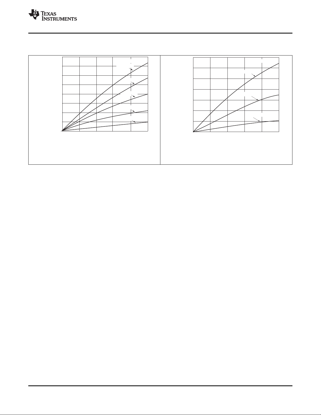
Figure 7. Multiplier Output vs Multiplier Inputs
V
MULTOUT
= 0 V
Figure 8. Multiplier Output vs Multiplier Inputs
Product Folder Links: UC1854 UC2854 UC3854
Submit Documentation FeedbackCopyright © 1998–2016, Texas Instruments Incorporated
9
Page 10
UC1854,UC2854,UC3854
SLUS336A –JUNE 1998–REVISED DECEMBER 2016
www.ti.com
8 Detailed Description
8.1 Overview
The UC3854 provides active power factor correction for systems that otherwise would draw non-sinusoidal
current from sinusoidal power lines. This device implements all the control functions necessary to build a power
supply capable of optimally using available power-line current while minimizing line current distortion.
The UC3854 uses average current-mode control to accomplish fixed-frequency current control with stability and
low distortion. The UC3854, with average current mode control, allows the boost stage to move between
continuous and discontinuous modes of operation without a performance change. Unlike peak current-mode,
average current control accurately maintains sinusoidal line current without slope compensation and with minimal
response to noise transients.
The UC3854 implements all the control functions necessary to build a power supply capable of optimally using
available power-line current while minimizing line-current distortion. The UC3854 contains a voltage amplifier, an
analog multiplier and divider, a current amplifier, and a fixed-frequency PWM. In addition, the UC3854 contains a
power MOSFET compatible gate driver, 7.5-V reference, line anticipator, load-enable comparator, low-supply
detector, and over-current comparator.
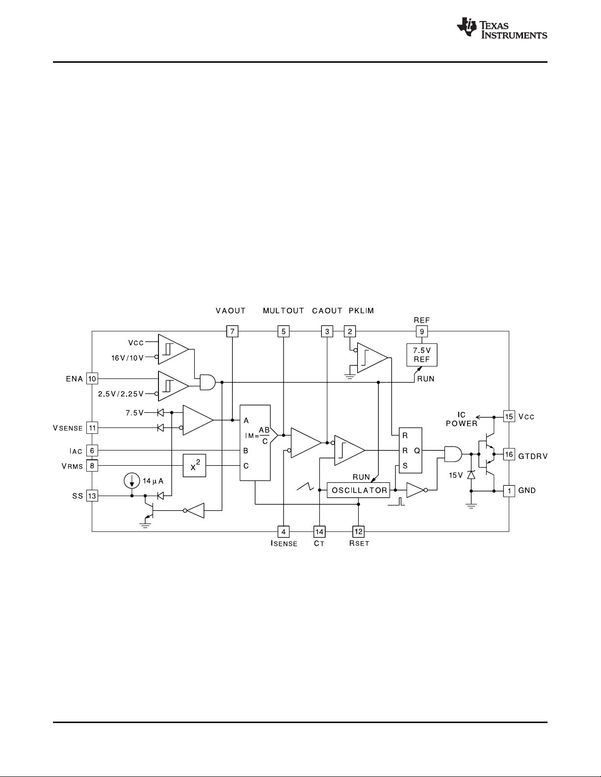
8.2 Functional Block Diagram
10
Submit Documentation Feedback Copyright © 1998–2016, Texas Instruments Incorporated
Product Folder Links: UC1854 UC2854 UC3854
Page 11

UC1854,UC2854,UC3854
www.ti.com
SLUS336A –JUNE 1998–REVISED DECEMBER 2016
8.3 Feature Description
The UC3854 integrated circuit contains all the circuits necessary to control a power factor corrector. The UC3854
is designed to implement average current mode control but is flexible enough to be used for a wide variety of
power topologies and control methods.
The top left corner, of the UC3854 block diagram, contains the under voltage lock out comparator and the enable
comparator. The output of both of these comparators must be true to allow the device to operate. The inverting
input to the voltage error amplifier is connected to pin VSENSE. The diodes shown around the voltage error
amplifier are intended to represent the functioning of the internal circuits rather than to show the actual devices.
The diodes shown in the block diagram are ideal diodes and indicate that the non-inverting input to the error
amplifier is connected to the 7.5-V DC reference voltage under normal operation but is also used for the soft-start
function. This configuration lets the voltage control loop begin operation before the output voltage has reached its
operating point and eliminates the turn-on overshoot which plagues many power supplies. The diode shown
between VSENSE and the inverting input of the error amplifier is also an ideal diode and is shown to eliminate
confusion about whether there might be an extra diode drop added to the reference or not. In the actual device
we do it with differential amplifiers. An internal current source is also provided for charging the soft-start timing
capacitor.
The output of the voltage error amplifier is available on pin VAOUT, of the UC3854, and it is also an input to the
multiplier. The other input to the multiplier is lAC, and this is the input for the programming wave shape from the
input rectifiers. This pin is held, internally, at 6 V and is a current input. The feedforward input is VFF, and its
value is squared before being fed into the divider input of the multiplier. The current (I
also used in the multiplier to limit the maximum output current. The output current of the multiplier is IMOand it
flows out of pin MULTOUT which is also connected to the non-inverting input of the current error amplifier.
The inverting input of the current amplifier is connected to pin ISENSE. The output of the current error amplifier
connects to the pulse width modulation (PWM) comparator where it is compared to the oscillator ramp on pin CT.
The oscillator and the comparator drive the set-reset flip-flop which, in turn, drives the high current output on pin
GTDRV. The output voltage is clamped internally to the UC3854 at 15 V so that power MOSFETs do not have
their gates over driven. An emergency peak current limit is provided on pin PKLMT and it shuts off the output
pulse when it is pulled slightly below ground. The reference voltage output is connected to pin VREF and the
input voltage is connected to pin VCC.
) from the RSET pin is
SET
8.4 Device Functional Modes
This device has no functional modes.
Product Folder Links: UC1854 UC2854 UC3854
Submit Documentation FeedbackCopyright © 1998–2016, Texas Instruments Incorporated
11
Page 12

UC1854,UC2854,UC3854
SLUS336A –JUNE 1998–REVISED DECEMBER 2016
www.ti.com
9 Application and Implementation
NOTE
Information in the following applications sections is not part of the TI component
specification, and TI does not warrant its accuracy or completeness. TI’s customers are
responsible for determining suitability of components for their purposes. Customers should
validate and test their design implementation to confirm system functionality.
9.1 Application Information
The UC3854 control IC is generally applicable to the control of AC-DC power supplies that require Active Power
Factor Correction off Universal AC line. Applications using this IC generally meets the Class D equipment input
current harmonics standards per EN61000-3-2. This standard applies to equipment with rated powers higher
than 75 W.
Performance of the UC3854 Power Factor correction IC in a 250-W application example has been evaluated
using a precision PFC and THD instrument. The result was a power factor of 0.999 and Total Harmonic
Distortion (THD) of 3.81%, measured to the 50th line frequency harmonic at nominal line and full load.
9.2 Typical Application
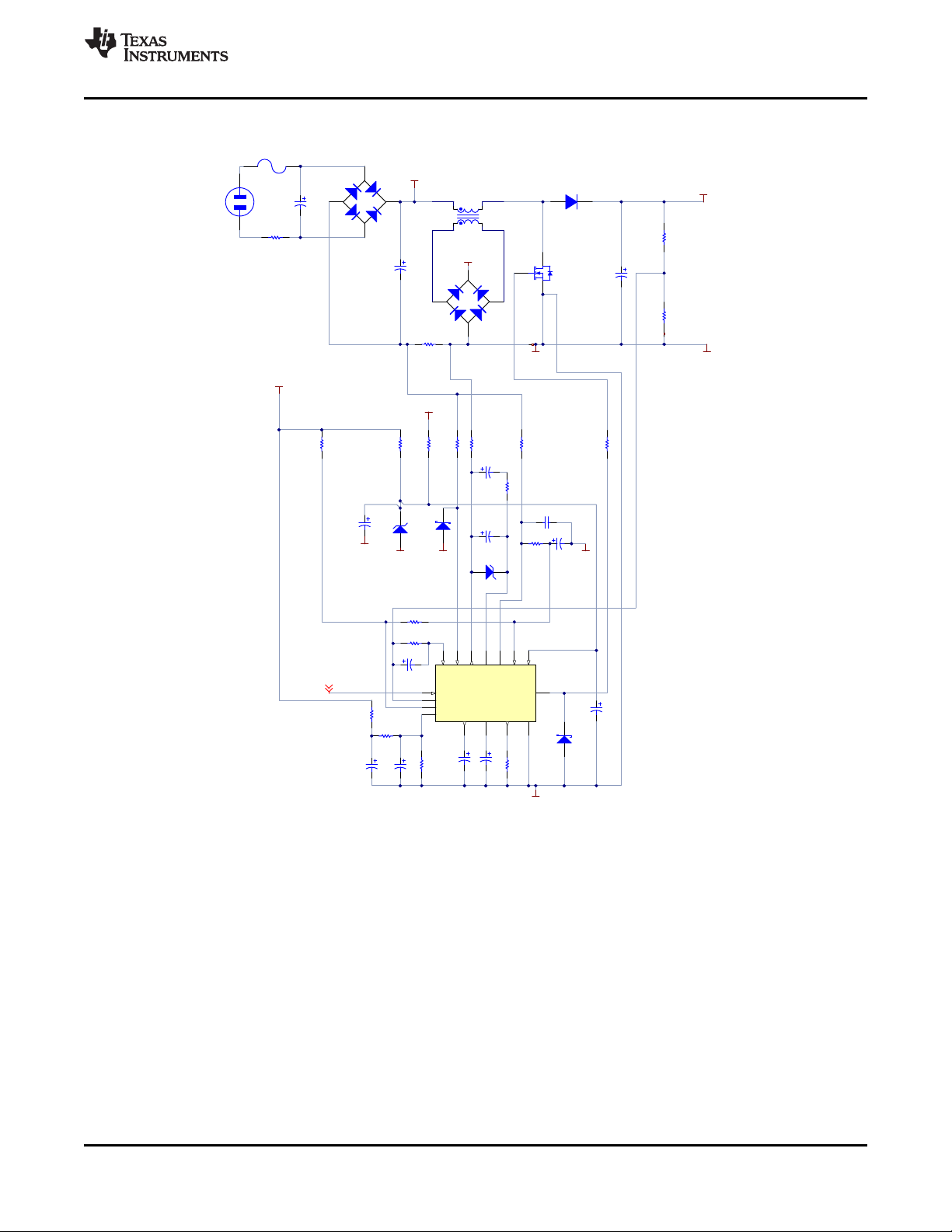
The circuit of Figure 9 shows a typical application of the UC3854 as a preregulator with high power factor and
efficiency. The assembly consists of two distinct parts: the control circuit centering on the UC3854 and the power
section.
The power section is a boost converter, with the inductor operating in continuous mode. In this mode, the duty
cycle is dependent on the ratio between input and output voltages; also, the input current has low switchingfrequency ripple, which means that the line noise is low. Furthermore, the output voltage must be higher than the
peak value of the highest expected AC line voltage, and all components must be rated accordingly.
At full load, this preregulator exhibits a power factor of 0.99 at any power line voltage from 80 V to 260 V
This same circuit is used at higher power levels with minor modifications to the power stage. See Optimizing
Performance in UC3854 Power Factor Correction Applications and UC3854 Controlled Power Factor Correction
Circuit Design.
RMS
.
12
Submit Documentation Feedback Copyright © 1998–2016, Texas Instruments Incorporated
Product Folder Links: UC1854 UC2854 UC3854
Page 13
GND
1
PKLMT
2
CA OUT
3
ISEN
4
MULT OUT
5
IAC
6
VAOUT
7
VRMS
8
REF
9
ENA
10
VSENSE
11
RSET
12
SS13CT
14
VCC
15
GT DRV
16
U1
GND
15k
R1
820pF
C1
470pF
C10
0.01uF
C4
20k
R6
0.5uF
C6
91k
R5
910k
R4
0.1uF
C11
D4
IN5820
0.1uF
C3
0.1uF
C5
D5
220k
R16
10k
R11
GND
62pF
C8
180k
R7
47nF
C7
24K
R8620pF
C9
4K
R10
4K
R9
D6
GND
100
R18
100uF
C2
10
R17
GND
GND
910K
R13
30K
3W
R15
1K6
R12
ENA
Vrec
Vcc
6A
t°
~
+
~
-
1µF
~+~
-
0.25 Ohms
R14
450µF
10k
R3
0.1µF
UHV806
Vcc
Vrec
+Vout
GND
385 VDC Out
1mH
22V
D1
Isense
Multi_Out
511k
R19
GND
Copyright © 2016, Texas Instruments Incorporated
www.ti.com
Typical Application (continued)
UC1854,UC2854,UC3854
SLUS336A –JUNE 1998–REVISED DECEMBER 2016
Boost inductor is fabricated with ARNOLD MPP toroidal core part number A-438381-2, using a 55-turn primary and a
13-turn secondary.
Figure 9. 250-W Preregulator Application
Product Folder Links: UC1854 UC2854 UC3854
Submit Documentation FeedbackCopyright © 1998–2016, Texas Instruments Incorporated
13
Page 14
UC1854,UC2854,UC3854
SLUS336A –JUNE 1998–REVISED DECEMBER 2016
www.ti.com
Typical Application (continued)
9.2.1 Design Requirements
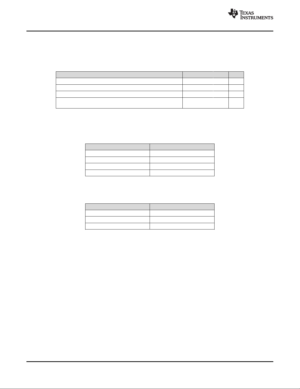
For this design example, use the parameters listed in Table 1 as the input parameters.
Table 1. Design Parameters
DESIGN PARAMETER MIN TYP MAX UNIT
V
V
f
P
ax)
9.2.2 Detailed Design Procedure
In the control section, the UC3854 provides PWM pulses (GTDRV) to the power MOSFET gate. The duty cycle
of this output is simultaneously controlled by four separate inputs to the chip.
RMS input voltage 80 260 V
IN
Output voltage 390 V
OUT
AC line frequency 47 65 Hz
Line
OUT(m
Maximum output power 250 W
Table 2. Output Duty Cycle
INPUT PIN FUNCTION
VSENSE Output DC voltage
IAC Line voltage waveform
ISENSE, MULTOUT Line current
VRMS RMS line voltage
RMS
Additional controls of an auxiliary nature are provided. They are intended to protect the switching power
MOSFETS from certain transient conditions.
Table 3. Additional Controls of the Output Duty Cycle
INPUT PIN FUNCTION
ENA Startup delay
SS Soft start
PKLMT Maximum current limit
9.2.2.1 Protection Inputs
ENA (Enable): The ENA input must reach 2.5 V before the VREF and GTDRV outputs are enabled. This
provides a means to shut down the gate in case of trouble, or to add a time delay at power up. A hysteresis gap
of 200 mV is provided at this terminal to prevent erratic operation. Undervoltage protection is provided directly at
VCC, where the on and off thresholds are 16 V and 10 V. If the ENA input is unused, it must be pulled up to V
CC
through a current-limiting resistor of 100 kΩ.
SS (Soft Start): The voltage at SS pin reduces the reference voltage used by the error amplifier to regulate the
output DC voltage. With SS open, the reference voltage is typically 7.5 V. An internal current source delivers
approximately 14 mA from SS. Thus a capacitor (CSS) connected between SS and ground charges linearly from
0 V to 7.5 V in [0.54 × CSS(µF)] s.
PKLMT (Peak Current Limit): Use PKLIM to establish the highest value of current to be controlled by the power
MOSFET. With the resistor divider values shown in Figure 9, the 0-V threshold at PKLIM is reached when the
voltage drop across the 0.25-Ω current-sense resistor is 7.5 V × 2 k / 10 k = 1.5 V, corresponding to 6 A. TI
recommends a bypass capacitor from PKLIM to GND to filter out very high frequency noise.
9.2.2.2 Control Inputs
VSENSE (Output DC Voltage Sense): The threshold voltage for the VSENSE input is 7.5 V and the input bias
current is typically 50 nA. The values shown in Figure 9 are for an output voltage of 400-V DC. In this circuit, the
voltage amplifier operates with a constant low-frequency gain for minimum output excursions. The 47-nF
feedback capacitor places a 15-Hz pole in the voltage loop that prevents 120-Hz ripple from propagating to the
input current.
14
Submit Documentation Feedback Copyright © 1998–2016, Texas Instruments Incorporated
Product Folder Links: UC1854 UC2854 UC3854
Page 15

T
SET
1.25
F R=´
MAX
MULT
MAX
I 4 k
0.25
- ´
= = -
W
MAX
MULT
3.75 V
15 k
-
= = -
MAX
MULT
SET
3.75 V
R
-
=
AC
REF
R
=
=
pk
AC
ACpk
V
260VAC 2
I 400 A
´
= = =
m
UC1854,UC2854,UC3854
www.ti.com
SLUS336A –JUNE 1998–REVISED DECEMBER 2016
IAC (Line Waveform): To force the line current waveshape to follow the line voltage, a sample of the power line
voltage in waveform is introduced at IAC. This signal is multiplied by the output of the voltage amplifier in the
internal multiplier to generate a reference signal for the current control loop.
This input is not a voltage, but a current (hence IAC), and is set up by the 220-kΩ and 910-kΩ resistive divider
(see Figure 12). The voltage at IAC is internally held at 6 V, and the two resistors are chosen so that the current
flowing into IAC varies from zero (at each zero-crossing) to about 400 µA at the peak of the waveshape. The
following formulas are used to calculate these resistors:
where
• VPKis the peak line voltage (2)
(3)
ISENSE and MULTOUT (Line Current): The voltage drop across the 0.25-Ω current-sense resistor is applied to
ISENSE and MULTOUT as shown. The current-sense amplifier also operates with high low-frequency gain, but
unlike the voltage amplifier, it is set up to give the current-control loop a very wide bandwidth. This bandwidth
enables the line current to follow the line voltage as closely as possible. In the present example, this amplifier
has a zero at about 500 Hz, and a gain of about 18 dB thereafter.
VRMS (RMS Line Voltage): An important feature of the UC3854 preregulator is that it operates with a three-toone range of input line voltages, covering everything from low line in the US (85 VAC) to high line in Europe (255
VAC). This is done using line feedforward, which keeps the input power constant with varying input voltage
(assuming constant load power). To do this, the multiplier divides the line current by the square of the RMS value
of the line voltage. The voltage applied to VRMS, proportional to the average of the rectified line voltage and
proportional to the RMS value, is squared in the UC3854, and then used as a divisor by the multiplier block. The
multiplier output, at MULTOUT, is a current that increases with the current at IAC and the voltage at VAOUT, and
decreases with the square of the voltage at VRMS.
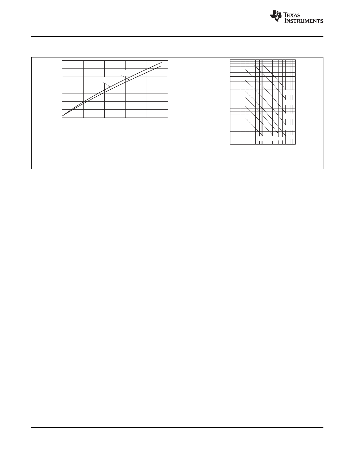
PWM Frequency: The PWM oscillator frequency in Figure 9 is 100 kHz. This value is determined by CTat pin CT
and R
at pin RSET. R
SET
must be chosen first because it affects the maximum value of I
SET
according to the
MULT
equation Equation 4.
This effectively sets a maximum PWM-controlled current. With R
Also note that the multiplier output current never exceeds twice IAC.
With the 4-kΩ resistor from MULTOUT to the 0.25-Ω current-sense resistor, the maximum current in the current-
sense resistor is:
Having thus selected R
resistor, calculate CTfor the desired PWM oscillator frequency from Equation 7.
(4)
= 15 k,
SET
(5)
(6)
, the current sense resistor, and the resistor from MULTOUT to the current sense
SET
(7)
Submit Documentation FeedbackCopyright © 1998–2016, Texas Instruments Incorporated
Product Folder Links: UC1854 UC2854 UC3854
15
Page 16
R , k
SET
Ω
kHz
10
100
1000
1
10
100
100pF
200pF
5nF
10nF
3nF
500pF
2nF
1nF
Load Capacitance, μF
0
100
200
300
400
500
600
700
0 0.01 0.02 0.03 0.04 0.05
Rise Time
Fall Time
UC1854,UC2854,UC3854
SLUS336A –JUNE 1998–REVISED DECEMBER 2016
9.2.3 Application Curves
www.ti.com
Figure 10. Gate-Drive Rise and Fall Time
Figure 11. Oscillator Frequency vs R
SET
10 Power Supply Recommendations
Bypass the VCC pin directly to the GND pin, using a ceramic capacitor of at least 0.1 µF. This bypass capacitor
absorbs supply current spikes required to charge external MOSFET gate capacitances.
VCC must be connected to a stable source that can deliver at least 20 mA. The VCC supply must exceed the
VCC turnon threshold to start switching operation and must remain above the VCC turnoff threshold for normal
operation.
A secondary winding on the PFC boost inductor can be used to deliver a regulated auxiliary bias supply with few
external components as shown in Figure 12. Unlike more conventional and unregulated single diode or bridge
rectifier techniques, this approach uses two diodes in a full wave configuration. This arrangement develops two
separate voltages across capacitors C1 and C2 each with 120-Hz components. However, when these two are
summed at capacitor C3, the line variations are cancelled, and a regulated auxiliary bias is obtained. The number
of turns on the secondary winding adjusts the bias supply voltage.
A bootstrap resistor and storage capacitor must be added, as shown in Figure 12 when VCCis obtained from a
PFC boost inductor auxiliary winding. These parts must be added to ensure the UC3854 controller has sufficient
VCC voltage to start up and operate through the soft-start process until sufficient voltage is available from the
auxiliary winding.
11 Layout
11.1 Layout Guidelines
Figure 12 and Figure 13 show good layout practice. The timing capacitor (C1) and bypass capacitors for VCC
and VREF (C3 and C5) must be connected directly from their respective pins to GND through the shortest route.
Ensure that the ISEN and MULTOUT pins do not drop more than 0.5 V below the GND pin; accomplished by
connecting a Schottky diode (D6) between GND and MULTOUT pins. The local controller GND must be
connected to the power circuit at a single point between the source of the power MOSFET and the current sense
resistor (R14). The power trace running between the power MOSFET source and current sense resistor (R14)
must be kept short. Traces from the upper terminals of R9 and R10 must run directly to each side of the current
sense resistor and not be shared with any other signal.
To minimize the possiblity of interference caused by magnetic coupling from the boost inductor, the device must
be located at least 1 in. away from the boost inductor. TI recommends the device not be placed underneath
magnetic elements.
16
Submit Documentation Feedback Copyright © 1998–2016, Texas Instruments Incorporated
Product Folder Links: UC1854 UC2854 UC3854
and C
T
Page 17

www.ti.com
11.2 Layout Example
UC1854,UC2854,UC3854
SLUS336A –JUNE 1998–REVISED DECEMBER 2016
Figure 12. Layout Diagram (Top View)
Figure 13. Layout Diagram (Bottom View)
Product Folder Links: UC1854 UC2854 UC3854
Submit Documentation FeedbackCopyright © 1998–2016, Texas Instruments Incorporated
17
Page 18

UC1854,UC2854,UC3854
SLUS336A –JUNE 1998–REVISED DECEMBER 2016
www.ti.com
12 Device and Documentation Support
12.1 Documentation Support
12.1.1 Related Documentation
For related documentation see the following:
• Optimizing Performance in UC3854 Power Factor Correction Applications (SLUA172)
• UC3854 Controlled Power Factor Correction Circuit Design (SLUA144)
12.2 Related Links
The table below lists quick access links. Categories include technical documents, support and community
resources, tools and software, and quick access to sample or buy.
Table 4. Related Links
PARTS PRODUCT FOLDER SAMPLE & BUY
UC1854 Click here Click here Click here Click here Click here
UC2854 Click here Click here Click here Click here Click here
UC3854 Click here Click here Click here Click here Click here
TECHNICAL
DOCUMENTS
12.3 Receiving Notification of Documentation Updates
To receive notification of documentation updates, navigate to the device product folder on ti.com. In the upper
right corner, click on Alert me to register and receive a weekly digest of any product information that has
changed. For change details, review the revision history included in any revised document.
TOOLS &
SOFTWARE
SUPPORT &
COMMUNITY
12.4 Community Resources
The following links connect to TI community resources. Linked contents are provided "AS IS" by the respective
contributors. They do not constitute TI specifications and do not necessarily reflect TI's views; see TI's Terms of
Use.
TI E2E™ Online Community TI's Engineer-to-Engineer (E2E) Community. Created to foster collaboration
among engineers. At e2e.ti.com, you can ask questions, share knowledge, explore ideas and help
solve problems with fellow engineers.
Design Support TI's Design Support Quickly find helpful E2E forums along with design support tools and
contact information for technical support.
12.5 Trademarks
E2E is a trademark of Texas Instruments.
All other trademarks are the property of their respective owners.
12.6 Electrostatic Discharge Caution
These devices have limited built-in ESD protection. The leads should be shorted together or the device placed in conductive foam
during storage or handling to prevent electrostatic damage to the MOS gates.
12.7 Glossary
SLYZ022 — TI Glossary.
This glossary lists and explains terms, acronyms, and definitions.
13 Mechanical, Packaging, and Orderable Information
The following pages include mechanical, packaging, and orderable information. This information is the most
current data available for the designated devices. This data is subject to change without notice and revision of
this document. For browser-based versions of this data sheet, refer to the left-hand navigation.
18
Submit Documentation Feedback Copyright © 1998–2016, Texas Instruments Incorporated
Product Folder Links: UC1854 UC2854 UC3854
Page 19
PACKAGE OPTION ADDENDUM
www.ti.com
PACKAGING INFORMATION
Orderable part number Status
5962-9326101MEA Active Production CDIP (J) | 16 25 | TUBE No SNPB N/A for Pkg Type -55 to 125 5962-9326101ME
UC1854J Active Production CDIP (J) | 16 25 | TUBE No SNPB N/A for Pkg Type -55 to 125 UC1854J
UC1854J.A Active Production CDIP (J) | 16 25 | TUBE No SNPB N/A for Pkg Type -55 to 125 UC1854J
UC1854J883B Active Production CDIP (J) | 16 25 | TUBE No SNPB N/A for Pkg Type -55 to 125 5962-9326101ME
UC1854J883B.A Active Production CDIP (J) | 16 25 | TUBE No SNPB N/A for Pkg Type -55 to 125 5962-9326101ME
UC2854BJ Active Production CDIP (J) | 16 25 | TUBE No SNPB N/A for Pkg Type -40 to 85 UC2854BJ
UC2854BJ.A Active Production CDIP (J) | 16 25 | TUBE No SNPB N/A for Pkg Type -40 to 85 UC2854BJ
UC2854DW Active Production SOIC (DW) | 16 40 | TUBE Yes NIPDAU Level-2-260C-1 YEAR -40 to 85 UC2854DW
UC2854DW.A Active Production SOIC (DW) | 16 40 | TUBE Yes NIPDAU Level-2-260C-1 YEAR -40 to 85 UC2854DW
UC2854DWTR Active Production SOIC (DW) | 16 2000 | LARGE T&R Yes NIPDAU Level-2-260C-1 YEAR -40 to 85 UC2854DW
UC2854DWTR.A Active Production SOIC (DW) | 16 2000 | LARGE T&R Yes NIPDAU Level-2-260C-1 YEAR -40 to 85 UC2854DW
UC2854N Active Production PDIP (N) | 16 25 | TUBE Yes NIPDAU N/A for Pkg Type -40 to 85 UC2854N
UC2854N.A Active Production PDIP (N) | 16 25 | TUBE Yes NIPDAU N/A for Pkg Type -40 to 85 UC2854N
UC3854DW Active Production SOIC (DW) | 16 40 | TUBE Yes NIPDAU Level-2-260C-1 YEAR 0 to 70 UC3854DW
UC3854DW.A Active Production SOIC (DW) | 16 40 | TUBE Yes NIPDAU Level-2-260C-1 YEAR 0 to 70 UC3854DW
UC3854DWG4 Active Production SOIC (DW) | 16 40 | TUBE Yes NIPDAU Level-2-260C-1 YEAR 0 to 70 UC3854DW
UC3854DWTR Active Production SOIC (DW) | 16 2000 | LARGE T&R Yes NIPDAU Level-2-260C-1 YEAR 0 to 70 UC3854DW
UC3854DWTR-F Active Production SOIC (DW) | 16 2000 | LARGE T&R Yes NIPDAU Level-2-260C-1 YEAR 0 to 70 UC3854DW-F
UC3854DWTR-F.A Active Production SOIC (DW) | 16 2000 | LARGE T&R Yes NIPDAU Level-2-260C-1 YEAR 0 to 70 UC3854DW-F
UC3854DWTR.A Active Production SOIC (DW) | 16 2000 | LARGE T&R Yes NIPDAU Level-2-260C-1 YEAR 0 to 70 UC3854DW
UC3854DWTRG4 Active Production SOIC (DW) | 16 2000 | LARGE T&R Yes NIPDAU Level-2-260C-1 YEAR 0 to 70 UC3854DW
UC3854N Active Production PDIP (N) | 16 25 | TUBE Yes NIPDAU N/A for Pkg Type 0 to 70 UC3854N
UC3854N.A Active Production PDIP (N) | 16 25 | TUBE Yes NIPDAU N/A for Pkg Type 0 to 70 UC3854N
UC3854NG4 Active Production PDIP (N) | 16 25 | TUBE Yes NIPDAU N/A for Pkg Type 0 to 70 UC3854N
(1)
Material type
(2)
Package | Pins Package qty | Carrier RoHS
(3)
Lead finish/
Ball material
(4)
MSL rating/
Peak reflow
(5)
Op temp (°C) Part marking
UC1854J/883B
UC1854J/883B
UC1854J/883B
8-Jan-2026
(6)
A
A
A
Addendum-Page 1
Page 20

PACKAGE OPTION ADDENDUM
www.ti.com
(1)
Status: For more details on status, see our product life cycle.
8-Jan-2026
(2)
Material type: When designated, preproduction parts are prototypes/experimental devices, and are not yet approved or released for full production. Testing and final process, including without limitation quality assurance,
reliability performance testing, and/or process qualification, may not yet be complete, and this item is subject to further changes or possible discontinuation. If available for ordering, purchases will be subject to an additional
waiver at checkout, and are intended for early internal evaluation purposes only. These items are sold without warranties of any kind.
(3)
RoHS values: Yes, No, RoHS Exempt. See the TI RoHS Statement for additional information and value definition.
(4)
Lead finish/Ball material: Parts may have multiple material finish options. Finish options are separated by a vertical ruled line. Lead finish/Ball material values may wrap to two lines if the finish value exceeds the maximum
column width.
(5)
MSL rating/Peak reflow: The moisture sensitivity level ratings and peak solder (reflow) temperatures. In the event that a part has multiple moisture sensitivity ratings, only the lowest level per JEDEC standards is shown.
Refer to the shipping label for the actual reflow temperature that will be used to mount the part to the printed circuit board.
(6)
Part marking: There may be an additional marking, which relates to the logo, the lot trace code information, or the environmental category of the part.
Multiple part markings will be inside parentheses. Only one part marking contained in parentheses and separated by a "~" will appear on a part. If a line is indented then it is a continuation of the previous line and the two
combined represent the entire part marking for that device.
Important Information and Disclaimer:The information provided on this page represents TI's knowledge and belief as of the date that it is provided. TI bases its knowledge and belief on information provided by third parties, and
makes no representation or warranty as to the accuracy of such information. Efforts are underway to better integrate information from third parties. TI has taken and continues to take reasonable steps to provide representative
and accurate information but may not have conducted destructive testing or chemical analysis on incoming materials and chemicals. TI and TI suppliers consider certain information to be proprietary, and thus CAS numbers
and other limited information may not be available for release.
In no event shall TI's liability arising out of such information exceed the total purchase price of the TI part(s) at issue in this document sold by TI to Customer on an annual basis.
OTHER QUALIFIED VERSIONS OF UC1854, UC2854, UC2854BM, UC3854 :
Catalog : UC3854, UC2854B
•
Enhanced Product : UC2854B-EP
•
Military : UC2854M, UC1854
•
NOTE: Qualified Version Definitions:
Catalog - TI's standard catalog product
•
Addendum-Page 2
Page 21

PACKAGE OPTION ADDENDUM
www.ti.com
Enhanced Product - Supports Defense, Aerospace and Medical Applications
•
Military - QML certified for Military and Defense Applications
•
8-Jan-2026
Addendum-Page 3
Page 22
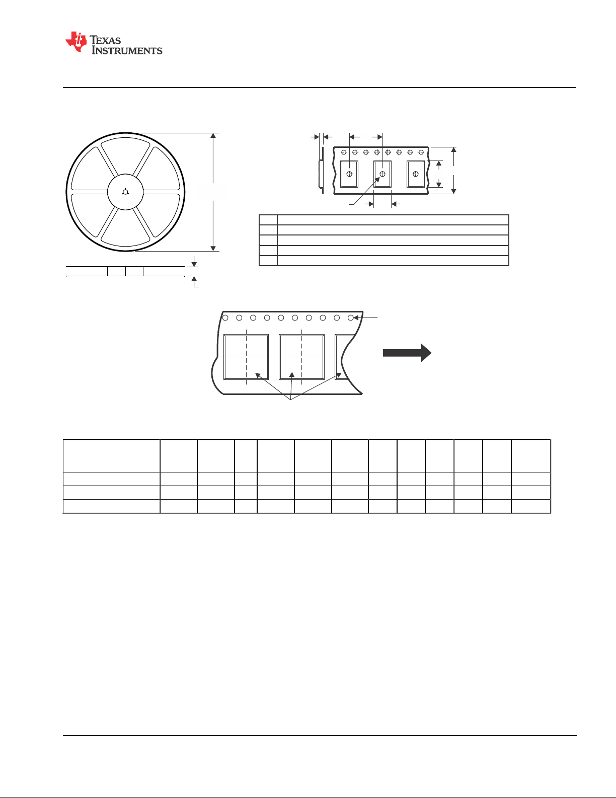
PACKAGE MATERIALS INFORMATION
Reel Width (W1)
REEL DIMENSIONS
A0
B0
K0
W
Dimension designed to accommodate the component length
Dimension designed to accommodate the component thickness
Overall width of the carrier tape
Pitch between successive cavity centers
Dimension designed to accommodate the component width
TAPE DIMENSIONS
K0 P1
B0
W
A0
Cavity
QUADRANT ASSIGNMENTS FOR PIN 1 ORIENTATION IN TAPE
Pocket Quadrants
Sprocket Holes
Q1
Q1Q2 Q2
Q3 Q3Q4 Q4
User Direction of Feed
P1
Reel
Diameter
www.ti.com 25-Jul-2025
TAPE AND REEL INFORMATION
*All dimensions are nominal
UC2854DWTR SOIC DW 16 2000 330.0 16.4 10.75 10.7 2.7 12.0 16.0 Q1
UC3854DWTR SOIC DW 16 2000 330.0 16.4 10.75 10.7 2.7 12.0 16.0 Q1
UC3854DWTR-F SOIC DW 16 2000 330.0 16.4 10.75 10.7 2.7 12.0 16.0 Q1
Device Package
Type
Package
Drawing
Pins SPQ Reel
Diameter
(mm)
Reel
Width
W1 (mm)
A0
(mm)B0(mm)K0(mm)P1(mm)W(mm)
Pin1
Quadrant
Pack Materials-Page 1
Page 23
PACKAGE MATERIALS INFORMATION
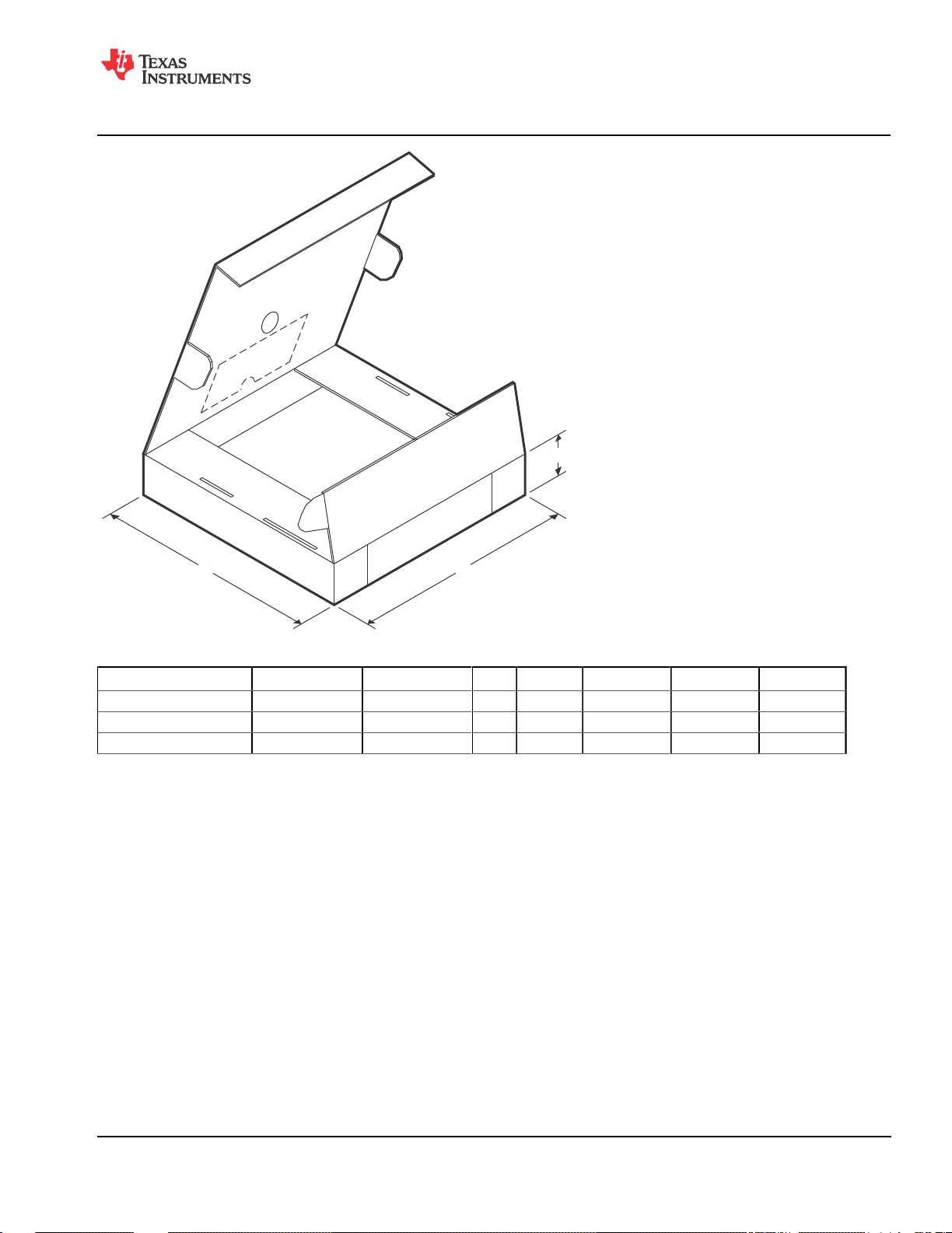
TAPE AND REEL BOX DIMENSIONS
Width (mm)
W
L
H
www.ti.com 25-Jul-2025
*All dimensions are nominal
Device Package Type Package Drawing Pins SPQ Length (mm) Width (mm) Height (mm)
UC2854DWTR SOIC DW 16 2000 353.0 353.0 32.0
UC3854DWTR SOIC DW 16 2000 353.0 353.0 32.0
UC3854DWTR-F SOIC DW 16 2000 353.0 353.0 32.0
Pack Materials-Page 2
Page 24
PACKAGE MATERIALS INFORMATION
www.ti.com 25-Jul-2025
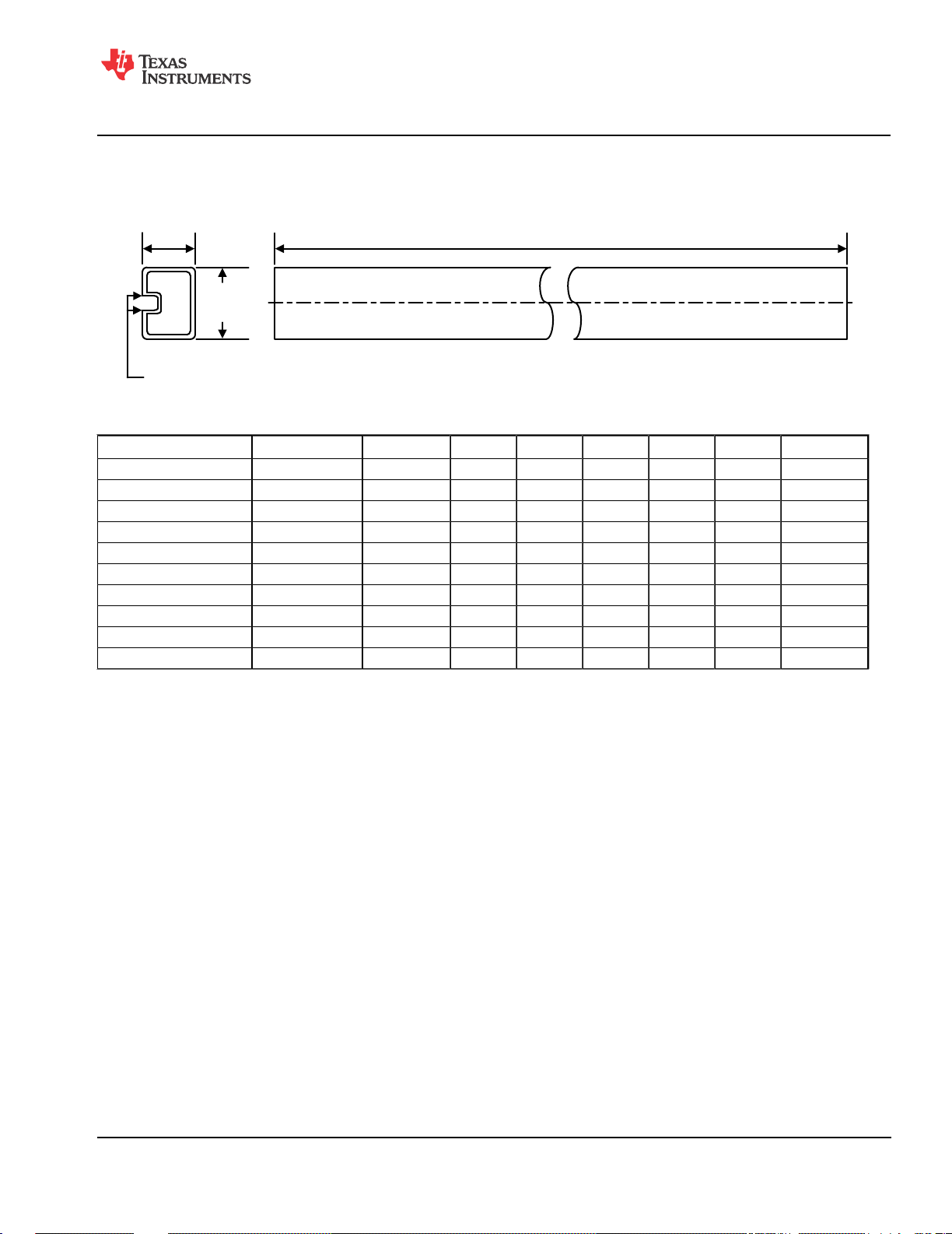
TUBE
T - Tube
height
W - Tube
width
B - Alignment groove width
*All dimensions are nominal
Device Package Name Package Type Pins SPQ L (mm) W (mm) T (µm) B (mm)
UC2854DW DW SOIC 16 40 507 12.83 5080 6.6
UC2854DW.A DW SOIC 16 40 507 12.83 5080 6.6
UC2854N N PDIP 16 25 506 13.97 11230 4.32
UC2854N.A N PDIP 16 25 506 13.97 11230 4.32
UC3854DW DW SOIC 16 40 507 12.83 5080 6.6
UC3854DW.A DW SOIC 16 40 507 12.83 5080 6.6
UC3854DWG4 DW SOIC 16 40 507 12.83 5080 6.6
UC3854N N PDIP 16 25 506 13.97 11230 4.32
UC3854N.A N PDIP 16 25 506 13.97 11230 4.32
UC3854NG4 N PDIP 16 25 506 13.97 11230 4.32
L - Tube length
Pack Materials-Page 3
Page 25

GENERIC PACKAGE VIEW
SOIC - 2.65 mm max heightDW 16
7.5 x 10.3, 1.27 mm pitch
This image is a representation of the package family, actual package may vary.
SMALL OUTLINE INTEGRATED CIRCUIT
Refer to the product data sheet for package details.
www.ti.com
4224780/A
Page 26
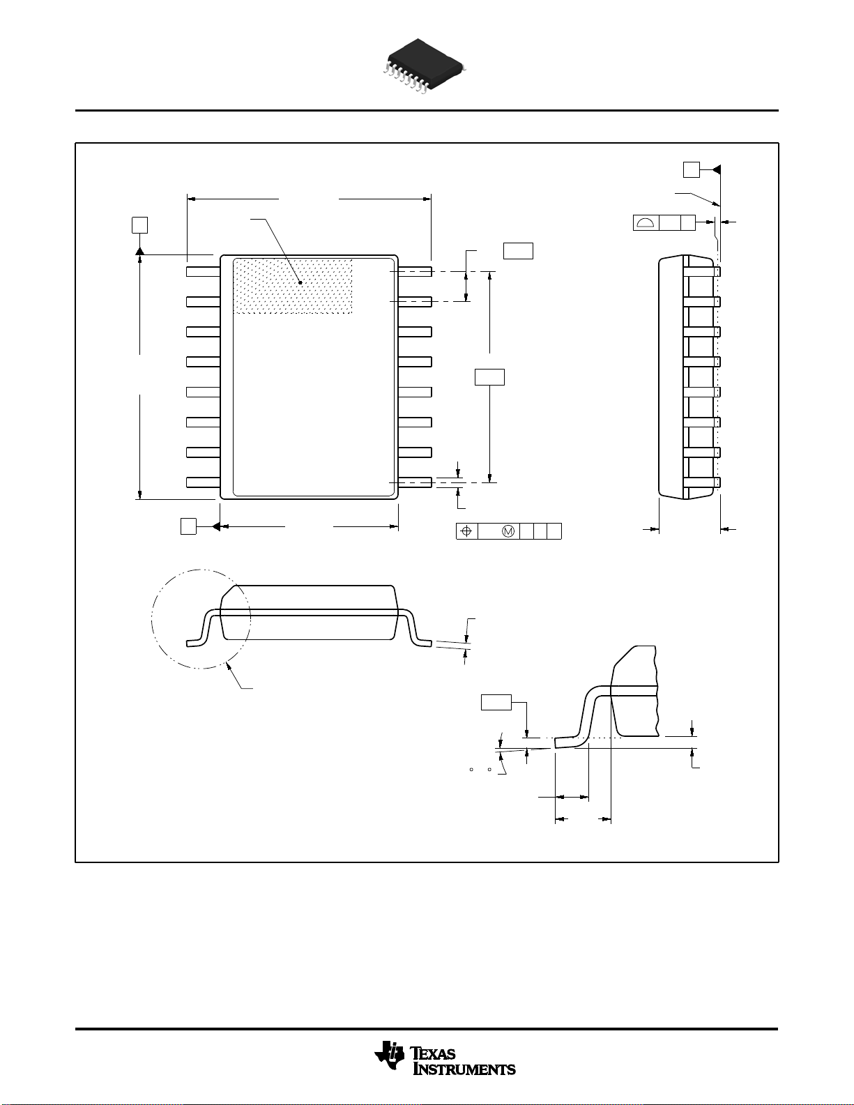
PACKAGE OUTLINE
A
10.5
10.1
NOTE 3
SCALE 1.500
10.63
TYP
9.97
PIN 1 ID
AREA
1
8
B
7.6
7.4
NOTE 4
16
9
14X 1.27
2X
8.89
0.51
16X
0.31
0.25 C A B
SOIC - 2.65 mm max heightDW0016A
SOIC
C
SEATING PLANE
0.1 C
2.65 MAX
0.33
TYP
0.10
SEE DETAIL A
GAGE PLANE
0 - 8
0.25
1.27
0.40
(1.4)
DETAIL A
TYPICAL
4220721/A 07/2016
NOTES:
1. All linear dimensions are in millimeters. Dimensions in parenthesis are for reference only. Dimensioning and tolerancing
per ASME Y14.5M.
2. This drawing is subject to change without notice.
3. This dimension does not include mold flash, protrusions, or gate burrs. Mold flash, protrusions, or gate burrs shall not
exceed 0.15 mm, per side.
4. This dimension does not include interlead flash. Interlead flash shall not exceed 0.25 mm, per side.
5. Reference JEDEC registration MS-013.
0.3
0.1
www.ti.com
Page 27
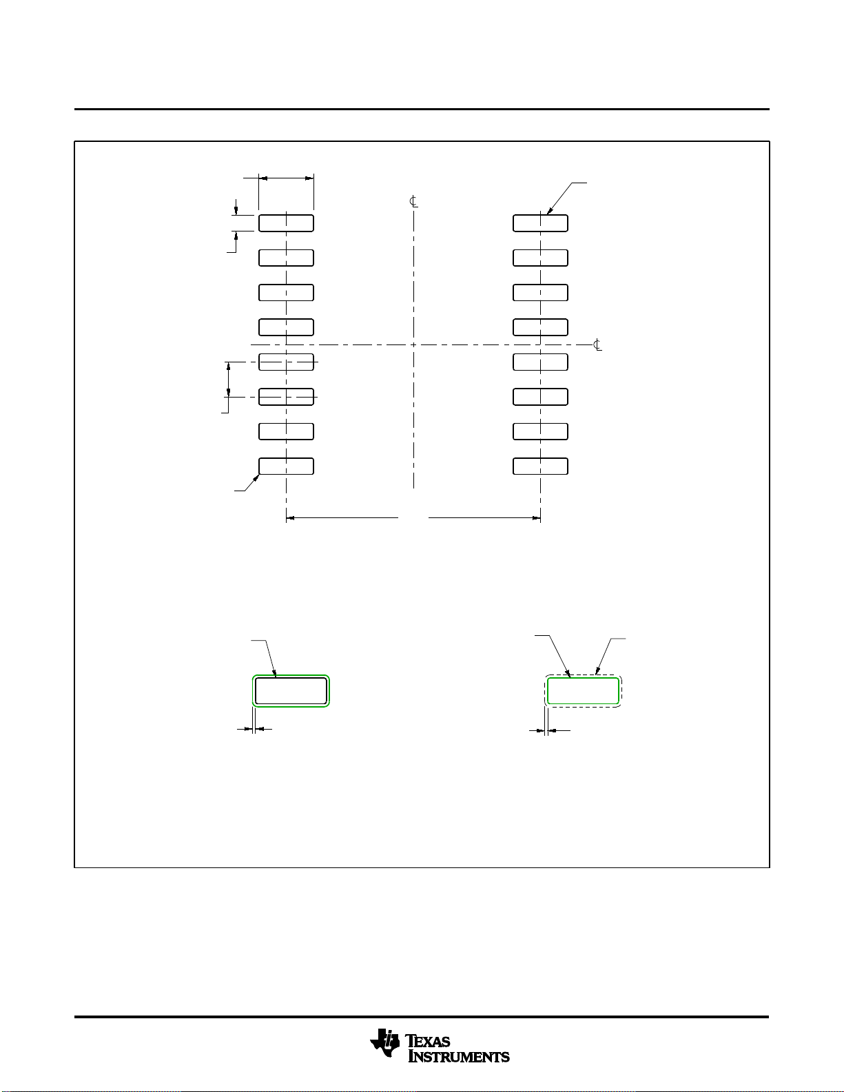
EXAMPLE BOARD LAYOUT
SOIC - 2.65 mm max heightDW0016A
SOIC
16X (2)
16X (0.6)
14X (1.27)
R0.05 TYP
SYMM
1
8
(9.3)
SEE
DETAILS
16
SYMM
9
LAND PATTERN EXAMPLE
SCALE:7X
METAL
0.07 MAX
ALL AROUND
NON SOLDER MASK
DEFINED
SOLDER MASK
OPENING
SOLDER MASK
OPENING
0.07 MIN
ALL AROUND
SOLDER MASK
DEFINED
SOLDER MASK DETAILS
NOTES: (continued)
6. Publication IPC-7351 may have alternate designs.
7. Solder mask tolerances between and around signal pads can vary based on board fabrication site.
METAL
4220721/A 07/2016
www.ti.com
Page 28
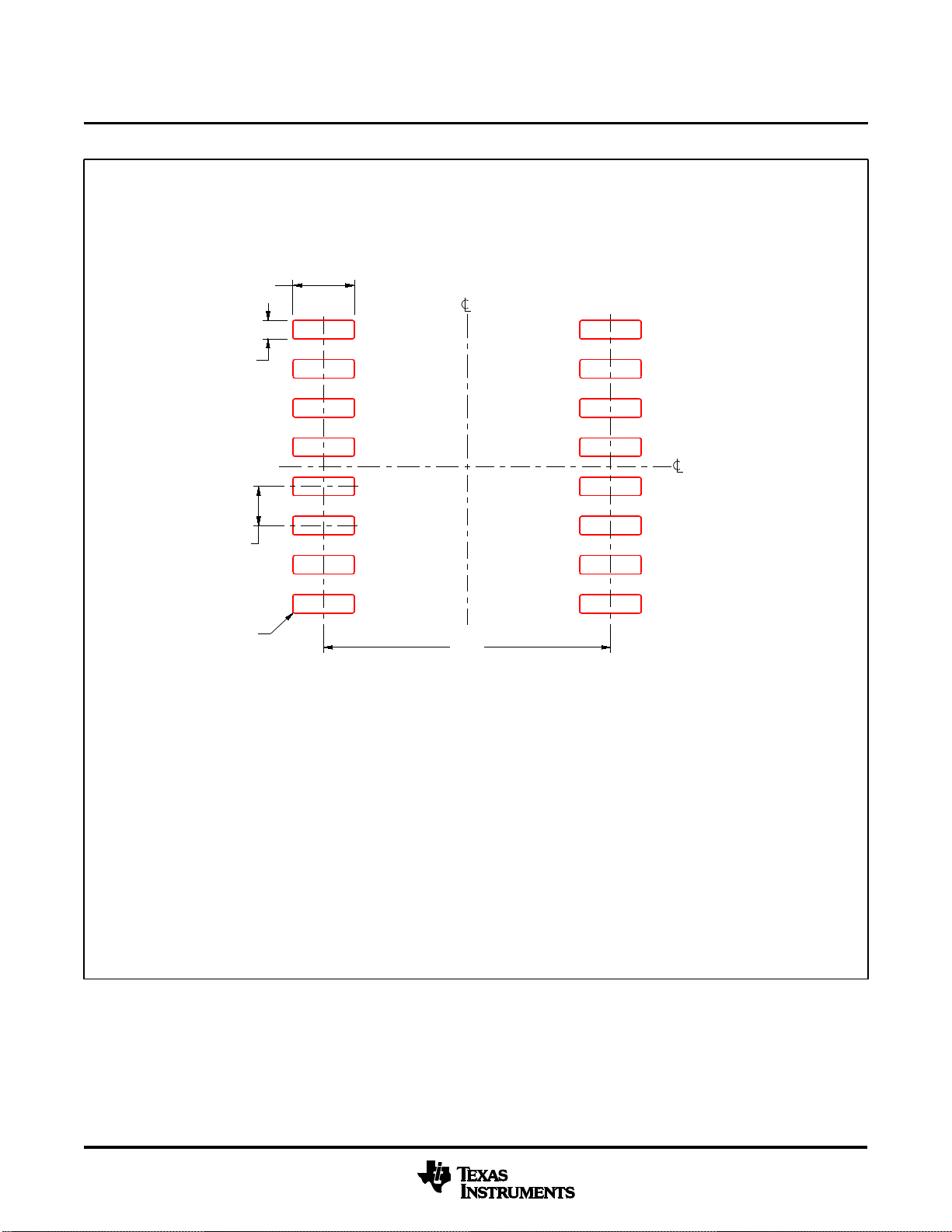
EXAMPLE STENCIL DESIGN
SOIC - 2.65 mm max heightDW0016A
SOIC
16X (2)
16X (0.6)
14X (1.27)
R0.05 TYP
SYMM
1
8
(9.3)
16
SYMM
9
SOLDER PASTE EXAMPLE
BASED ON 0.125 mm THICK STENCIL
NOTES: (continued)
8. Laser cutting apertures with trapezoidal walls and rounded corners may offer better paste release. IPC-7525 may have alternate
design recommendations.
9. Board assembly site may have different recommendations for stencil design.
SCALE:7X
4220721/A 07/2016
www.ti.com
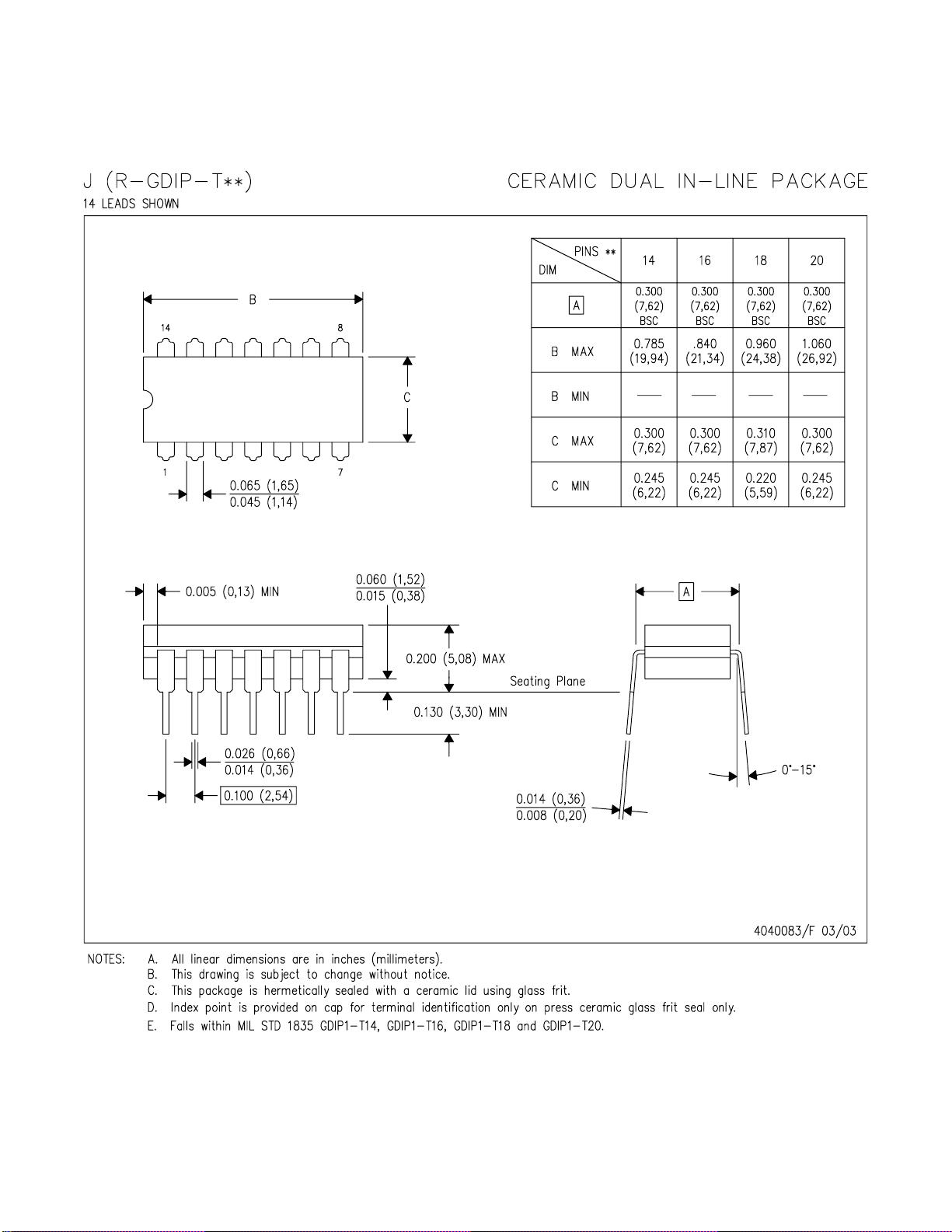
Page 29
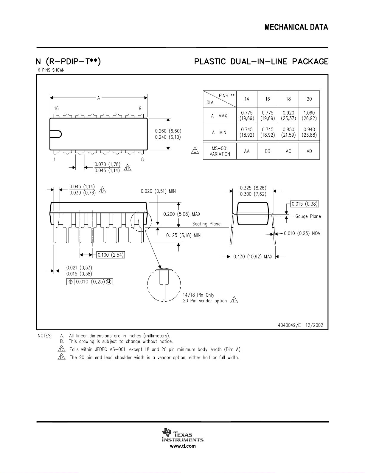
Page 30
Page 31

IMPORTANT NOTICE AND DISCLAIMER
TI PROVIDES TECHNICAL AND RELIABILITY DATA (INCLUDING DATASHEETS), DESIGN RESOURCES (INCLUDING REFERENCE
DESIGNS), APPLICATION OR OTHER DESIGN ADVICE, WEB TOOLS, SAFETY INFORMATION, AND OTHER RESOURCES “AS IS”
AND WITH ALL FAULTS, AND DISCLAIMS ALL WARRANTIES, EXPRESS AND IMPLIED, INCLUDING WITHOUT LIMITATION ANY
IMPLIED WARRANTIES OF MERCHANTABILITY, FITNESS FOR A PARTICULAR PURPOSE OR NON-INFRINGEMENT OF THIRD
PARTY INTELLECTUAL PROPERTY RIGHTS.
These resources are intended for skilled developers designing with TI products. You are solely responsible for (1) selecting the appropriate
TI products for your application, (2) designing, validating and testing your application, and (3) ensuring your application meets applicable
standards, and any other safety, security, regulatory or other requirements.
These resources are subject to change without notice. TI grants you permission to use these resources only for development of an
application that uses the TI products described in the resource. Other reproduction and display of these resources is prohibited. No license
is granted to any other TI intellectual property right or to any third party intellectual property right. TI disclaims responsibility for, and you fully
indemnify TI and its representatives against any claims, damages, costs, losses, and liabilities arising out of your use of these resources.
TI’s products are provided subject to TI’s Terms of Sale, TI’s General Quality Guidelines, or other applicable terms available either on
ti.com or provided in conjunction with such TI products. TI’s provision of these resources does not expand or otherwise alter TI’s applicable
warranties or warranty disclaimers for TI products. Unless TI explicitly designates a product as custom or customer-specified, TI products
are standard, catalog, general purpose devices.
TI objects to and rejects any additional or different terms you may propose.
IMPORTANT NOTICE
Copyright © 2026, Texas Instruments Incorporated
Last updated 10/2025
 Loading...