

Page 1
Features
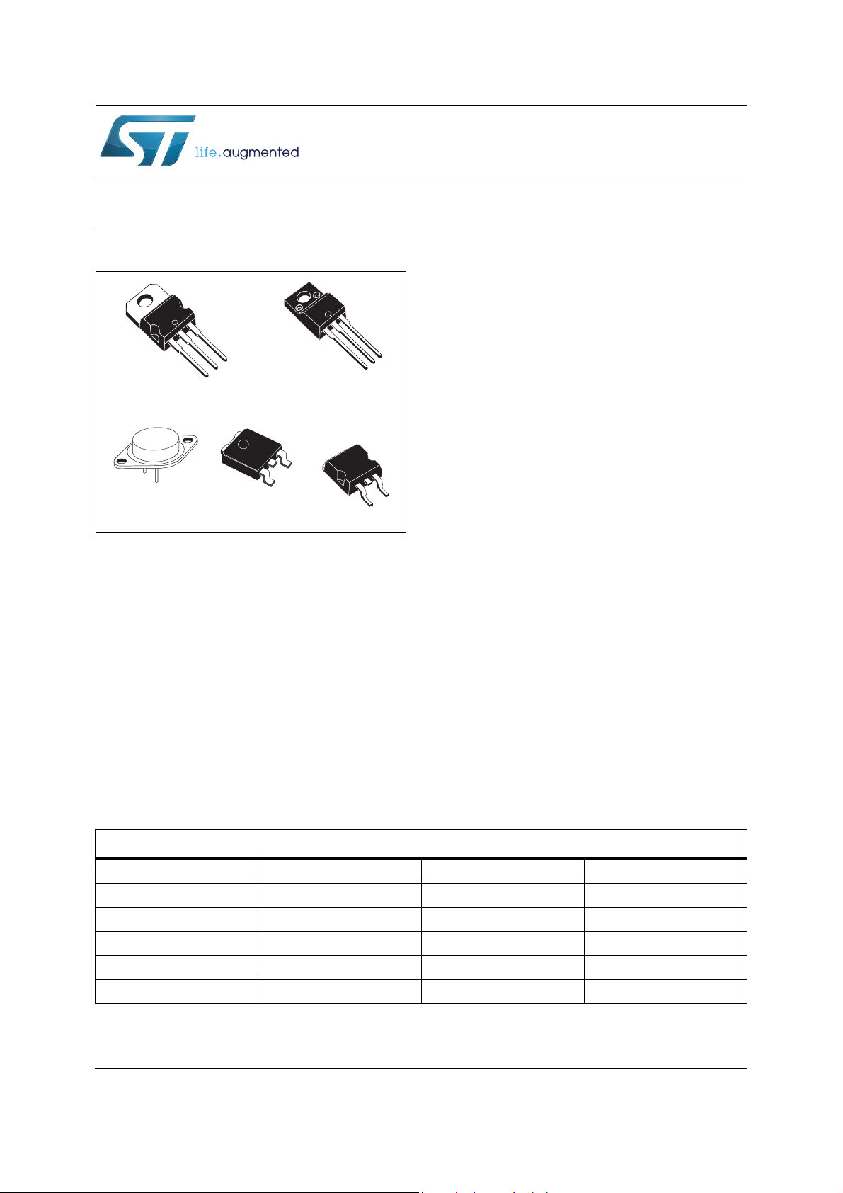
TO-220FP
TO-3
TO-220
D²PAK
DPAK
Output current up to 1.5 A
Output voltages of 5; 6; 8; 8.5; 9; 12; 15; 18;
24 V
Thermal overload protection
Short circuit protection
Output transition SOA protection
2 % output voltage tolerance (A version)
Guaranteed in extended temperature range
(A version)
L78xx, L78xxC,
L78xxAB, L78xxAC
Positive voltage regulator ICs
Datasheet - production data
Description
The L78xx series of three-terminal positive
regulators is available in TO-220, TO-220FP, TO3, D²PAK and DPAK packages and several fixed
output voltages, making it useful in a wide range
of applications.
These regulators can provide local on-card
regulation, eliminating the distribution problems
associated with single point regulation. Each type
employs internal current limiting, thermal shutdown and safe area protection, making it
essentially indestructible. If adequate heat sinking
is provided, they can deliver over 1 A output
current. Although designed primarily as fixed
voltage regulators, these devices can be used
with external components to obtain adjustable
voltage and currents.
Table 1. Device summary
Part numbers
L7805 L7806AC L7809AB L7815AB
L7805C L7808C L7809AC L7815AC
L7805AB L7808AB L7812C L7818C
L7805AC L7808AC L7812AB L7824C
L7806C L7885C L7812AC L7824AB
L7806AB L7809C L7815C L7824AC
March 2013 DocID2143 Rev 31 1/57
This is information on a product in full production.
www.st.com
57
Page 2

Contents L78xx, L78xxC, L78xxAB, L78xxAC
Contents
1 Diagram . . . . . . . . . . . . . . . . . . . . . . . . . . . . . . . . . . . . . . . . . . . . . . . . . . . 5
2 Pin configuration . . . . . . . . . . . . . . . . . . . . . . . . . . . . . . . . . . . . . . . . . . . 6
3 Maximum ratings . . . . . . . . . . . . . . . . . . . . . . . . . . . . . . . . . . . . . . . . . . . . 7
4 Test circuits . . . . . . . . . . . . . . . . . . . . . . . . . . . . . . . . . . . . . . . . . . . . . . . . 8
5 Electrical characteristics . . . . . . . . . . . . . . . . . . . . . . . . . . . . . . . . . . . . . 9
6 Application information . . . . . . . . . . . . . . . . . . . . . . . . . . . . . . . . . . . . . 28
6.1 Design consideration . . . . . . . . . . . . . . . . . . . . . . . . . . . . . . . . . . . . . . . . 28
7 Typical performance . . . . . . . . . . . . . . . . . . . . . . . . . . . . . . . . . . . . . . . . 37
8 Package mechanical data . . . . . . . . . . . . . . . . . . . . . . . . . . . . . . . . . . . . 39
9 Order codes . . . . . . . . . . . . . . . . . . . . . . . . . . . . . . . . . . . . . . . . . . . . . . 54
10 Revision history . . . . . . . . . . . . . . . . . . . . . . . . . . . . . . . . . . . . . . . . . . . 56
2/57 DocID2143 Rev 31
Page 3

L78xx, L78xxC, L78xxAB, L78xxAC List of tables
List of tables
Table 1. Device summary . . . . . . . . . . . . . . . . . . . . . . . . . . . . . . . . . . . . . . . . . . . . . . . . . . . . . . . . . . 1
Table 2. Absolute maximum ratings . . . . . . . . . . . . . . . . . . . . . . . . . . . . . . . . . . . . . . . . . . . . . . . . . . 7
Table 3. Thermal data. . . . . . . . . . . . . . . . . . . . . . . . . . . . . . . . . . . . . . . . . . . . . . . . . . . . . . . . . . . . . 7
Table 4. Electrical characteristics of L7805 . . . . . . . . . . . . . . . . . . . . . . . . . . . . . . . . . . . . . . . . . . . . 9
Table 5. Electrical characteristics of L7805A . . . . . . . . . . . . . . . . . . . . . . . . . . . . . . . . . . . . . . . . . . 10
Table 6. Electrical characteristics of L7806A . . . . . . . . . . . . . . . . . . . . . . . . . . . . . . . . . . . . . . . . . . 11
Table 7. Electrical characteristics of L7808A . . . . . . . . . . . . . . . . . . . . . . . . . . . . . . . . . . . . . . . . . . 12
Table 8. Electrical characteristics of L7809A . . . . . . . . . . . . . . . . . . . . . . . . . . . . . . . . . . . . . . . . . . 13
Table 9. Electrical characteristics of L7812A . . . . . . . . . . . . . . . . . . . . . . . . . . . . . . . . . . . . . . . . . . 14
Table 10. Electrical characteristics of L7815A . . . . . . . . . . . . . . . . . . . . . . . . . . . . . . . . . . . . . . . . . . 15
Table 11. Electrical characteristics of L7824A . . . . . . . . . . . . . . . . . . . . . . . . . . . . . . . . . . . . . . . . . . 16
Table 12. Electrical characteristics of L7805C . . . . . . . . . . . . . . . . . . . . . . . . . . . . . . . . . . . . . . . . . . 17
Table 13. Electrical characteristics of L7806C . . . . . . . . . . . . . . . . . . . . . . . . . . . . . . . . . . . . . . . . . . 18
Table 14. Electrical characteristics of L7808C . . . . . . . . . . . . . . . . . . . . . . . . . . . . . . . . . . . . . . . . . . 19
Table 15. Electrical characteristics of L7885C . . . . . . . . . . . . . . . . . . . . . . . . . . . . . . . . . . . . . . . . . . 20
Table 16. Electrical characteristics of L7809C . . . . . . . . . . . . . . . . . . . . . . . . . . . . . . . . . . . . . . . . . . 21
Table 17. Electrical characteristics of L7810C . . . . . . . . . . . . . . . . . . . . . . . . . . . . . . . . . . . . . . . . . . 22
Table 18. Electrical characteristics of L7812C . . . . . . . . . . . . . . . . . . . . . . . . . . . . . . . . . . . . . . . . . . 23
Table 19. Electrical characteristics of L7815C . . . . . . . . . . . . . . . . . . . . . . . . . . . . . . . . . . . . . . . . . . 24
Table 20. Electrical characteristics of L7818C . . . . . . . . . . . . . . . . . . . . . . . . . . . . . . . . . . . . . . . . . . 25
Table 21. Electrical characteristics of L7820C . . . . . . . . . . . . . . . . . . . . . . . . . . . . . . . . . . . . . . . . . . 26
Table 22. Electrical characteristics of L7824C . . . . . . . . . . . . . . . . . . . . . . . . . . . . . . . . . . . . . . . . . . 27
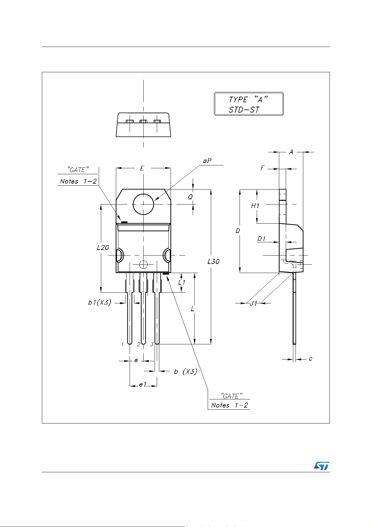
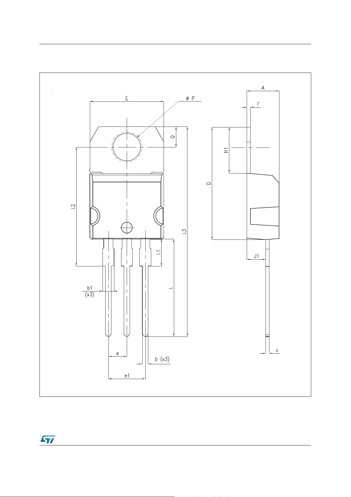
Table 23. TO-220 mechanical data . . . . . . . . . . . . . . . . . . . . . . . . . . . . . . . . . . . . . . . . . . . . . . . . . . 39
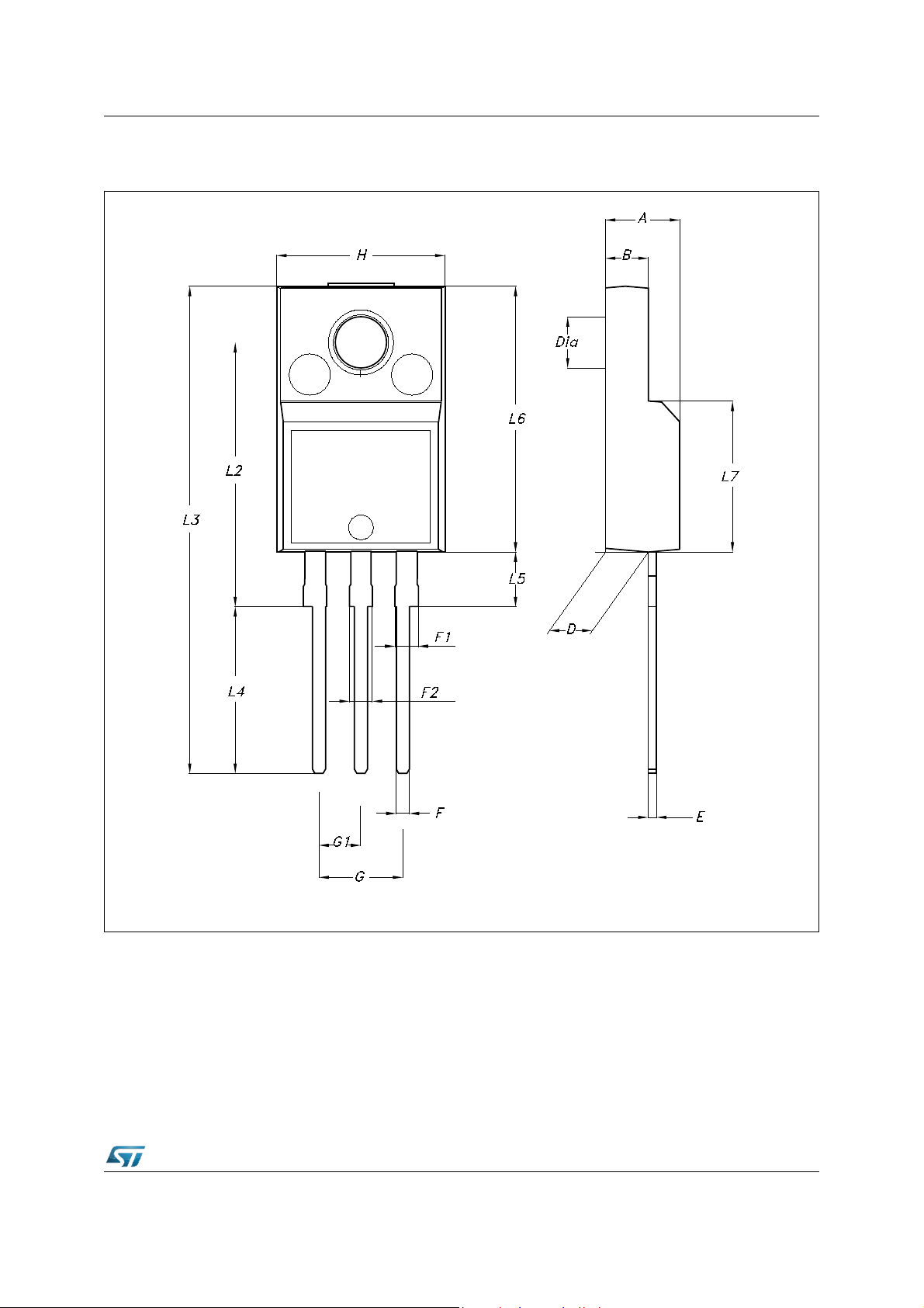
Table 24. TO-220FP mechanical data . . . . . . . . . . . . . . . . . . . . . . . . . . . . . . . . . . . . . . . . . . . . . . . . 44
Table 25. TO-3 mechanical data . . . . . . . . . . . . . . . . . . . . . . . . . . . . . . . . . . . . . . . . . . . . . . . . . . . . 45
Table 26. DPAK mechanical data. . . . . . . . . . . . . . . . . . . . . . . . . . . . . . . . . . . . . . . . . . . . . . . . . . . . 47
Table 27. Tape and reel DPAK mechanical data . . . . . . . . . . . . . . . . . . . . . . . . . . . . . . . . . . . . . . . . 48
Table 28. D²PAK mechanical data . . . . . . . . . . . . . . . . . . . . . . . . . . . . . . . . . . . . . . . . . . . . . . . . . . . 51
Table 29. D²PAK footprint data. . . . . . . . . . . . . . . . . . . . . . . . . . . . . . . . . . . . . . . . . . . . . . . . . . . . . . 52
Table 30. Tape and reel D²PAK mechanical data . . . . . . . . . . . . . . . . . . . . . . . . . . . . . . . . . . . . . . . 53
Table 31. Order codes . . . . . . . . . . . . . . . . . . . . . . . . . . . . . . . . . . . . . . . . . . . . . . . . . . . . . . . . . . . . 54
Table 32. Document revision history . . . . . . . . . . . . . . . . . . . . . . . . . . . . . . . . . . . . . . . . . . . . . . . . . 56
DocID2143 Rev 31 3/57
Page 4

List of figures L78xx, L78xxC, L78xxAB, L78xxAC
List of figures
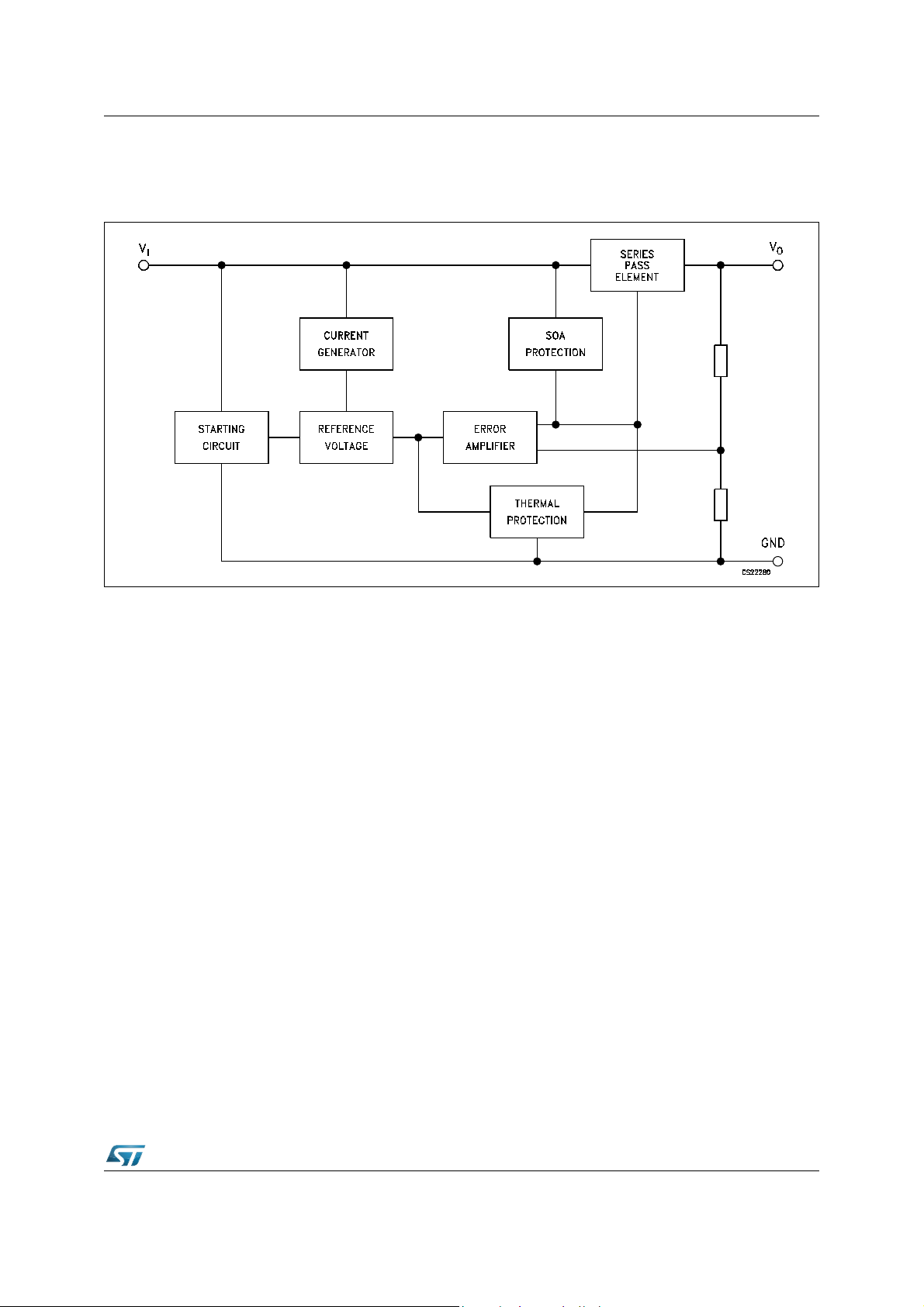
Figure 1. Block diagram. . . . . . . . . . . . . . . . . . . . . . . . . . . . . . . . . . . . . . . . . . . . . . . . . . . . . . . . . . . . 5
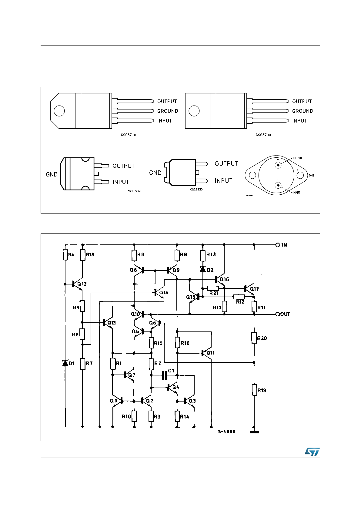
Figure 2. Pin connections (top view) . . . . . . . . . . . . . . . . . . . . . . . . . . . . . . . . . . . . . . . . . . . . . . . . . . 6
Figure 3. Schematic diagram. . . . . . . . . . . . . . . . . . . . . . . . . . . . . . . . . . . . . . . . . . . . . . . . . . . . . . . . 6
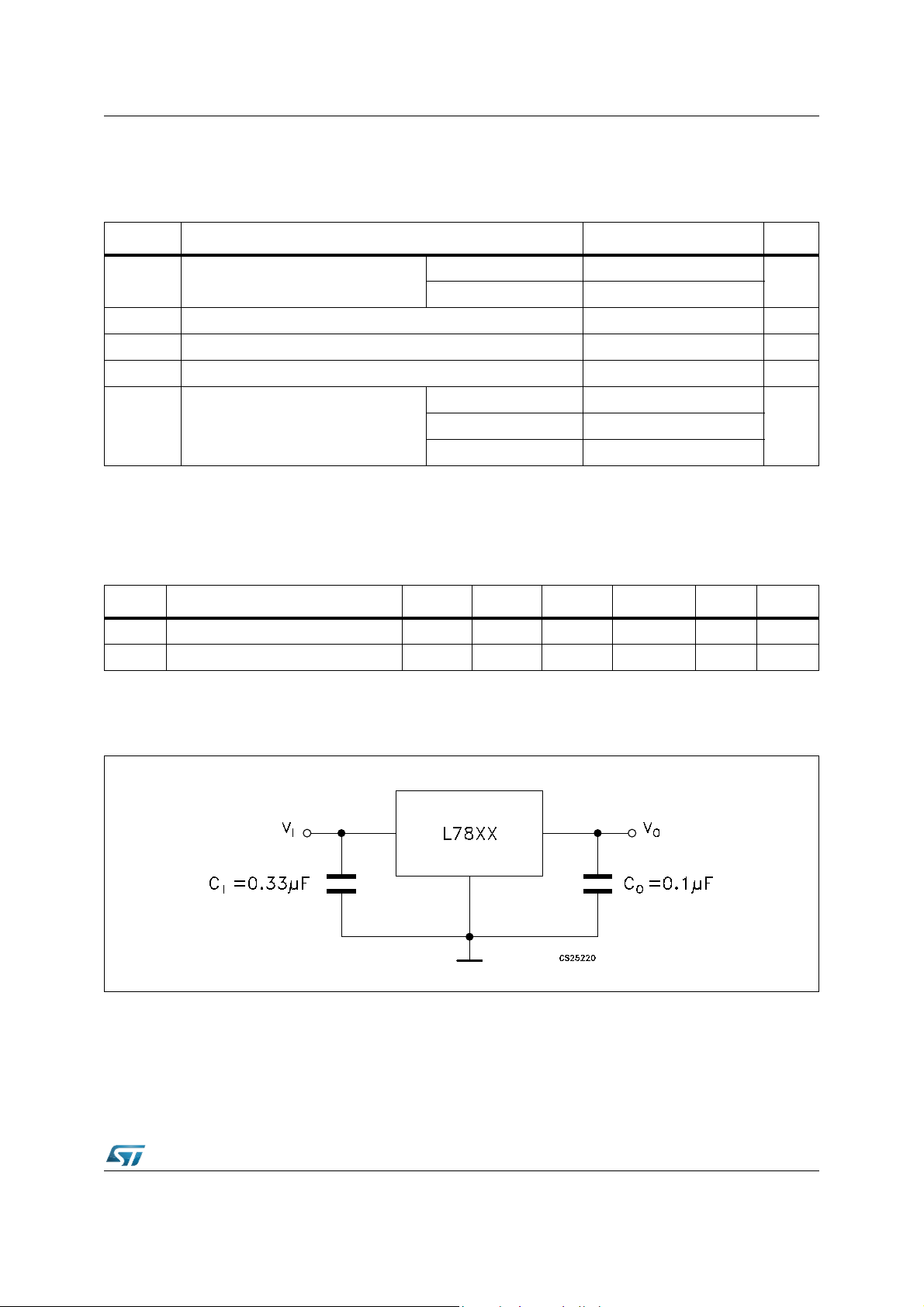
Figure 4. Application circuits . . . . . . . . . . . . . . . . . . . . . . . . . . . . . . . . . . . . . . . . . . . . . . . . . . . . . . . . 7
Figure 5. DC parameter . . . . . . . . . . . . . . . . . . . . . . . . . . . . . . . . . . . . . . . . . . . . . . . . . . . . . . . . . . . . 8
Figure 6. Load regulation. . . . . . . . . . . . . . . . . . . . . . . . . . . . . . . . . . . . . . . . . . . . . . . . . . . . . . . . . . . 8
Figure 7. Ripple rejection. . . . . . . . . . . . . . . . . . . . . . . . . . . . . . . . . . . . . . . . . . . . . . . . . . . . . . . . . . . 8
Figure 8. Fixed output regulator. . . . . . . . . . . . . . . . . . . . . . . . . . . . . . . . . . . . . . . . . . . . . . . . . . . . . 28
Figure 9. Current regulator. . . . . . . . . . . . . . . . . . . . . . . . . . . . . . . . . . . . . . . . . . . . . . . . . . . . . . . . . 29
Figure 10. Circuit for increasing output voltage . . . . . . . . . . . . . . . . . . . . . . . . . . . . . . . . . . . . . . . . . . 29
Figure 11. Adjustable output regulator (7 to 30 V). . . . . . . . . . . . . . . . . . . . . . . . . . . . . . . . . . . . . . . . 29
Figure 12. 0.5 to 10 V regulator . . . . . . . . . . . . . . . . . . . . . . . . . . . . . . . . . . . . . . . . . . . . . . . . . . . . . . 30
Figure 13. High current voltage regulator . . . . . . . . . . . . . . . . . . . . . . . . . . . . . . . . . . . . . . . . . . . . . . 30
Figure 14. High output current with short circuit protection . . . . . . . . . . . . . . . . . . . . . . . . . . . . . . . . . 30
Figure 15. Tracking voltage regulator . . . . . . . . . . . . . . . . . . . . . . . . . . . . . . . . . . . . . . . . . . . . . . . . . 31
Figure 16. Split power supply (± 15 V - 1 A) . . . . . . . . . . . . . . . . . . . . . . . . . . . . . . . . . . . . . . . . . . . . 31
Figure 17. Negative output voltage circuit . . . . . . . . . . . . . . . . . . . . . . . . . . . . . . . . . . . . . . . . . . . . . . 32
Figure 18. Switching regulator . . . . . . . . . . . . . . . . . . . . . . . . . . . . . . . . . . . . . . . . . . . . . . . . . . . . . . . 32
Figure 19. High input voltage circuit (configuration 1) . . . . . . . . . . . . . . . . . . . . . . . . . . . . . . . . . . . . . 32
Figure 20. High input voltage circuit (configuration 2) . . . . . . . . . . . . . . . . . . . . . . . . . . . . . . . . . . . . . 33
Figure 21. High output voltage regulator . . . . . . . . . . . . . . . . . . . . . . . . . . . . . . . . . . . . . . . . . . . . . . . 33
Figure 22. High input and output voltage. . . . . . . . . . . . . . . . . . . . . . . . . . . . . . . . . . . . . . . . . . . . . . . 33
Figure 23. Reducing power dissipation with dropping resistor. . . . . . . . . . . . . . . . . . . . . . . . . . . . . . . 34
Figure 24. Remote shutdown. . . . . . . . . . . . . . . . . . . . . . . . . . . . . . . . . . . . . . . . . . . . . . . . . . . . . . . . 34
Figure 25. Power AM modulator (unity voltage gain, I
Figure 26. Adjustable output voltage with temperature compensation . . . . . . . . . . . . . . . . . . . . . . . . 35
Figure 27. Light controllers (V
Figure 28. Protection against input short-circuit with high capacitance loads . . . . . . . . . . . . . . . . . . . 36
Figure 29. Dropout voltage vs. junction temperature. . . . . . . . . . . . . . . . . . . . . . . . . . . . . . . . . . . . . . 37
Figure 30. Peak output current vs. input/output differential voltage. . . . . . . . . . . . . . . . . . . . . . . . . . . 37
Figure 31. Supply voltage rejection vs. frequency . . . . . . . . . . . . . . . . . . . . . . . . . . . . . . . . . . . . . . . . 37
Figure 32. Output voltage vs. junction temperature. . . . . . . . . . . . . . . . . . . . . . . . . . . . . . . . . . . . . . . 37
Figure 33. Output impedance vs. frequency . . . . . . . . . . . . . . . . . . . . . . . . . . . . . . . . . . . . . . . . . . . . 37
Figure 34. Quiescent current vs. junction temp. . . . . . . . . . . . . . . . . . . . . . . . . . . . . . . . . . . . . . . . . . 37
Figure 35. Load transient response . . . . . . . . . . . . . . . . . . . . . . . . . . . . . . . . . . . . . . . . . . . . . . . . . . . 38
Figure 36. Line transient response . . . . . . . . . . . . . . . . . . . . . . . . . . . . . . . . . . . . . . . . . . . . . . . . . . . 38
Figure 37. Quiescent current vs. input voltage . . . . . . . . . . . . . . . . . . . . . . . . . . . . . . . . . . . . . . . . . . 38
Figure 38. Drawing dimension TO-220 (type STD-ST Dual Gauge) . . . . . . . . . . . . . . . . . . . . . . . . . . 40
Figure 39. Drawing dimension TO-220 (type STD-ST Single Gauge). . . . . . . . . . . . . . . . . . . . . . . . . 41
Figure 40. Drawing dimension tube for TO-220 Dual Gauge (mm.) . . . . . . . . . . . . . . . . . . . . . . . . . . 42
Figure 41. Drawing dimension tube for TO-220 Single Gauge (mm.) . . . . . . . . . . . . . . . . . . . . . . . . . 42
Figure 42. Drawing dimension TO-220FP . . . . . . . . . . . . . . . . . . . . . . . . . . . . . . . . . . . . . . . . . . . . . . 43
Figure 43. Drawing dimension TO-3 . . . . . . . . . . . . . . . . . . . . . . . . . . . . . . . . . . . . . . . . . . . . . . . . . . 45
Figure 44. Drawing dimension DPAK . . . . . . . . . . . . . . . . . . . . . . . . . . . . . . . . . . . . . . . . . . . . . . . . . 46
Figure 45. Drawing dimension tape and reel for DPAK . . . . . . . . . . . . . . . . . . . . . . . . . . . . . . . . . . . . 48
Figure 46. Drawing dimension D²PAK (type STD-ST). . . . . . . . . . . . . . . . . . . . . . . . . . . . . . . . . . . . . 49
Figure 47. Drawing dimension D²PAK (type WOOSEOK-Subcon.). . . . . . . . . . . . . . . . . . . . . . . . . . . 50
Figure 48. D²PAK footprint recommended data. . . . . . . . . . . . . . . . . . . . . . . . . . . . . . . . . . . . . . . . . . 52
Figure 49. Drawing dimension tape and reel for D²PAK . . . . . . . . . . . . . . . . . . . . . . . . . . . . . . . . . . . 53
= VXX + VBE). . . . . . . . . . . . . . . . . . . . . . . . . . . . . . . . . . . . . . . . 35
O(min)
0.5). . . . . . . . . . . . . . . . . . . . . . . . . . . . . . . 34
O
4/57 DocID2143 Rev 31
Page 5
L78xx, L78xxC, L78xxAB, L78xxAC Diagram
1 Diagram
Figure 1. Block diagram
DocID2143 Rev 31 5/57
Page 6
Pin configuration L78xx, L78xxC, L78xxAB, L78xxAC
TO-220FP
TO-3
TO-220
D²PAK (Any Type)
DPAK
2 Pin configuration
Figure 2. Pin connections (top view)
Figure 3. Schematic diagram
6/57 DocID2143 Rev 31
Page 7
L78xx, L78xxC, L78xxAB, L78xxAC Maximum ratings
3 Maximum ratings
Table 2. Absolute maximum ratings
Symbol Parameter Value Unit
for V
= 5 to 18 V 35
O
= 20, 24 V 40
for V
O
for L78xx -55 to 150
for L78xxAB -40 to 125
V
°Cfor L78xxC, L78xxAC 0 to 125
T
P
T
V
I
STG
OP
DC input voltage
I
Output current Internally limited
O
Power dissipation Internally limited
D
Storage temperature range -65 to 150 °C
Operating junction temperature range
Note: Absolute maximum ratings are those values beyond which d amage to the device may occur .
Functional operation under these condition is not implied.
Table 3. Thermal data
Symbol Parameter D²P AK DPAK TO-220 TO-220FP TO-3 Unit
R
R
Thermal resistance junction-case 3 8 5 5 4 °C/W
thJC
Thermal resistance junction-ambient 62.5 100 50 60 35 °C/W
thJA
Figure 4. Application circuits
DocID2143 Rev 31 7/57
Page 8
Test circuits L78xx, L78xxC, L78xxAB, L78xxAC
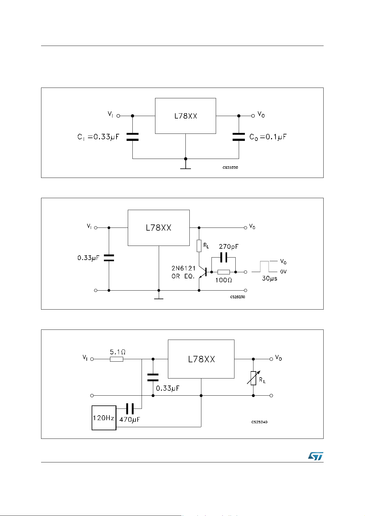
4 Test circuits
Figure 5. DC parameter
Figure 6. Load regulation
Figure 7. Ripple rejection
8/57 DocID2143 Rev 31
Page 9
L78xx, L78xxC, L78xxAB, L78xxAC Electrical characteristics
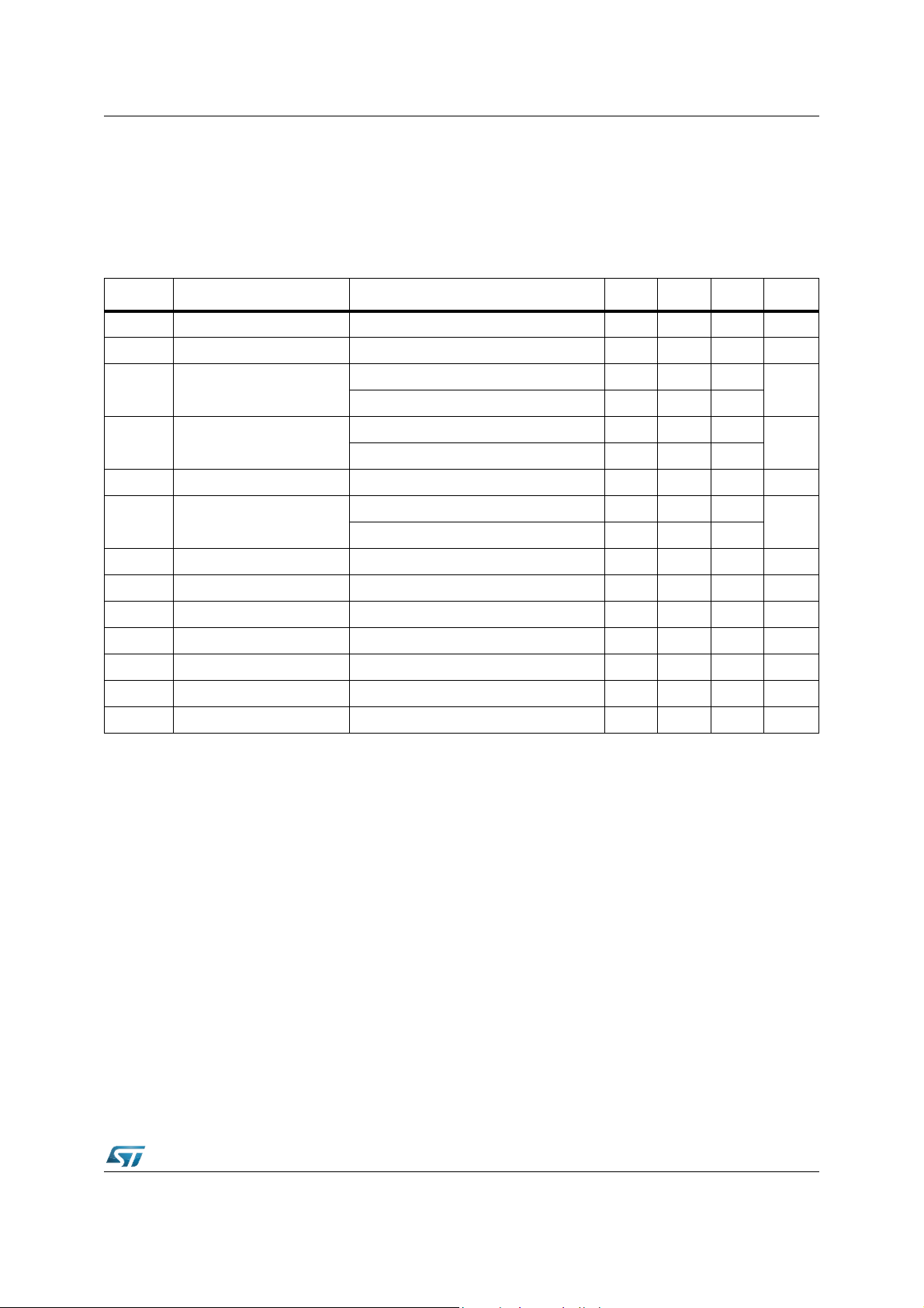
5 Electrical characteristics
Refer to the test circuits , TJ = -55 to 150 °C, VI = 10 V, IO = 500 mA, CI = 0.33 µF,
C
= 0.1 µF unless otherwise specified.
O
Symbol Parameter Test conditions Min. Typ. Max. Unit
Table 4. Electrical characteristics of L7805
V
V
V
V
Output voltage TJ = 25°C 4.8 5 5.2 V
O
Output voltage IO = 5 mA to 1 A, VI = 8 to 20 V 4.65 5 5.35 V
O
(1)
Line regulation
O
(1)
Load regulation
O
Quiescent current TJ = 25°C 6 mA
I
d
VI = 7 to 25 V, TJ = 25°C 3 50
= 8 to 12 V, TJ = 25°C 1 25
V
I
I
= 5 mA to 1.5 A, TJ = 25°C 100
O
= 250 to 750 mA, TJ = 25°C 25
I
O
IO = 5 mA to 1 A 0.5
I
V
eN Output noise voltage B =10 Hz to 100 kHz, T
Quiescent current change
d
/T Output voltage drift IO = 5 mA 0.6 mV/°C
O
= 8 to 25 V 0.8
V
I
= 25°C 40 µV/V
J
SVR Supply voltage rejection VI = 8 to 18 V, f = 120 Hz 68 dB
V
R
I
I
1. Load and line regulation are specified at constant junction temperature. Changes in VO due to heating effects must be
taken into account separately. Pulse testing with low duty cycle is used.
Dropout voltage IO = 1 A, TJ = 25°C 2 2.5 V
d
Output resistance f = 1 kHz 17 m
O
Short circuit current VI = 35 V, TJ = 25°C 0.75 1.2 A
sc
Short circuit peak current TJ = 25°C 1.3 2.2 3.3 A
scp
mV
mV
mA
O
DocID2143 Rev 31 9/57
Page 10
Electrical characteristics L78xx, L78xxC, L78xxAB, L78xxAC
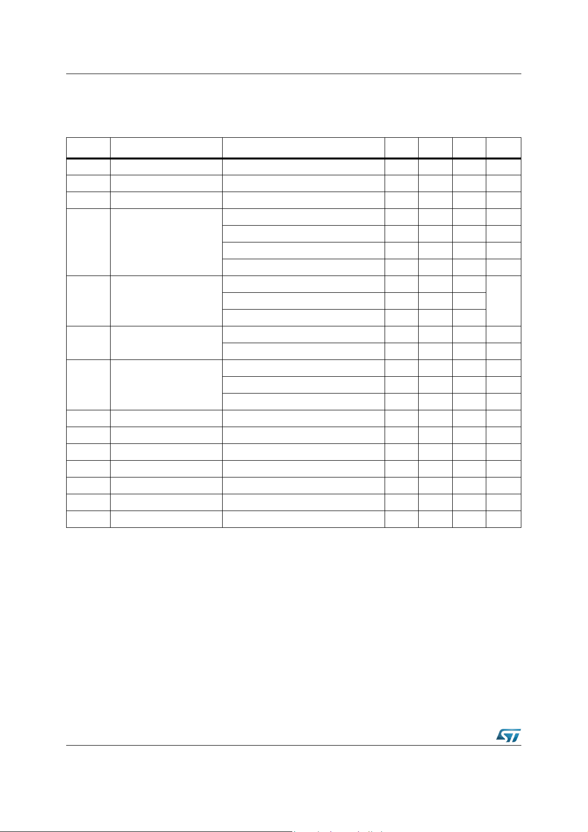
VI = 10 V, IO = 1 A, TJ = 0 to 125 °C (L7805AC), TJ = -40 to 125 °C (L7805AB), unless
otherwise specified.
Symbol Parameter Test conditions Min. Typ. Max. Unit
Table 5. Electrical characteristics of L7805A
V
V
V
V
V
I
SVR Supply voltage rejection V
V
eN Output noise voltage T
R
I
I
V
1. Load and line regulation are specified at constant junction temperature. Changes in VO due to heating effects must be
taken into account separately. Pulse testing with low duty cycle is used.
Output voltage TJ = 25°C 4.9 5 5.1 V
O
Output voltage IO = 5 mA to 1 A, VI = 7.5 to 18 V 4.8 5 5.2 V
O
Output voltage IO = 1 A, VI = 18 to 20 V, TJ = 25°C 4.8 5 5.2 V
O
= 7.5 to 25 V, IO = 500 mA, TJ = 25°C 7 50 mV
V
I
V
= 8 to 12 V 10 50 mV
(1)
Line regulation
O
(1)
Load regulation
O
I
Quiescent current
q
Quiescent current change
q
Dropout voltage IO = 1 A, TJ = 25°C 2 V
d
Output resistance f = 1 kHz 17 m
O
Short circuit current VI = 35 V, TA = 25°C 0.2 A
sc
Short circuit peak current TJ = 25°C 2.2 A
scp
/T Output voltage drift -1.1 mV/°C
O
I
= 8 to 12 V, TJ = 25°C 2 25 mV
V
I
= 7.3 to 20 V, TJ = 25°C 7 50 mV
V
I
I
= 5 mA to 1 A 25 100
O
= 5 mA to 1.5 A, TJ = 25°C 30 100
O
I
= 250 to 750 mA 8 50
O
T
= 25°C 4.3 6 mA
J
6mA
V
= 8 to 23 V, IO = 500 mA 0.8 mA
I
= 7.5 to 20 V, TJ = 25°C 0.8 mA
V
I
= 5 mA to 1 A 0.5 mA
I
O
= 8 to 18 V, f = 120 Hz, IO = 500 mA 68 dB
I
= 25°C, B =10 Hz to 100 kHz 10 µV/V
A
mVI
O
10/57 DocID2143 Rev 31
Page 11
L78xx, L78xxC, L78xxAB, L78xxAC Electrical characteristics
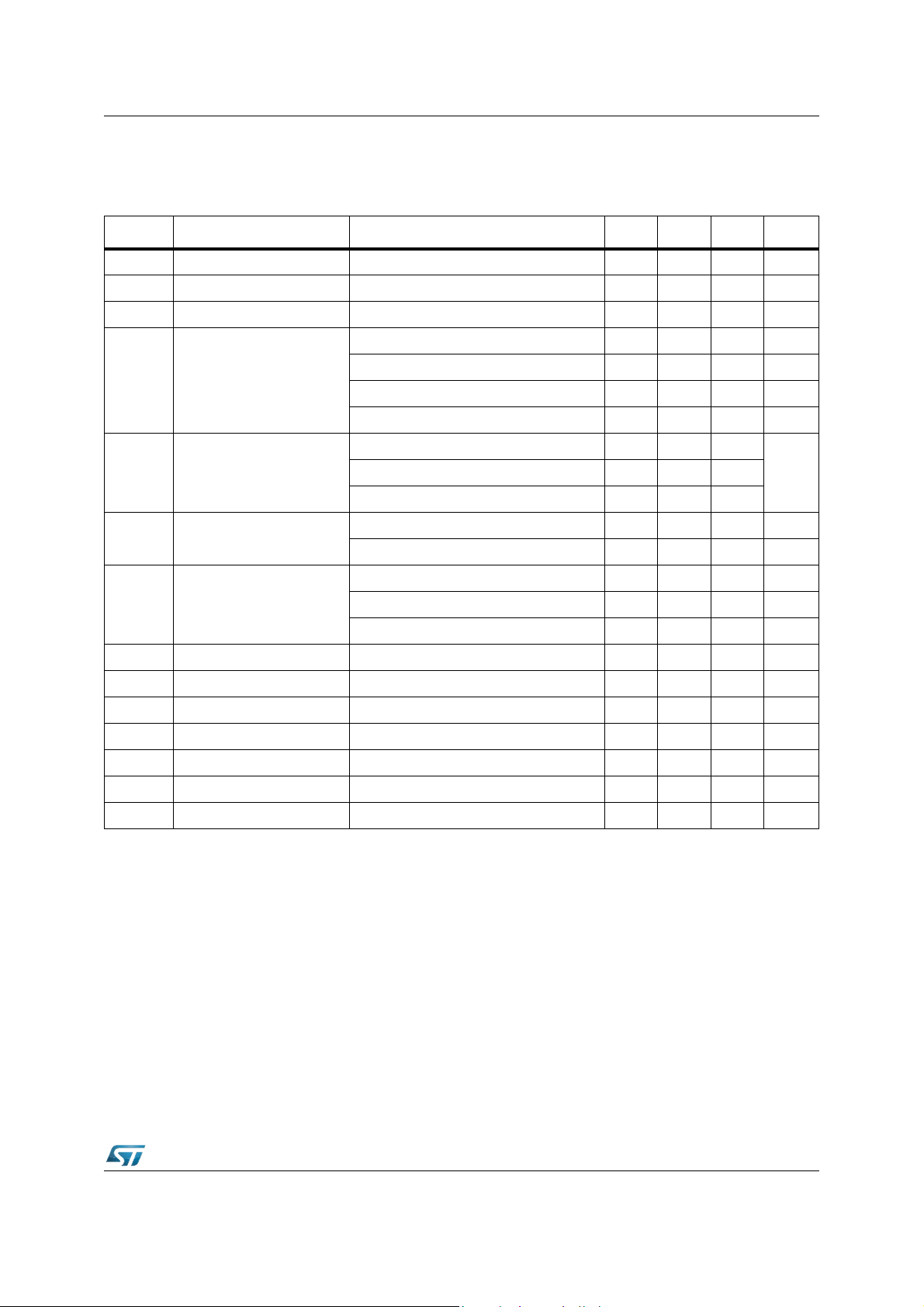
VI = 11 V, IO = 1 A, TJ = 0 to 125 °C (L7806AC), TJ = -40 to 125 °C (L7806AB), unless
otherwise specified.
Symbol Parameter Test conditions Min. Typ. Max. Unit
Table 6. Electrical characteristics of L7806A
V
V
V
V
V
I
SVR Supply voltage rejection V
V
eN Output noise voltage T
R
I
I
V
1. Load and line regulation are specified at constant junction temperature. Changes in VO due to heating effects must be
taken into account separately. Pulse testing with low duty cycle is used.
Output voltage TJ = 25°C 5.88 6 6.12 V
O
Output voltage IO = 5 mA to 1 A, VI = 8.6 to 19 V 5.76 6 6.24 V
O
Output voltage IO = 1 A, VI = 19 to 21 V, TJ = 25°C 5.76 6 6.24 V
O
= 8.6 to 25 V, IO = 500 mA, TJ = 25°C 9 60 mV
V
I
V
= 9 to 13 V 11 60 mV
(1)
Line regulation
O
(1)
Load regulation
O
I
Quiescent current
q
Quiescent current change
q
Dropout voltage IO = 1 A, TJ = 25°C 2 V
d
Output resistance f = 1 kHz 17 m
O
Short circuit current VI = 35 V, TA = 25°C 0.2 A
sc
Short circuit peak current TJ = 25°C 2.2 A
scp
/T Output voltage drift -0.8 mV/°C
O
I
= 9 to 13 V, TJ = 25°C 3 30 mV
V
I
= 8.3 to 21 V, TJ = 25°C 9 60 mV
V
I
I
= 5 mA to 1 A 25 100
O
= 5 mA to 1.5 A, TJ = 25°C 30 100
O
I
= 250 to 750 mA 10 50
O
T
= 25°C 4.3 6 mA
J
6mA
V
= 9 to 24 V, IO = 500 mA 0.8 mA
I
= 8.6 to 21 V, TJ = 25°C 0.8 mA
V
I
= 5 mA to 1 A 0.5 mA
I
O
= 9 to 19 V, f = 120 Hz, IO = 500 mA 65 dB
I
= 25°C, B =10 Hz to 100 kHz 10 µV/V
A
mVI
O
DocID2143 Rev 31 1 1/57
Page 12
Electrical characteristics L78xx, L78xxC, L78xxAB, L78xxAC
VI = 14 V, IO = 1 A, TJ = 0 to 125 °C (L7808AC), TJ = -40 to 125 °C (L7808AB), unless
otherwise specified.
Symbol Parameter Test conditions Min. Typ. Max. Unit
Table 7. Electrical characteristics of L7808A
V
V
V
V
V
I
Output voltage TJ = 25°C 7.84 8 8.16 V
O
Output voltage IO = 5 mA to 1 A, VI = 10.6 to 21 V 7.7 8 8.3 V
O
Output voltage IO = 1 A, VI = 21 to 23 V, TJ = 25°C 7.7 8 8.3 V
O
(1)
Line regulation
O
(1)
Load regulation
O
I
Quiescent current
q
Quiescent current change
q
SVR Supply voltage rejection
V
= 10.6 to 25 V, IO = 500 mA,
I
= 25°C
T
J
= 11 to 17 V 15 80 mV
V
I
= 11 to 17 V, TJ = 25°C 5 40 mV
V
I
V
= 10.4 to 23 V, TJ = 25°C 12 80 mV
I
= 5 mA to 1 A 25 100
I
O
= 5 mA to 1.5 A, TJ = 25°C 30 100
O
= 250 to 750 mA 10 50
I
O
T
= 25°C 4.3 6 mA
J
12 80 mV
6mA
V
= 11 to 23 V, IO = 500 mA 0.8 mA
I
= 10.6 to 23 V, TJ = 25°C 0.8 mA
V
I
I
= 5 mA to 1 A 0.5 mA
O
= 11.5 to 21.5 V, f = 120 Hz,
V
I
IO = 500 mA
62 dB
mVI
V
eN Output noise voltage T
R
I
I
V
1. Load and line regulation are specified at constant junction temperature. Changes in VO due to heating effects must be
taken into account separately. Pulse testing with low duty cycle is used.
Dropout voltage IO = 1 A, TJ = 25°C 2 V
d
= 25°C, B =10 Hz to 100 kHz 10 µV/V
A
Output resistance f = 1 kHz 18 m
O
Short circuit current VI = 35 V, TA = 25°C 0.2 A
sc
Short circuit peak current TJ = 25°C 2.2 A
scp
/T Output voltage drift -0.8 mV/°C
O
12/57 DocID2143 Rev 31
O
Page 13
L78xx, L78xxC, L78xxAB, L78xxAC Electrical characteristics
VI = 15 V, IO = 1 A, TJ = 0 to 125 °C (L7809AC), TJ = -40 to 125 °C (L7809AB), unless
otherwise specified.
Symbol Parameter Test conditions Min. Typ. Max. Unit
Table 8. Electrical characteristics of L7809A
V
V
V
V
V
I
Output voltage TJ = 25°C 8.82 9 9.18 V
O
Output voltage IO = 5 mA to 1 A, VI = 10.6 to 22 V 8.65 9 9.35 V
O
Output voltage IO = 1 A, VI = 22 to 24 V, TJ = 25°C 8.65 9 9.35 V
O
(1)
Line regulation
O
(1)
Load regulation
O
I
Quiescent current
q
Quiescent current change
q
SVR Supply voltage rejection
V
= 10.6 to 25 V, IO = 500 mA,
I
= 25°C
T
J
= 11 to 17 V 15 90 mV
V
I
= 11 to 17 V, TJ = 25°C 5 45 mV
V
I
V
= 11.4 to 23 V, TJ = 25°C 12 90 mV
I
= 5 mA to 1 A 25 100
I
O
= 5 mA to 1.5 A, TJ = 25°C 30 100
O
= 250 to 750 mA 10 50
I
O
T
= 25°C 4.3 6 mA
J
12 90 mV
6mA
V
= 11 to 25 V, IO = 500 mA 0.8 mA
I
= 10.6 to 23 V, TJ = 25°C 0.8 mA
V
I
I
= 5 mA to 1 A 0.5 mA
O
= 11.5 to 21.5 V, f = 120 Hz,
V
I
IO = 500 mA
61 dB
mVI
V
eN Output noise voltage T
R
I
I
V
1. Load and line regulation are specified at constant junction temperature. Changes in VO due to heating effects must be
taken into account separately. Pulse testing with low duty cycle is used.
Dropout voltage IO = 1 A, TJ = 25°C 2 V
d
= 25°C, B =10 Hz to 100 kHz 10 µV/V
A
Output resistance f = 1 kHz 18 m
O
Short circuit current VI = 35 V, TA = 25°C 0.2 A
sc
Short circuit peak current TJ = 25°C 2.2 A
scp
/T Output voltage drift -0.8 mV/°C
O
DocID2143 Rev 31 13/57
O
Page 14
Electrical characteristics L78xx, L78xxC, L78xxAB, L78xxAC
VI = 19 V, IO = 1 A, TJ = 0 to 125 °C (L7812AC), TJ = -40 to 125 °C (L7812AB), unless
otherwise specified.
Symbol Parameter Test conditions Min. Typ. Max. Unit
Table 9. Electrical characteristics of L7812A
V
V
V
V
V
I
SVR Supply voltage rejection V
V
eN Output noise voltage T
R
I
I
V
1. Load and line regulation are specified at constant junction temperature. Changes in VO due to heating effects must be
taken into account separately. Pulse testing with low duty cycle is used.
Output voltage TJ = 25°C 11.75 12 12.25 V
O
Output voltage IO = 5 mA to 1 A, VI = 14.8 to 25 V 11.5 12 12.5 V
O
Output voltage IO = 1 A, VI = 25 to 27 V, TJ = 25°C 11.5 12 12.5 V
O
V
= 14.8 to 30 V, IO = 500 mA,
I
= 25°C
T
J
(1)
Line regulation
O
(1)
Load regulation
O
I
Quiescent current
q
Quiescent current change
q
Dropout voltage IO = 1 A, TJ = 25°C 2 V
d
Output resistance f = 1 kHz 18 m
O
Short circuit current VI = 35 V, TA = 25°C 0.2 A
sc
Short circuit peak current TJ = 25°C 2.2 A
scp
/T Output voltage drift -1 mV/°C
O
= 16 to 12 V 16 120 mV
V
I
= 16 to 12 V, TJ = 25°C 6 60 mV
V
I
V
= 14.5 to 27 V, TJ = 25°C 13 120 mV
I
= 5 mA to 1 A 25 100
I
O
= 5 mA to 1.5 A, TJ = 25°C 30 100
O
= 250 to 750 mA 10 50
I
O
T
= 25°C 4.4 6 mA
J
V
= 15 to 30 V, IO = 500 mA 0.8 mA
I
= 14.8 to 27 V, TJ = 25°C 0.8 mA
V
I
I
= 5 mA to 1 A 0.5 mA
O
= 15 to 25 V, f = 120 Hz, IO = 500 mA 60 dB
I
= 25°C, B = 10 Hz to 100 kHz 10 µV/V
A
13 120 mV
6mA
mVI
O
14/57 DocID2143 Rev 31
Page 15
L78xx, L78xxC, L78xxAB, L78xxAC Electrical characteristics
VI = 23 V, IO = 1 A, TJ = 0 to 125 °C (L7815AC), TJ = -40 to 125 °C (L7815AB), unless
otherwise specified.
Symbol Parameter Test conditions Min. Typ. Max. Unit
Table 10. Electrical characteristics of L7815A
V
V
V
V
V
I
Output voltage TJ = 25°C 14.7 15 15.3 V
O
Output voltage IO = 5 mA to 1 A, VI = 17.9 to 28 V 14.4 15 15.6 V
O
Output voltage IO = 1 A, VI = 28 to 30 V, TJ = 25°C 14.4 15 15.6 V
O
(1)
Line regulation
O
(1)
Load regulation
O
I
Quiescent current
q
Quiescent current change
q
SVR Supply voltage rejection
V
= 17.9 to 30 V, IO = 500 mA,
I
= 25°C
T
J
= 20 to 26 V 16 150 mV
V
I
= 20 to 26 V, TJ = 25°C 6 75 mV
V
I
V
= 17.5 to 30 V, TJ = 25°C 13 150 mV
I
= 5 mA to 1 A 25 100
I
O
= 5 mA to 1.5 A, TJ = 25°C 30 100
O
= 250 to 750 mA 10 50
I
O
T
= 25°C 4.4 6 mA
J
13 150 mV
6mA
V
= 17.5 to 30 V, IO = 500 mA 0.8 mA
I
= 17.5 to 30 V, TJ = 25°C 0.8 mA
V
I
I
= 5 mA to 1 A 0.5 mA
O
= 18.5 to 28.5 V, f = 120 Hz,
V
I
IO = 500 mA
58 dB
mVI
V
eN Output noise voltage T
R
I
I
V
1. Load and line regulation are specified at constant junction temperature. Changes in VO due to heating effects must be
taken into account separately. Pulse testing with low duty cycle is used.
Dropout voltage IO = 1 A, TJ = 25°C 2 V
d
= 25°C, B = 10Hz to 100 kHz 10 µV/V
A
Output resistance f = 1 kHz 19 m
O
Short circuit current VI = 35 V, TA = 25°C 0.2 A
sc
Short circuit peak current TJ = 25°C 2.2 A
scp
/T Output voltage drift -1 mV/°C
O
DocID2143 Rev 31 15/57
O
Page 16
Electrical characteristics L78xx, L78xxC, L78xxAB, L78xxAC
VI = 33 V, IO = 1 A, TJ = 0 to 125 °C (L7824AC), TJ = -40 to 125 °C (L7824AB), unless
otherwise specified.
Symbol Parameter Test conditions Min. Typ. Max. Unit
Table 11. Electrical characteristics of L7824A
V
V
V
V
V
I
SVR Supply voltage rejection V
V
eN Output noise voltage T
R
I
I
V
1. Load and line regulation are specified at constant junction temperature. Changes in VO due to heating effects must be
taken into account separately. Pulse testing with low duty cycle is used.
Output voltage TJ = 25°C 23.5 24 24.5 V
O
Output voltage IO = 5 mA to 1 A, VI = 27.3 to 37 V 23 24 25 V
O
Output voltage IO = 1 A, VI = 37 to 38 V, TJ = 25°C 23 24 25 V
O
= 27 to 38 V, IO = 500 mA, TJ = 25°C 31 240 mV
V
I
V
= 30 to 36 V 35 200 mV
(1)
Line regulation
O
(1)
Load regulation
O
I
Quiescent current
q
Quiescent current change
q
Dropout voltage IO = 1 A, TJ = 25°C 2 V
d
Output resistance f = 1 kHz 20 m
O
Short circuit current VI = 35 V, TA = 25°C 0.2 A
sc
Short circuit peak current TJ = 25°C 2.2 A
scp
/T Output voltage drift -1.5 mV/°C
O
I
= 30 to 36 V, TJ = 25°C 14 120 mV
V
I
= 26.7 to 38 V, TJ = 25°C 31 240 mV
V
I
I
= 5 mA to 1 A 25 100
O
= 5 mA to 1.5 A, TJ = 25°C 30 100
O
I
= 250 to 750 mA 10 50
O
T
= 25°C 4.6 6 mA
J
6mA
V
= 27.3 to 38 V, IO = 500 mA 0.8 mA
I
= 27.3 to 38 V, TJ = 25°C 0.8 mA
V
I
= 5 mA to 1 A 0.5 mA
I
O
= 28 to 38 V, f = 120 Hz, IO = 500 mA 54 dB
I
= 25°C, B = 10 Hz to 100 kHz 10 µV/V
A
mVI
O
16/57 DocID2143 Rev 31
Page 17
L78xx, L78xxC, L78xxAB, L78xxAC Electrical characteristics
Refer to the test circuits, TJ = 0 to 125 °C, VI = 10 V, IO = 500 mA, CI = 0.33 µF, CO = 0.1 µF
unless otherwise specified.
Symbol Parameter Test conditions Min. Typ. Max. Unit
Table 12. Electrical characteristics of L7805C
V
V
V
V
V
I
V
eN Output noise voltage B = 10 Hz to 100 kHz, T
Output voltage TJ = 25°C 4.8 5 5.2 V
O
Output voltage IO = 5 mA to 1 A, VI = 7 to 18 V 4.75 5 5.25 V
O
Output voltage IO = 1 A, VI = 18 to 20V, TJ = 25°C 4.75 5 5.25 V
O
V
= 7 to 25 V, TJ = 25°C 3 100
(1)
Line regulation
O
(1)
Load regulation
O
I
Quiescent current TJ = 25°C 8 mA
d
Quiescent current change
d
/T Output voltage drift IO = 5 mA -1.1 mV/°C
O
I
= 8 to 12 V, TJ = 25°C 1 50
V
I
I
= 5 mA to 1.5 A, TJ = 25°C 100
O
= 250 to 750 mA, TJ = 25°C 50
I
O
I
= 5 mA to 1 A 0.5
O
= 7 to 23 V 0.8
V
I
= 25°C 40 µV/V
J
SVR Supply voltage rejection VI = 8 to 18 V, f = 120 Hz 62 dB
V
R
I
I
1. Load and line regulation are specified at constant junction temperature. Changes in VO due to heating effects must be
taken into account separately. Pulse testing with low duty cycle is used.
Dropout voltage IO = 1 A, TJ = 25°C 2 V
d
Output resistance f = 1 kHz 17 m
O
Short circuit current VI = 35 V, TJ = 25°C 0.75 A
sc
Short circuit peak current TJ = 25°C 2.2 A
scp
mV
mV
mA
O
DocID2143 Rev 31 17/57
Page 18
Electrical characteristics L78xx, L78xxC, L78xxAB, L78xxAC
Refer to the test circuits, TJ = 0 to 125 °C, VI = 1 1 V, IO = 500 mA, CI = 0.33 µF, CO = 0.1 µF
unless otherwise specified.
Symbol Parameter Test conditions Min. Typ. Max. Unit
Table 13. Electrical characteristics of L7806C
V
V
V
V
V
I
V
eN Output noise voltage B = 10 Hz to 100 kHz, T
Output voltage TJ = 25°C 5.75 6 6.25 V
O
Output voltage IO = 5 mA to 1 A, VI = 8 to 19 V 5.7 6 6.3 V
O
Output voltage IO = 1 A, VI = 19 to 21 V, TJ = 25°C 5.7 6 6.3 V
O
V
= 8 to 25 V, TJ = 25°C 120
(1)
Line regulation
O
(1)
Load regulation
O
I
Quiescent current TJ = 25°C 8 mA
d
Quiescent current change
d
/T Output voltage drift IO = 5 mA -0.8 mV/°C
O
I
= 9 to 13 V, TJ = 25°C 60
V
I
I
= 5 mA to 1.5 A, TJ = 25°C 120
O
= 250 to 750 mA, TJ = 25°C 60
I
O
I
= 5 mA to 1 A 0.5
O
= 8 to 24 V 1.3
V
I
= 25°C 45 µV/V
J
SVR Supply voltage rejection VI = 9 to 19 V, f = 120 Hz 59 dB
V
R
I
I
1. Load and line regulation are specified at constant junction temperature. Changes in VO due to heating effects must be
taken into account separately. Pulse testing with low duty cycle is used.
Dropout voltage IO = 1 A, TJ = 25°C 2 V
d
Output resistance f = 1 kHz 19 m
O
Short circuit current VI = 35 V, TJ = 25°C 0.55 A
sc
Short circuit peak current TJ = 25°C 2.2 A
scp
mV
mV
mA
O
18/57 DocID2143 Rev 31
Page 19
L78xx, L78xxC, L78xxAB, L78xxAC Electrical characteristics
Refer to the test circuits, TJ = 0 to 125 °C, VI = 14 V, IO = 500 mA, CI = 0.33 µF, CO = 0.1 µF
unless otherwise specified.
Symbol Parameter Test conditions Min. Typ. Max. Unit
Table 14. Electrical characteristics of L7808C
V
V
V
V
V
I
V
eN Output noise voltage B = 10 Hz to 100 kHz, T
Output voltage TJ = 25°C 7.7 8 8.3 V
O
Output voltage IO = 5 mA to 1 A, VI = 10.5 to 21 V 7.6 8 8.4 V
O
Output voltage IO = 1 A, VI = 21 to 25 V, TJ = 25°C 7.6 8 8.4 V
O
V
= 10.5 to 25 V, TJ = 25°C 160
(1)
Line regulation
O
(1)
Load regulation
O
I
Quiescent current TJ = 25°C 8 mA
d
Quiescent current change
d
/T Output voltage drift IO = 5 mA -0.8 mV/°C
O
I
= 11 to 17 V, TJ = 25°C 80
V
I
I
= 5 mA to 1.5 A, TJ = 25°C 160
O
= 250 to 750 mA, TJ = 25°C 80
I
O
I
= 5 mA to 1 A 0.5
O
= 10.5 to 25 V 1
V
I
= 25°C 52 µV/V
J
SVR Supply voltage rejection VI = 11.5 to 21.5 V, f = 120 Hz 56 dB
V
R
I
I
1. Load and line regulation are specified at constant junction temperature. Changes in VO due to heating effects must be
taken into account separately. Pulse testing with low duty cycle is used.
Dropout voltage IO = 1 A, TJ = 25°C 2 V
d
Output resistance f = 1 kHz 16 m
O
Short circuit current VI = 35 V, TJ = 25°C 0.45 A
sc
Short circuit peak current TJ = 25°C 2.2 A
scp
mV
mV
mA
O
DocID2143 Rev 31 19/57
Page 20
Electrical characteristics L78xx, L78xxC, L78xxAB, L78xxAC
Refer to the test circuits , TJ = 0 to 125 °C, VI = 14.5 V, IO = 500 mA, CI = 0.33 µF,
C
= 0.1 µF unless otherwise specified.
O
Symbol Parameter Test conditions Min. Typ. Max. Unit
Table 15. Electrical characteristics of L7885C
V
V
V
V
V
I
V
eN Output noise voltage B = 10 Hz to 100 kHz, T
Output voltage TJ = 25°C 8.2 8.5 8.8 V
O
Output voltage IO = 5 mA to 1 A, VI = 11 to 21.5 V 8.1 8.5 8.9 V
O
Output voltage IO = 1 A, VI = 21.5 to 26 V, TJ = 25°C 8.1 8.5 8.9 V
O
V
= 11 to 27 V, TJ = 25°C 160
(1)
Line regulation
O
(1)
Load regulation
O
I
Quiescent current TJ = 25°C 8 mA
d
Quiescent current change
d
/T Output voltage drift IO = 5 mA -0.8 mV/°C
O
I
= 11.5 to 17.5 V, TJ = 25°C 80
V
I
I
= 5 mA to 1.5 A, TJ = 25°C 160
O
= 250 to 750 mA, TJ = 25°C 80
I
O
I
= 5 mA to 1 A 0.5
O
= 11 to 26 V 1
V
I
= 25°C 55 µV/V
J
SVR Supply voltage rejection VI = 12 to 22 V, f = 120 Hz 56 dB
V
R
I
I
1. Load and line regulation are specified at constant junction temperature. Changes in VO due to heating effects must be
taken into account separately. Pulse testing with low duty cycle is used.
Dropout voltage IO = 1 A, TJ = 25°C 2 V
d
Output resistance f = 1 kHz 16 m
O
Short circuit current VI = 35 V, TJ = 25°C 0.45 A
sc
Short circuit peak current TJ = 25°C 2.2 A
scp
mV
mV
mA
O
20/57 DocID2143 Rev 31
Page 21
L78xx, L78xxC, L78xxAB, L78xxAC Electrical characteristics
Refer to the test circuits, TJ = 0 to 125 °C, VI = 15 V, IO = 500 mA, CI = 0.33 µF, CO = 0.1 µF
unless otherwise specified.
Symbol Parameter Test conditions Min. Typ. Max. Unit
Table 16. Electrical characteristics of L7809C
V
V
V
V
V
I
V
eN Output noise voltage B = 10 Hz to 100 kHz, T
Output voltage TJ = 25°C 8.64 9 9.36 V
O
Output voltage IO = 5 mA to 1 A, VI = 11.5 to 22 V 8.55 9 9.45 V
O
Output voltage IO = 1 A, VI = 22 to 26 V, TJ = 25°C 8.55 9 9.45 V
O
V
= 11.5 to 26 V, TJ = 25°C 180
(1)
Line regulation
O
(1)
Load regulation
O
I
Quiescent current TJ = 25°C 8 mA
d
Quiescent current change
d
/T Output voltage drift IO = 5 mA -1 mV/°C
O
I
= 12 to 18 V, TJ = 25°C 9 0
V
I
I
= 5 mA to 1.5 A, TJ = 25°C 180
O
= 250 to 750 mA, TJ = 25°C 90
I
O
I
= 5 mA to 1 A 0.5
O
= 11.5 to 26 V 1
V
I
= 25°C 70 µV/V
J
SVR Supply voltage rejection VI = 12 to 23 V, f = 120 Hz 55 dB
V
R
I
I
1. Load and line regulation are specified at constant junction temperature. Changes in VO due to heating effects must be
taken into account separately. Pulse testing with low duty cycle is used.
Dropout voltage IO = 1 A, TJ = 25°C 2 V
d
Output resistance f = 1 kHz 17 m
O
Short circuit current VI = 35 V, TJ = 25°C 0.40 A
sc
Short circuit peak current TJ = 25°C 2.2 A
scp
mV
mV
mA
O
DocID2143 Rev 31 21/57
Page 22
Electrical characteristics L78xx, L78xxC, L78xxAB, L78xxAC
Refer to the test circuits, TJ = 0 to 125 °C, VI = 15 V, IO = 500 mA, CI = 0.33 µF, CO = 0.1 µF
unless otherwise specified.
Symbol Parameter Test conditions Min. Typ. Max. Unit
Table 17. Electrical characteristics of L7810C
V
V
V
V
V
I
V
eN Output noise voltage B = 10 Hz to 100 kHz, T
Output voltage TJ = 25°C 9.6 10 10.4 V
O
Output voltage IO = 5 mA to 1 A, VI = 12.5 to 23 V 9.5 10 10.5 V
O
Output voltage IO = 1 A, VI = 23 to 26 V, TJ = 25°C 9.5 10 10.5 V
O
V
= 12.5 to 26 V, TJ = 25°C 200
(1)
Line regulation
O
(1)
Load regulation
O
I
Quiescent current TJ = 25°C 8 mA
d
Quiescent current change
d
/T Output voltage drift IO = 5 mA -1 mV/°C
O
I
= 13.5 to 19 V, TJ = 25°C 100
V
I
I
= 5 mA to 1.5 A, TJ = 25°C 200
O
= 250 to 750 mA, TJ = 25°C 100
I
O
I
= 5 mA to 1 A 0.5
O
= 12.5 to 26 V 1
V
I
= 25°C 70 µV/V
J
SVR Supply voltage rejection VI = 13 to 23 V, f = 120 Hz 55 dB
V
R
I
I
1. Load and line regulation are specified at constant junction temperature. Changes in VO due to heating effects must be
taken into account separately. Pulse testing with low duty cycle is used.
Dropout voltage IO = 1 A, TJ = 25°C 2 V
d
Output resistance f = 1 kHz 17 m
O
Short circuit current VI = 35 V, TJ = 25°C 0.40 A
sc
Short circuit peak current TJ = 25°C 2.2 A
scp
mV
mV
mA
O
22/57 DocID2143 Rev 31
Page 23
L78xx, L78xxC, L78xxAB, L78xxAC Electrical characteristics
Refer to the test circuits, TJ = 0 to 125 °C, VI = 19 V, IO = 500 mA, CI = 0.33 µF, CO = 0.1 µF
unless otherwise specified.
Symbol Parameter Test conditions Min. Typ. Max. Unit
Table 18. Electrical characteristics of L7812C
V
V
V
V
V
I
V
eN Output noise voltage B = 10 Hz to 100 kHz, T
Output voltage TJ = 25°C 11.5 12 12.5 V
O
Output voltage IO = 5 mA to 1 A, VI = 14.5 to 25 V 11.4 12 12.6 V
O
Output voltage IO = 1 A, VI = 25 to 27 V, TJ = 25°C 11.4 12 12.6 V
O
V
= 14.5 to 30 V, TJ = 25°C 240
(1)
Line regulation
O
(1)
Load regulation
O
I
Quiescent current TJ = 25°C 8 mA
d
Quiescent current change
d
/T Output voltage drift IO = 5 mA -1 mV/°C
O
I
= 16 to 22 V, TJ = 25°C 120
V
I
I
= 5 mA to 1.5 A, TJ = 25°C 240
O
= 250 to 750 mA, TJ = 25°C 120
I
O
I
= 5 mA to 1 A 0.5
O
= 14.5 to 30 V 1
V
I
= 25°C 75 µV/V
J
SVR Supply voltage rejection VI = 15 to 25 V, f = 120 Hz 55 dB
V
R
I
I
1. Load and line regulation are specified at constant junction temperature. Changes in VO due to heating effects must be
taken into account separately. Pulse testing with low duty cycle is used.
Dropout voltage IO = 1 A, TJ = 25°C 2 V
d
Output resistance f = 1 kHz 18 m
O
Short circuit current VI = 35 V, TJ = 25°C 0.35 A
sc
Short circuit peak current TJ = 25°C 2.2 A
scp
mV
mV
mA
O
DocID2143 Rev 31 23/57
Page 24
Electrical characteristics L78xx, L78xxC, L78xxAB, L78xxAC
Refer to the test circuits, TJ = 0 to 125 °C, VI = 23 V, IO = 500 mA, CI = 0.33 µF, CO = 0.1 µF
unless otherwise specified.
Symbol Parameter Test conditions Min. Typ. Max. Unit
Table 19. Electrical characteristics of L7815C
V
V
V
V
V
I
V
eN Output noise voltage B = 10 Hz to 100kHz, T
Output voltage TJ = 25°C 14.4 15 15.6 V
O
Output voltage IO = 5 mA to 1 A, VI = 17.5 to 28 V 14.25 15 15.75 V
O
Output voltage IO = 1 A, VI = 28 to 30 V, TJ = 25°C 14.25 15 15.75 V
O
V
= 17.5 to 30 V, TJ = 25°C 300
(1)
Line regulation
O
(1)
Load regulation
O
I
Quiescent current TJ = 25°C 8 mA
d
Quiescent current change
d
/T Output voltage drift IO = 5 mA -1 mV/°C
O
I
= 20 to 26 V, TJ = 25°C 150
V
I
I
= 5 mA to 1.5 A, TJ = 25°C 300
O
= 250 to 750 mA, TJ = 25°C 150
I
O
I
= 5 mA to 1A 0.5
O
= 17.5 to 30 V 1
V
I
= 25°C 90 µV/V
J
SVR Supply voltage rejection VI = 18.5 to 28.5 V, f = 120 Hz 54 dB
V
R
I
I
1. Load and line regulation are specified at constant junction temperature. Changes in VO due to heating effects must be
taken into account separately. Pulse testing with low duty cycle is used.
Dropout voltage IO = 1 A, TJ = 25°C 2 V
d
Output resistance f = 1 kHz 19 m
O
Short circuit current VI = 35 V, TJ = 25°C 0.23 A
sc
Short circuit peak current TJ = 25°C 2.2 A
scp
mV
mV
mA
O
24/57 DocID2143 Rev 31
Page 25
L78xx, L78xxC, L78xxAB, L78xxAC Electrical characteristics
Refer to the test circuits, TJ = 0 to 125 °C, VI = 26 V, IO = 500 mA, CI = 0.33 µF, CO = 0.1 µF
unless otherwise specified.
Symbol Parameter Test conditions Min. Typ. Max. Unit
Table 20. Electrical characteristics of L7818C
V
V
V
V
V
I
V
eN Output noise voltage B = 10 Hz to 100 kHz, T
Output voltage TJ = 25°C 17.3 18 18.7 V
O
Output voltage IO = 5 mA to 1 A, VI = 21 to 31 V 17.1 18 18.9 V
O
Output voltage IO = 1 A, VI = 31 to 33 V, TJ = 25°C 17.1 18 18.9 V
O
V
= 21 to 33 V, TJ = 25°C 360
(1)
Line regulation
O
(1)
Load regulation
O
I
Quiescent current TJ = 25°C 8 mA
d
Quiescent current change
d
/T Output voltage drift IO = 5 mA -1 mV/°C
O
I
= 24 to 30 V, TJ = 25°C 180
V
I
I
= 5 mA to 1.5 A, TJ = 25°C 360
O
= 250 to 750 mA, TJ = 25°C 180
I
O
I
= 5 mA to 1 A 0.5
O
= 21 to 33 V 1
V
I
= 25°C 110 µV/V
J
SVR Supply voltage rejection VI = 22 to 32 V, f = 120 Hz 53 dB
V
R
I
I
1. Load and line regulation are specified at constant junction temperature. Changes in VO due to heating effects must be
taken into account separately. Pulse testing with low duty cycle is used.
Dropout voltage IO = 1 A, TJ = 25°C 2 V
d
Output resistance f = 1 kHz 22 m
O
Short circuit current VI = 35 V, TJ = 25°C 0.20 A
sc
Short circuit peak current TJ = 25°C 2.1 A
scp
mV
mV
mA
O
DocID2143 Rev 31 25/57
Page 26
Electrical characteristics L78xx, L78xxC, L78xxAB, L78xxAC
Refer to the test circuits, TJ = 0 to 125 °C, VI = 28 V, IO = 500 mA, CI = 0.33 µF, CO = 0.1 µF
unless otherwise specified.
Symbol Parameter Test conditions Min. Typ. Max. Unit
Table 21. Electrical characteristics of L7820C
V
V
V
V
V
I
V
eN Output noise voltage B = 10 Hz to 100 kHz, T
Output voltage TJ = 25°C 19.2 20 20.8 V
O
Output voltage IO = 5 mA to 1 A, VI = 23 to 33 V 19 20 21 V
O
Output voltage IO = 1 A, VI = 33 to 35 V, TJ = 25°C 19 20 21 V
O
V
= 22.5 to 35 V, TJ = 25°C 400
(1)
Line regulation
O
(1)
Load regulation
O
I
Quiescent current TJ = 25°C 8 mA
d
Quiescent current change
d
/T Output voltage drift IO = 5 mA -1 mV/°C
O
I
= 26 to 32 V, TJ = 25°C 200
V
I
I
= 5 mA to 1.5 A, TJ = 25°C 400
O
= 250 to 750 mA, TJ = 25°C 200
I
O
I
= 5 mA to 1 A 0.5
O
= 23 to 35 V 1
V
I
= 25°C 150 µV/V
J
SVR Supply voltage rejection VI = 24 to 35 V, f = 120 Hz 52 dB
V
R
I
I
1. Load and line regulation are specified at constant junction temperature. Changes in VO due to heating effects must be
taken into account separately. Pulse testing with low duty cycle is used.
Dropout voltage IO = 1 A, TJ = 25°C 2 V
d
Output resistance f = 1 kHz 24 m
O
Short circuit current VI = 35 V, TJ = 25°C 0.18 A
sc
Short circuit peak current TJ = 25°C 2.1 A
scp
mV
mV
mA
O
26/57 DocID2143 Rev 31
Page 27
L78xx, L78xxC, L78xxAB, L78xxAC Electrical characteristics
Refer to the test circuits, TJ = 0 to 125 °C, VI = 33 V, IO = 500 mA, CI = 0.33 µF, CO = 0.1 µF
unless otherwise specified.
Symbol Parameter Test conditions Min. Typ. Max. Unit
Table 22. Electrical characteristics of L7824C
V
V
V
V
V
I
V
eN Output noise voltage B = 10 Hz to 100 kHz, T
Output voltage TJ = 25°C 23 24 25 V
O
Output voltage IO = 5 mA to 1 A, VI = 27 to 37 V 22.8 24 25.2 V
O
Output voltage IO = 1 A, VI = 37 to 38 V, TJ = 25°C 22.8 24 25.2 V
O
V
= 27 to 38 V, TJ = 25°C 480
(1)
Line regulation
O
(1)
Load regulation
O
I
Quiescent current TJ = 25°C 8 mA
d
Quiescent current change
d
/T Output voltage drift IO = 5 mA -1.5 mV/°C
O
I
= 30 to 36 V, TJ = 25°C 240
V
I
I
= 5 mA to 1.5 A, TJ = 25°C 480
O
= 250 to 750 mA, TJ = 25°C 240
I
O
I
= 5 mA to 1 A 0.5
O
= 27 to 38 V 1
V
I
= 25°C 170 µV/V
J
SVR Supply voltage rejection VI = 28 to 38 V, f = 120 Hz 50 dB
V
R
I
I
1. Load and line regulation are specified at constant junction temperature. Changes in VO due to heating effects must be
taken into account separately. Pulse testing with low duty cycle is used.
Dropout voltage IO = 1 A, TJ = 25°C 2 V
d
Output resistance f = 1 kHz 28 m
O
Short circuit current VI = 35 V, TJ = 25°C 0.15 A
sc
Short circuit peak current TJ = 25°C 2.1 A
scp
mV
mV
mA
O
DocID2143 Rev 31 27/57
Page 28
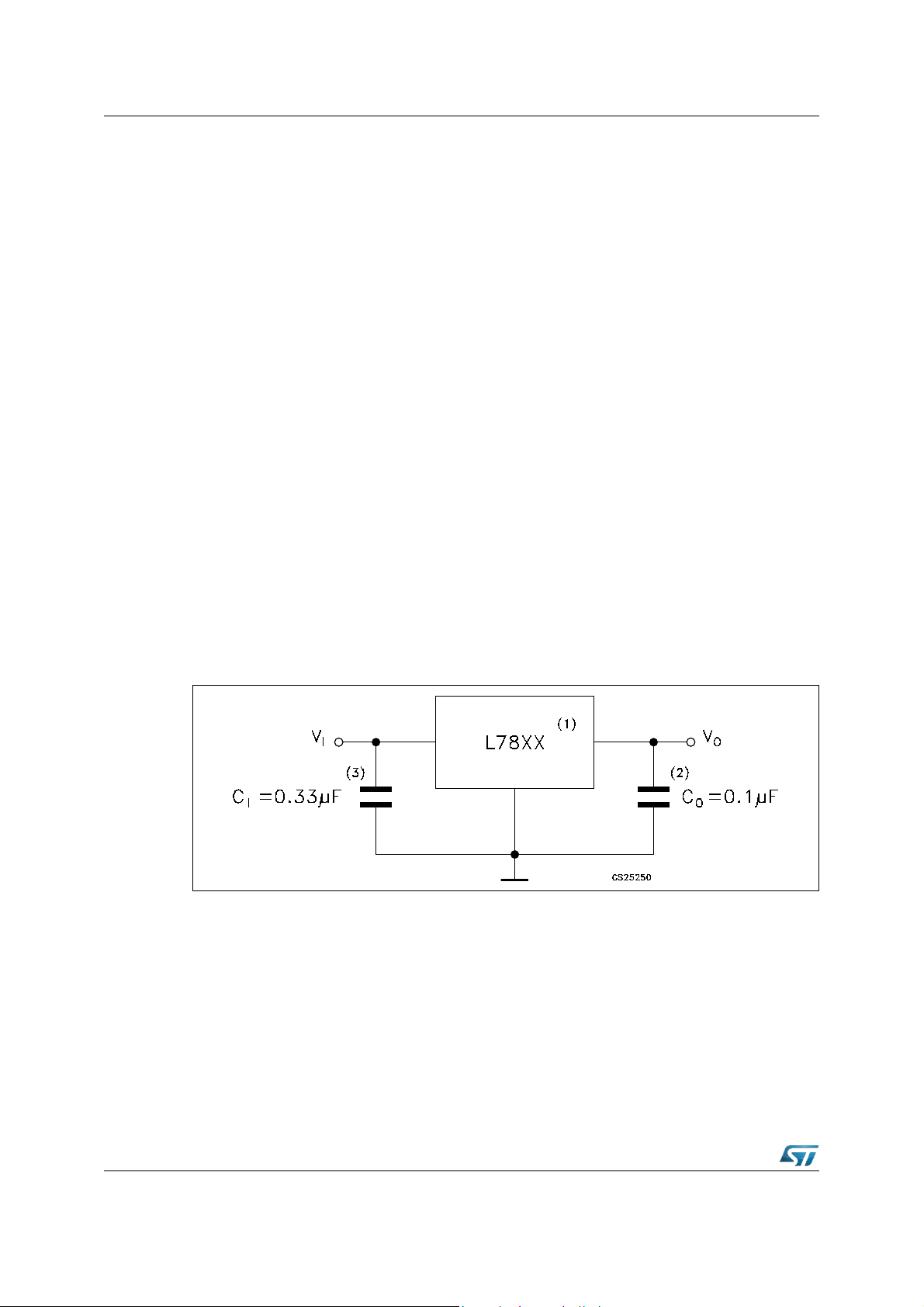
Application information L78xx, L78xxC, L78xxAB, L78xxAC
6 Application information
6.1 Design consideration
The L78xx Series of fixed voltage regulators are designed with thermal overload protection
that shuts down the circuit when subjected to an excessive power overload condition,
internal short-circuit protection that limits the maximum current the circuit will pass, and
output transistor safe-area compensation that reduces the output short-circuit current as the
voltage across the pass transistor is increased. In many low current applications,
compensation capacitors are not required. However, it is recommended that the regulator
input be bypassed with capacitor if the regulator is connected to the power supply filter with
long lengths, or if the output load capacitance is large. An input bypass capacitor should be
selected to provide good high frequency characteristics to insure stable operation under all
load conditions. A 0.33 µF or larger tantalum, mylar or other capacitor having low internal
impedance at high frequencies should be chosen. The byp ass capacitor shou ld be mounted
with the shortest possible leads directly across the regulators input terminals. Normally good
construction techniques should be used to minimize ground loop s and lead resist ance drops
since the regulator has no external sense lead.
The addition of an operational amplifier allows adjustment to higher or intermediate values
while retaining regulation characteristics. The minimum voltag e obtained with the
arrangement is 2 V greater than the regulator voltage.
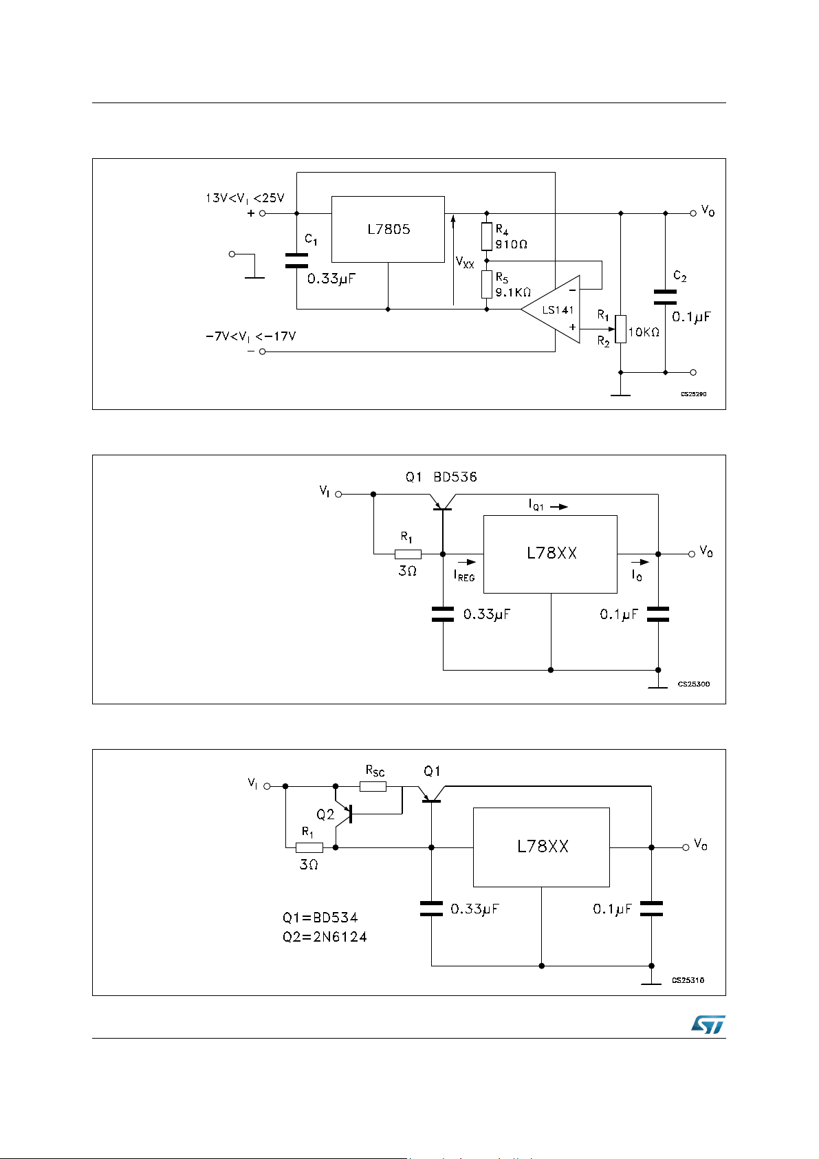
The circuit of Figure 13 can be modified to provide supply protection against short circuit by
adding a short circuit sense resistor, RSC, and an additional PNP transistor. The current
sensing PNP must be able to handle the short circuit current of the three terminal regulator
Therefore a four ampere plastic power transistor is specified.
Figure 8. Fixed output regulator
1. To specify an output voltage, substitute voltage value for "XX".
2. Although no output capacitor is need for stability, it does improve transient response.
3. Required if regulator is locate an appreciable distance from power supply filter.
28/57 DocID2143 Rev 31
Page 29
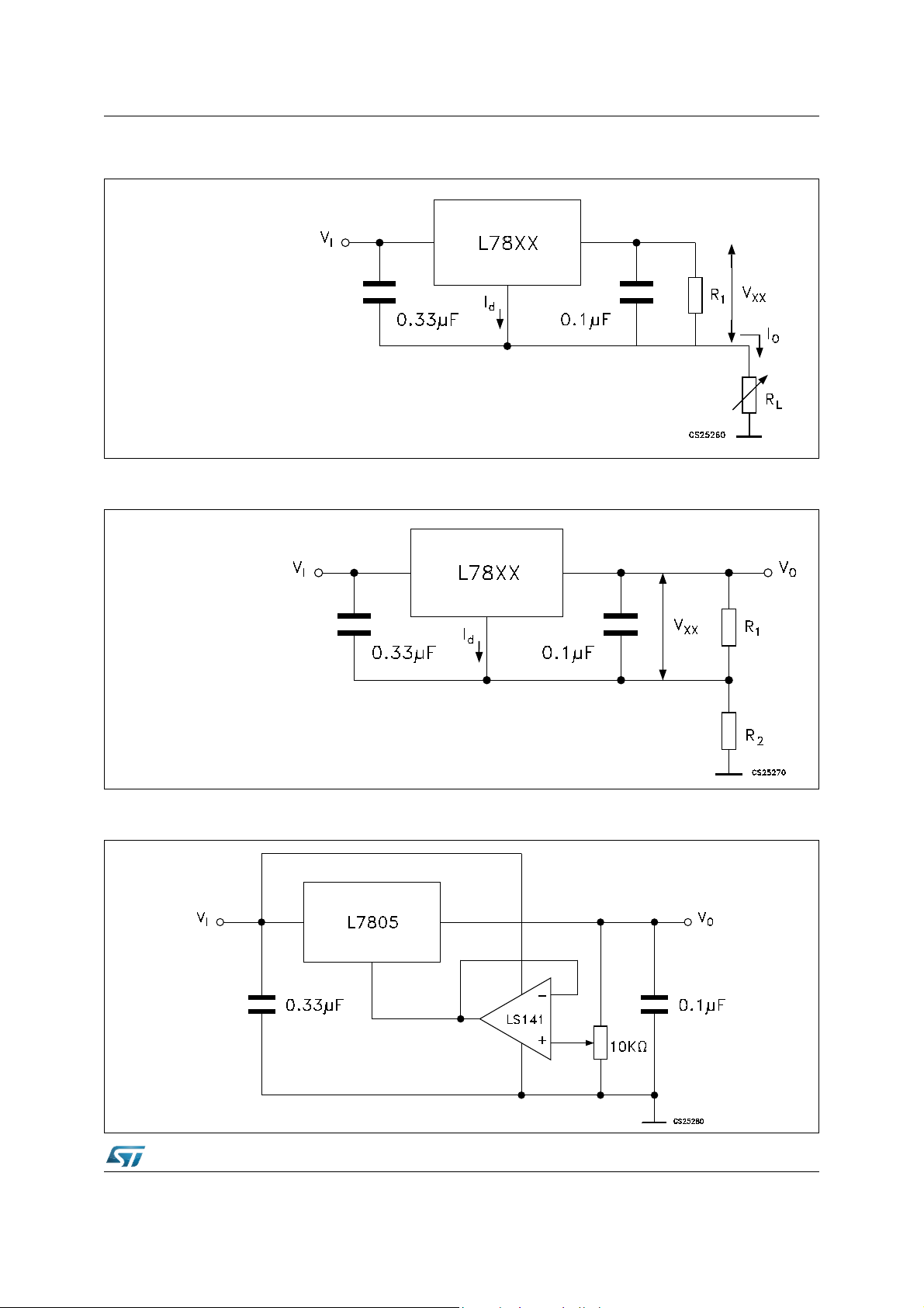
L78xx, L78xxC, L78xxAB, L78xxAC Application information
IO = VXX/R1+I
d
IR1 5 I
d
VO = VXX(1+R2/R1)+IdR
2
Figure 10. Circuit for increasing output voltage
Figure 9. Current regulator
Figure 11. Adjustable output regulator (7 to 30 V)
DocID2143 Rev 31 29/57
Page 30
Application information L78xx, L78xxC, L78xxAB, L78xxAC
VO=VXXR4/R
1
IO = I
REG
+ Q1 (I
REG
______)
V
BEQ1
R
1
R1 = ______________
V
BEQ1
I
REQ
-(IQ1/bQ1)
RSC=V
BEQ2/ISC
Figure 12. 0.5 to 10 V regulator
Figure 13. High current voltage regulator
30/57 DocID2143 Rev 31
Figure 14. High output current with short circuit protection
Page 31
L78xx, L78xxC, L78xxAB, L78xxAC Application information
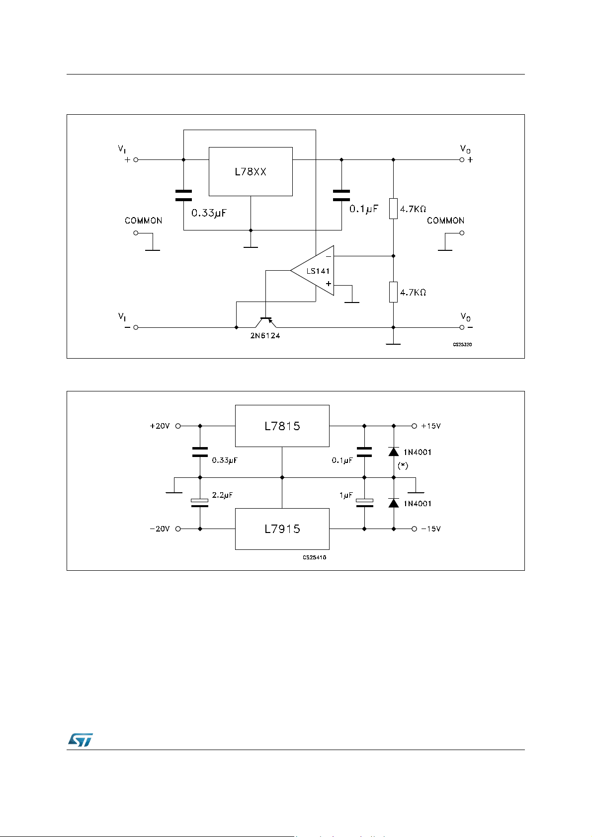
Figure 15. Tracking voltage regulator
Figure 16. Split power supply (± 15 V - 1 A)
* Against potential latch-up problems.
DocID2143 Rev 31 31/57
Page 32
Application information L78xx, L78xxC, L78xxAB, L78xxAC
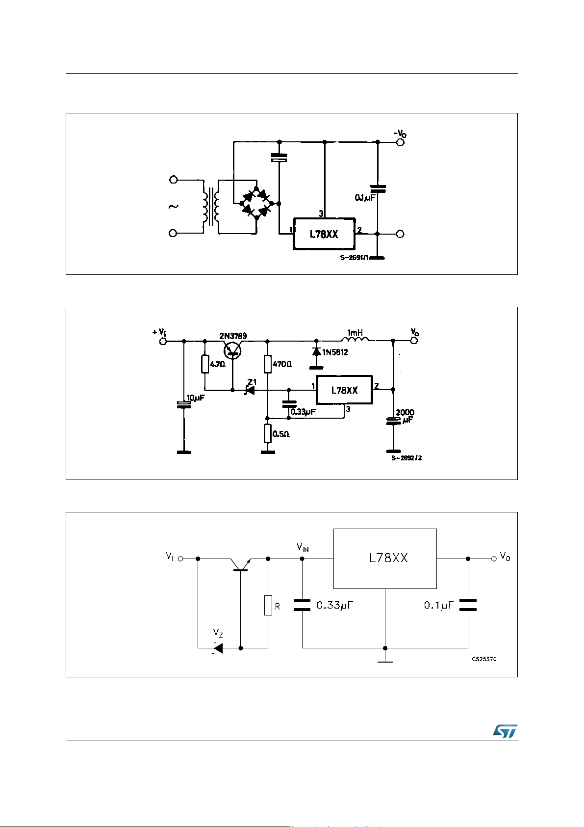
VIN = VI - (VZ + VBE)
Figure 17. Negative output voltage circuit
Figure 18. Switching regulator
Figure 19. High input voltage circuit (configuration 1)
32/57 DocID2143 Rev 31
Page 33
L78xx, L78xxC, L78xxAB, L78xxAC Application information
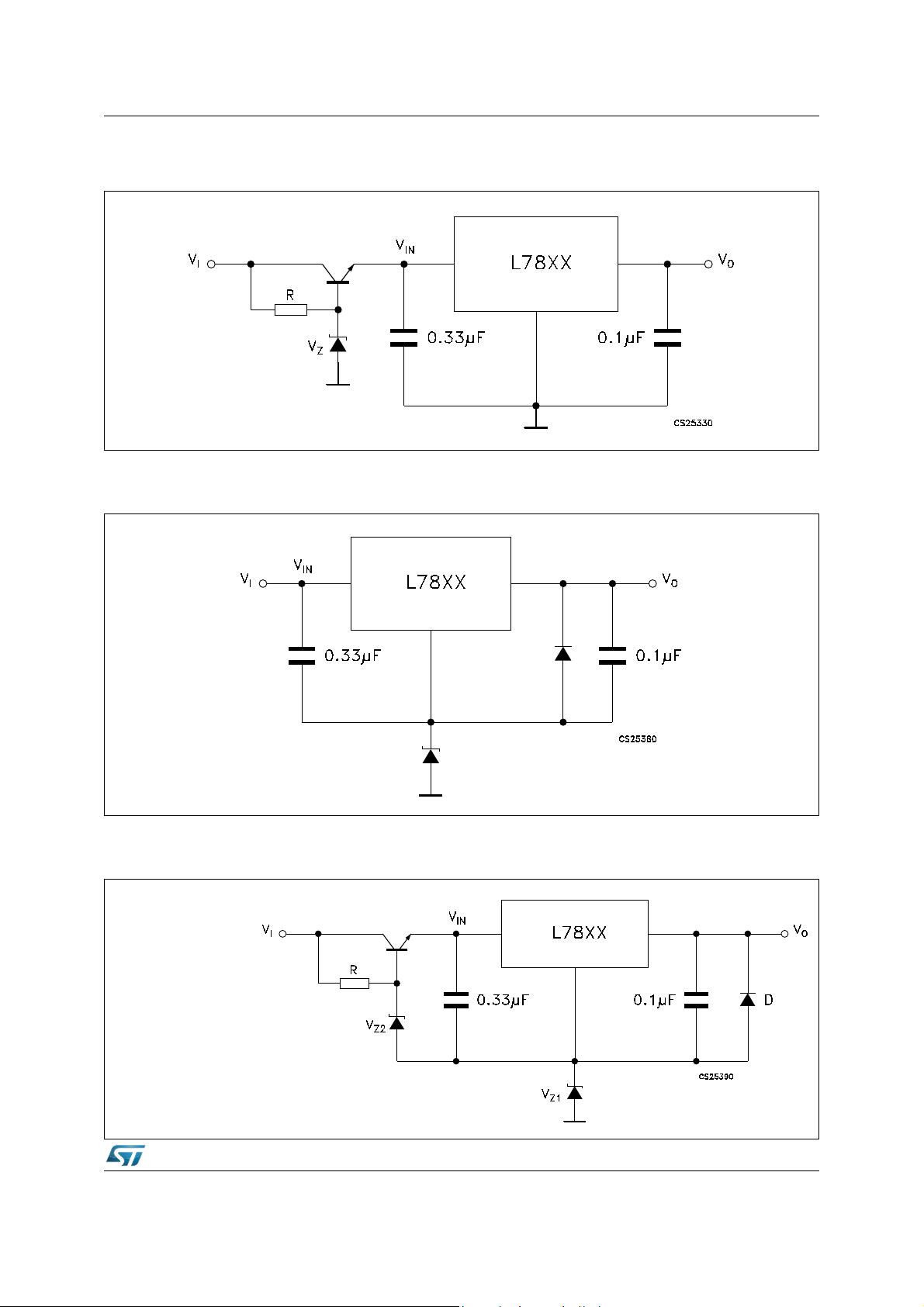
VO = VXX + V
Z1
Figure 20. High input voltage circuit (configuration 2)
Figure 21. High output voltage regulator
Figure 22. High input and output voltage
DocID2143 Rev 31 33/57
Page 34
Application information L78xx, L78xxC, L78xxAB, L78xxAC
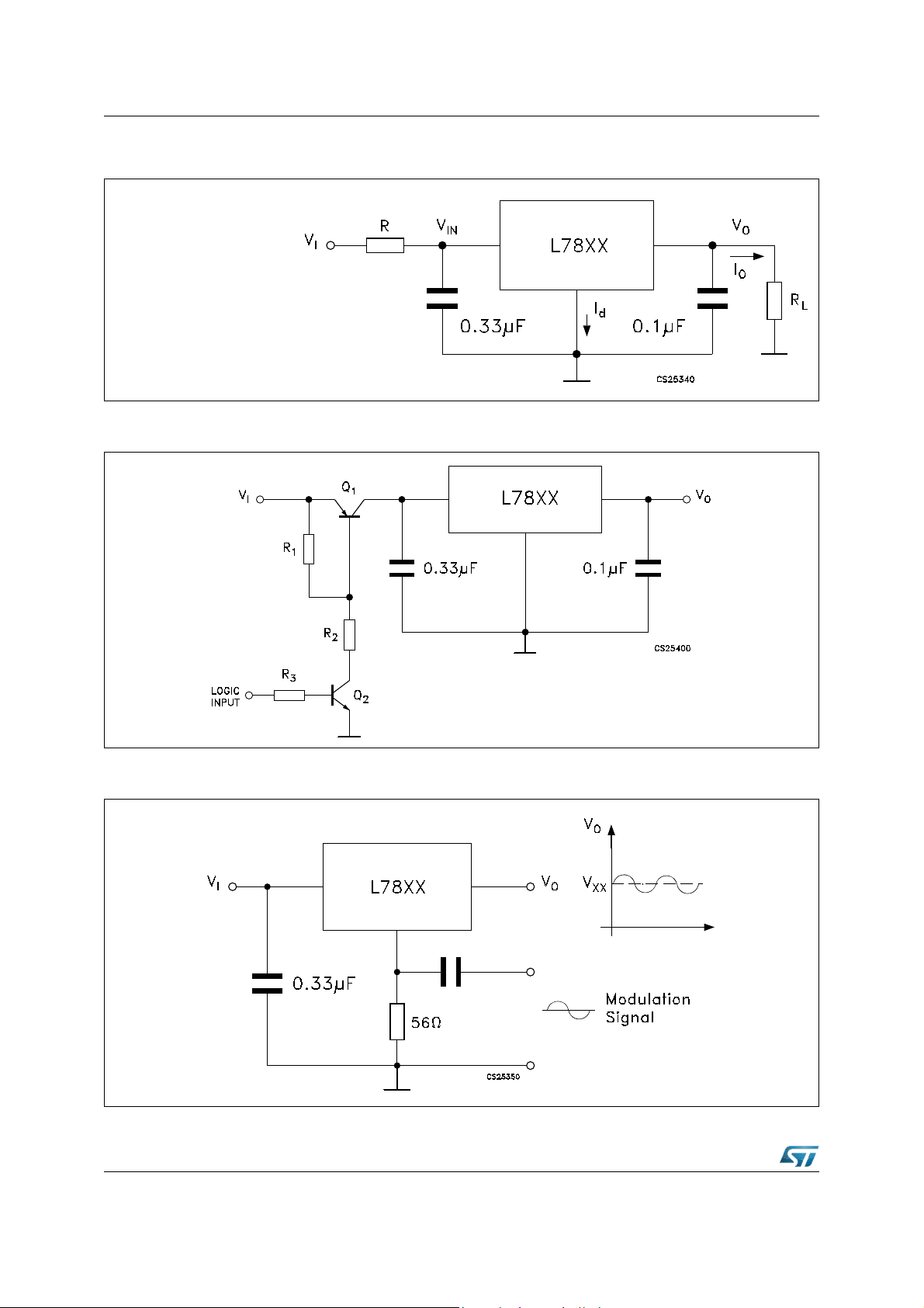
R = ____________________
V
I(min)-VXX-VDROP(max)
I
O(max)+Id(max)
Figure 23. Reducing power dissipation with dropping resistor
Figure 24. Remote shutdown
Figure 25. Power AM modulator (unity voltage gain, IO 0.5)
Note: The circuit performs well up to 100 kHz.
34/57 DocID2143 Rev 31
Page 35
L78xx, L78xxC, L78xxAB, L78xxAC Application information
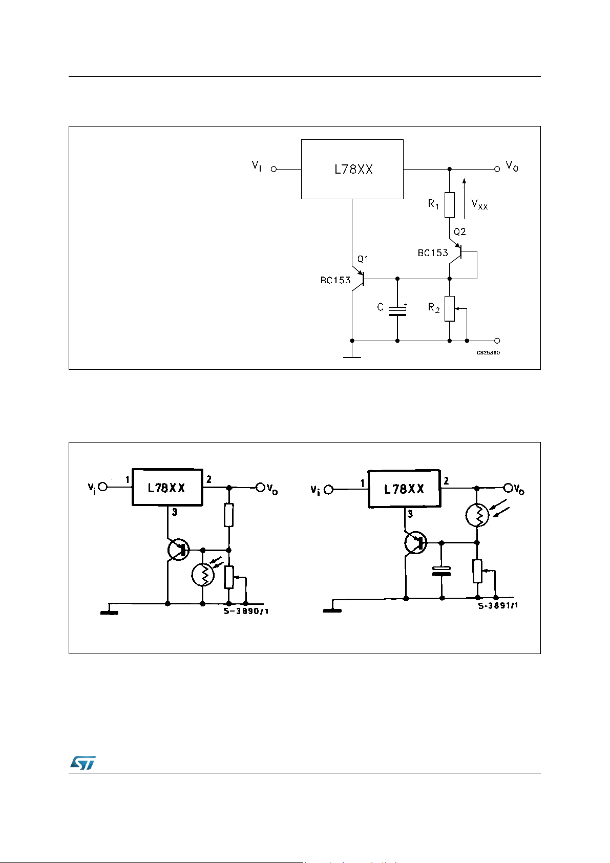
VO = VXX (1+R2/R1) + V
BE
VO rises when the light goes up
VO falls when the light goes up
Figure 26. Adjustable output voltage with temperature compensation
Note: Q2 is connected as a diode in order to compensate the variation of the Q1 VBE with the
temperature. C allows a slow rise time of the V
.
O
Figure 27. Light controllers (V
= VXX + VBE)
O(min)
DocID2143 Rev 31 35/57
Page 36
Application information L78xx, L78xxC, L78xxAB, L78xxAC
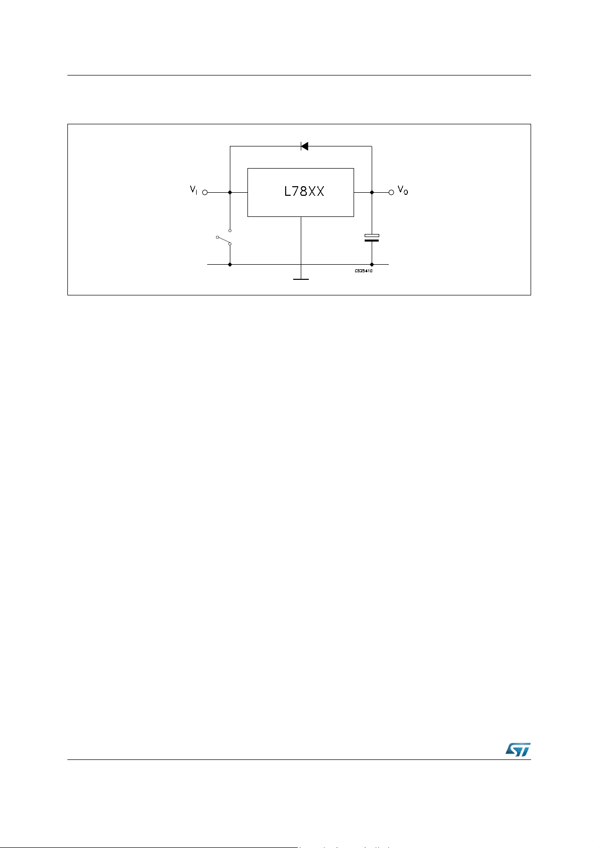
Figure 28. Protection against input short-circuit with high capacitance loads
Note: Application with high capacitance loads and an output voltage greater than 6 volts need an
external diode (see Figure 23 on p age 34) to protect the device against input short circuit. In
this case the input voltage falls rapidly while the output voltage decrease slowly. The
capacitance discharges by means of the base-emitter junction of the series pass tr ansistor
in the regulator. If the energy is sufficiently high, the transistor may be destroyed. The
external diode by-passes the current from the IC to ground.
36/57 DocID2143 Rev 31
Page 37
L78xx, L78xxC, L78xxAB, L78xxAC Typical performance
7 Typical performance
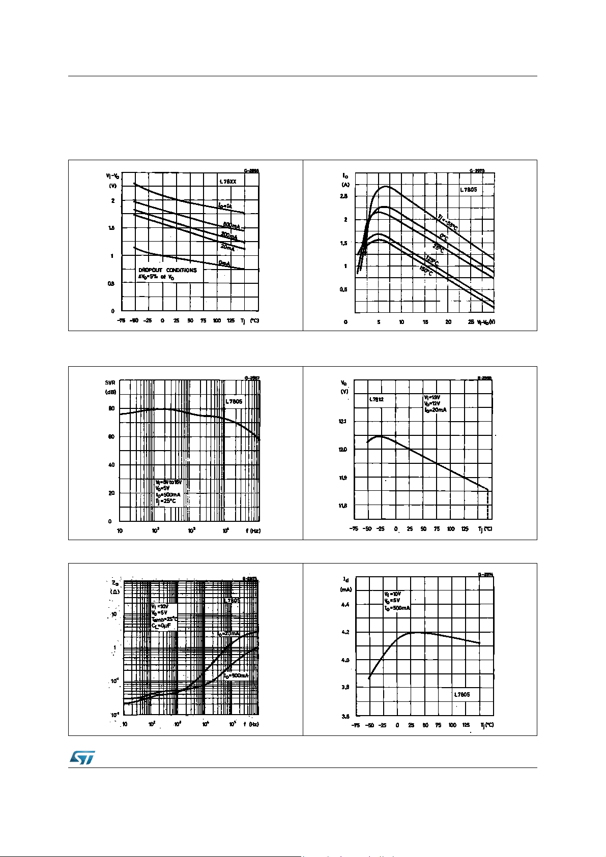
Figure 29. Dropout voltage vs. junction
temperature
Figure 31. Supply voltage rejection vs.
frequency
Figure 30. Peak output current vs. input/output
differential voltage
Figure 32. Output voltage vs. junction
temperature
Figure 33. Output impedance vs. frequency Figure 34. Quiescent current vs. junction temp.
DocID2143 Rev 31 37/57
Page 38
Typical performance L78xx, L78xxC, L78xxAB, L78xxAC
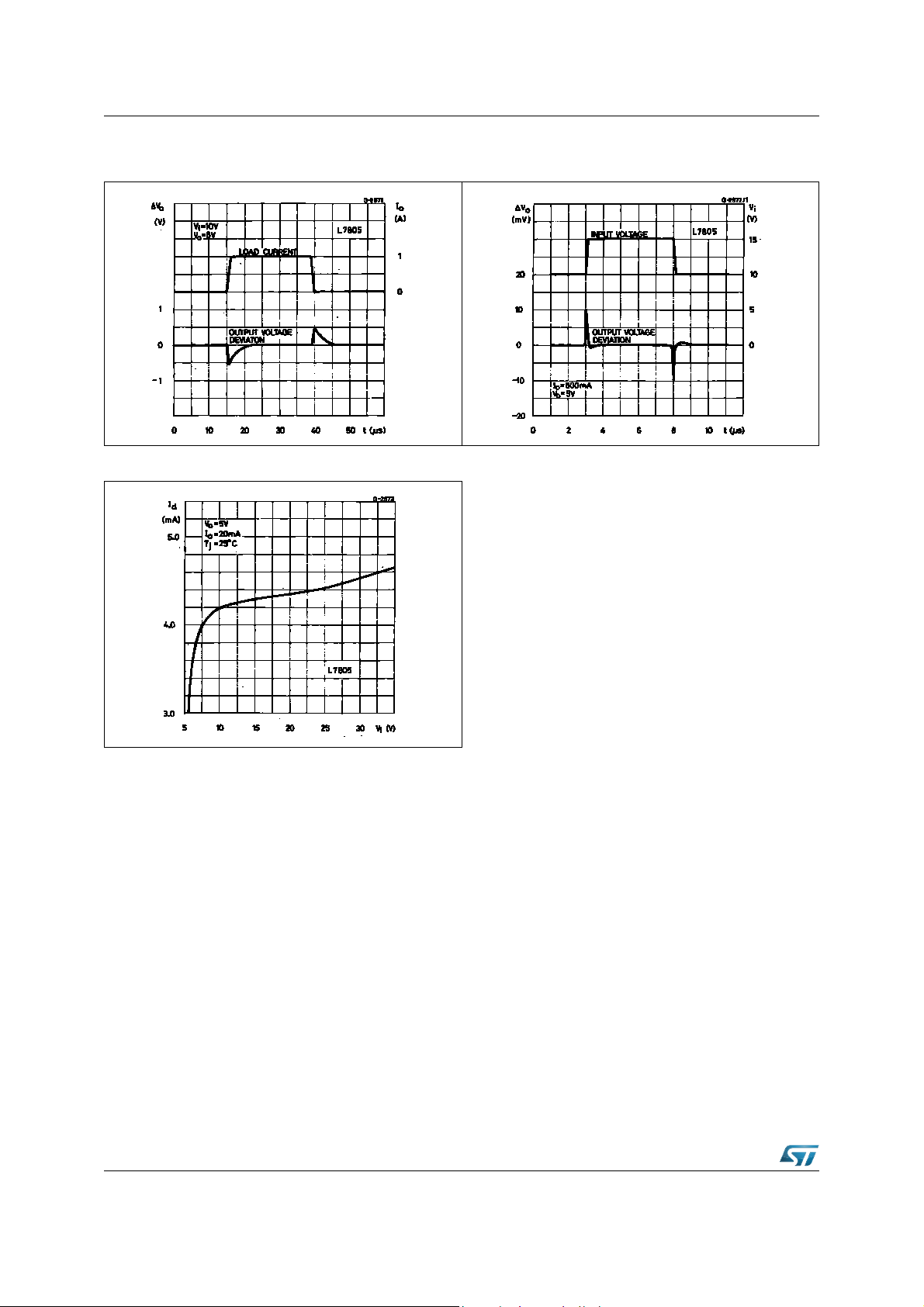
Figure 35. Load transient response Figure 36. Line transient response
Figure 37. Quiescent current vs. input voltage
38/57 DocID2143 Rev 31
Page 39
L78xx, L78xxC, L78xxAB, L78xxAC Package mechanical data
8 Package mechanical data
In order to meet environmental requirements, ST offers these devices in different grades of
ECOPACK
specifications, grade definitions and product status are available at: www.st.com.
ECOPACK
®
packages, depending on their level of environmental compliance. ECOPACK®
®
is an ST trademark.
Table 23. TO-220 mechanical data
Type STD - ST Dual Gauge Type STD - ST Single Gauge
Dim.
Min. Typ. Max. Min. Typ. Max.
A 4.40 4.60 4.40 4.60
b 0.61 0.88 0.61 0.88
b1 1.14 1.70 1.14 1.70
c 0.48 0.70 0.48 0.70
D 15.25 15.75 15.25 15.75
D1 1.27
E 10.00 10.40 10.00 10.40
mm. mm.
e 2.40 2.70 2.40 2.70
e1 4.95 5.15 4.95 5.15
F 1.23 1.32 0.51 0.60
H1 6.20 6.60 6.20 6.60
J1 2.40 2.72 2.40 2.72
L 13.00 14.00 13.00 14.00
L1 3.50 3.93 3.50 3.93
L20 16.40 16.40
L30 28.90 28.90
P 3.75 3.85 3.75 3.85
Q 2.65 2.95 2.65 2.95
In spite of some difference in tolerances, the packages are compatible.
DocID2143 Rev 31 39/57
Page 40
Package mechanical data L78xx, L78xxC, L78xxAB, L78xxAC
0015988_S
Figure 38. Drawing dimension TO-220 (type STD-ST Dual Gauge)
Note: 1 Maximum resin gate protrusion: 0.5 mm.
2 Resin gate position is accepted in each of the two positions shown on the drawing, or their
symmetrical.
40/57 DocID2143 Rev 31
Page 41
L78xx, L78xxC, L78xxAB, L78xxAC Package mechanical data
8174627_B
Figure 39. Drawing dimension TO-220 (type STD-ST Single Gauge)
DocID2143 Rev 31 41/57
Page 42
Package mechanical data L78xx, L78xxC, L78xxAB, L78xxAC
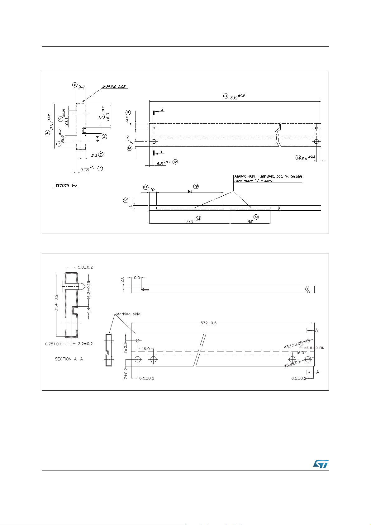
Figure 40. Drawing dimension tube for TO-220 Dual Gauge (mm.)
Figure 41. Drawing dimension tube for TO-220 Single Gauge (mm.)
42/57 DocID2143 Rev 31
Page 43
L78xx, L78xxC, L78xxAB, L78xxAC Package mechanical data
7012510A-H
Figure 42. Drawing dimension TO-220FP
DocID2143 Rev 31 43/57
Page 44
Package mechanical data L78xx, L78xxC, L78xxAB, L78xxAC
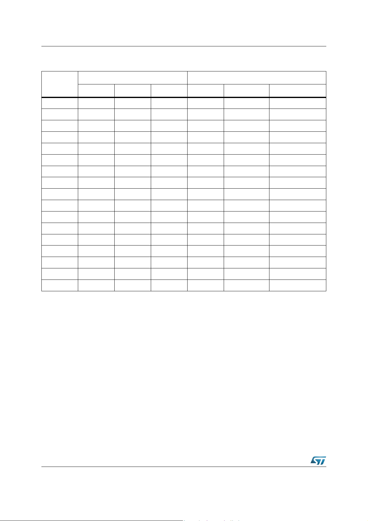
Table 24. TO-220FP mechanical data
mm. inch.
Dim.
Min. Typ. Max. Min. Typ. Max.
A 4.40 4.60 0.173 0.181
B 2.5 2.7 0.098 0.106
D 2.5 2.75 0.098 0.108
E 0.45 0.70 0.017 0.027
F 0.75 1 0.030 0.039
F1 1.15 1.50 0.045 0.059
F2 1.15 1.50 0.045 0.059
G 4.95 5.2 0.194 0.204
G1 2.4 2.7 0.094 0.106
H 10.0 10.40 0.393 0.409
L2 16 0.630
L3 28.6 30.6 1.126 1.204
L4 9.8 10.6 0.385 0.417
L5 2.9 3.6 0.114 0.142
L6 15.9 16.4 0.626 0.645
L7 9 9.3 0.354 0.366
DIA. 3 3.2 0.118 0.126
44/57 DocID2143 Rev 31
Page 45
L78xx, L78xxC, L78xxAB, L78xxAC Package mechanical data
E
B
R
C
D
A
P
G
N
V
U
O
P003C/C
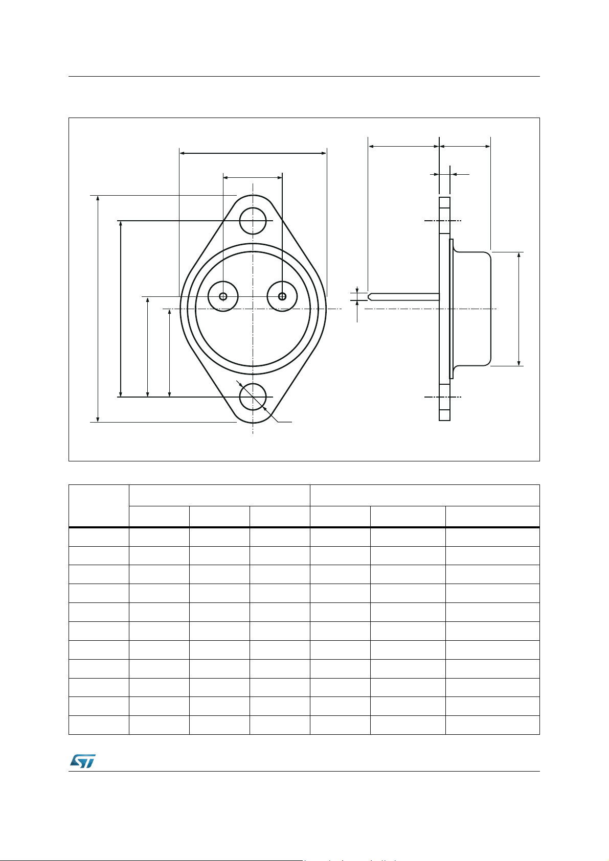
Figure 43. Drawing dimension TO-3
Table 25. TO-3 mechanical data
mm. inch.
Dim.
Min. Typ. Max. Min. Typ. Max.
A 11.85 0.466
B 0.96 1.05 1.10 0.037 0.041 0.043
C 1.70 0.066
D 8.7 0.342
E 20.0 0.787
G 10.9 0.429
N 16.9 0.665
P 26.2 1.031
R 3.88 4.09 0.152 0.161
U 39.5 1.555
V 30.10 1.185
DocID2143 Rev 31 45/57
Page 46
Package mechanical data L78xx, L78xxC, L78xxAB, L78xxAC
0068772-F
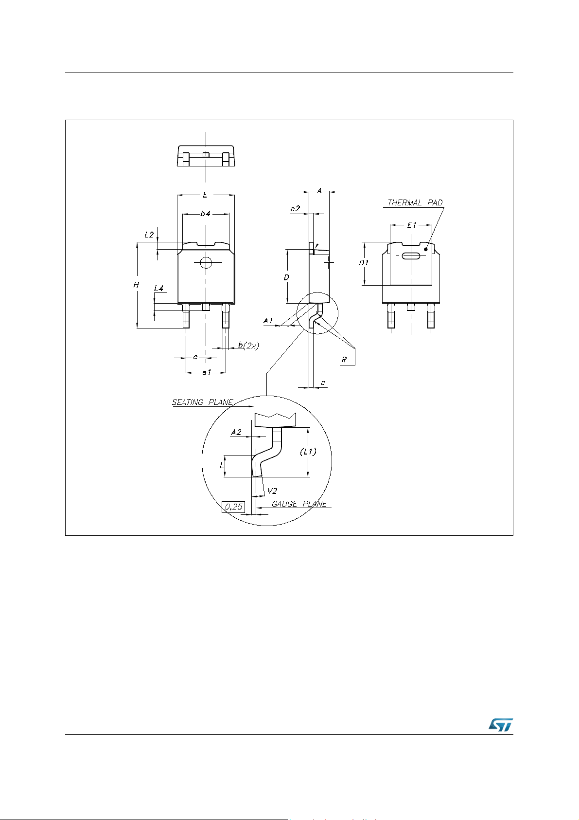
Figure 44. Drawing dimension DPAK
46/57 DocID2143 Rev 31
Page 47
L78xx, L78xxC, L78xxAB, L78xxAC Package mechanical data
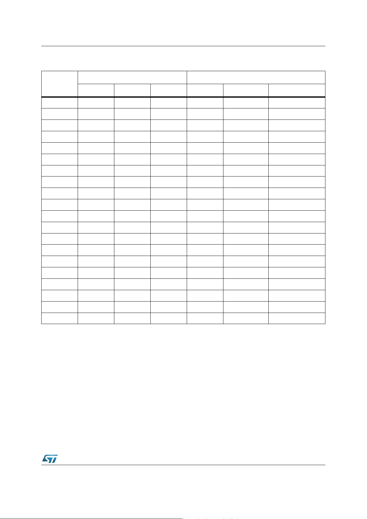
Table 26. DPAK mechanical dat a
mm. inch.
Dim.
Min. Typ. Max. Min. Typ. Max.
A 2.2 2.4 0.086 0.094
A1 0.9 1.1 0.035 0.043
A2 0.03 0.23 0.001 0.009
B 0.64 0.9 0.025 0.035
b4 5.2 5.4 0.204 0.212
C 0.45 0.6 0.017 0.023
C2 0.48 0.6 0.019 0.023
D 6 6.2 0.236 0.244
D1 5.1 0.200
E 6.4 6.6 0.252 0.260
E1 4.7 0.185
e2.28 0.090
e1 4.4 4.6 0.173 0.181
H 9.35 10.1 0.368 0.397
L 1 0.039
(L1) 2.8 0.110
L2 0.8 0.031
L4 0.6 1 0.023 0.039
R0.2 0.008
V2 0° 8° 0° 8°
DocID2143 Rev 31 47/57
Page 48
Package mechanical data L78xx, L78xxC, L78xxAB, L78xxAC
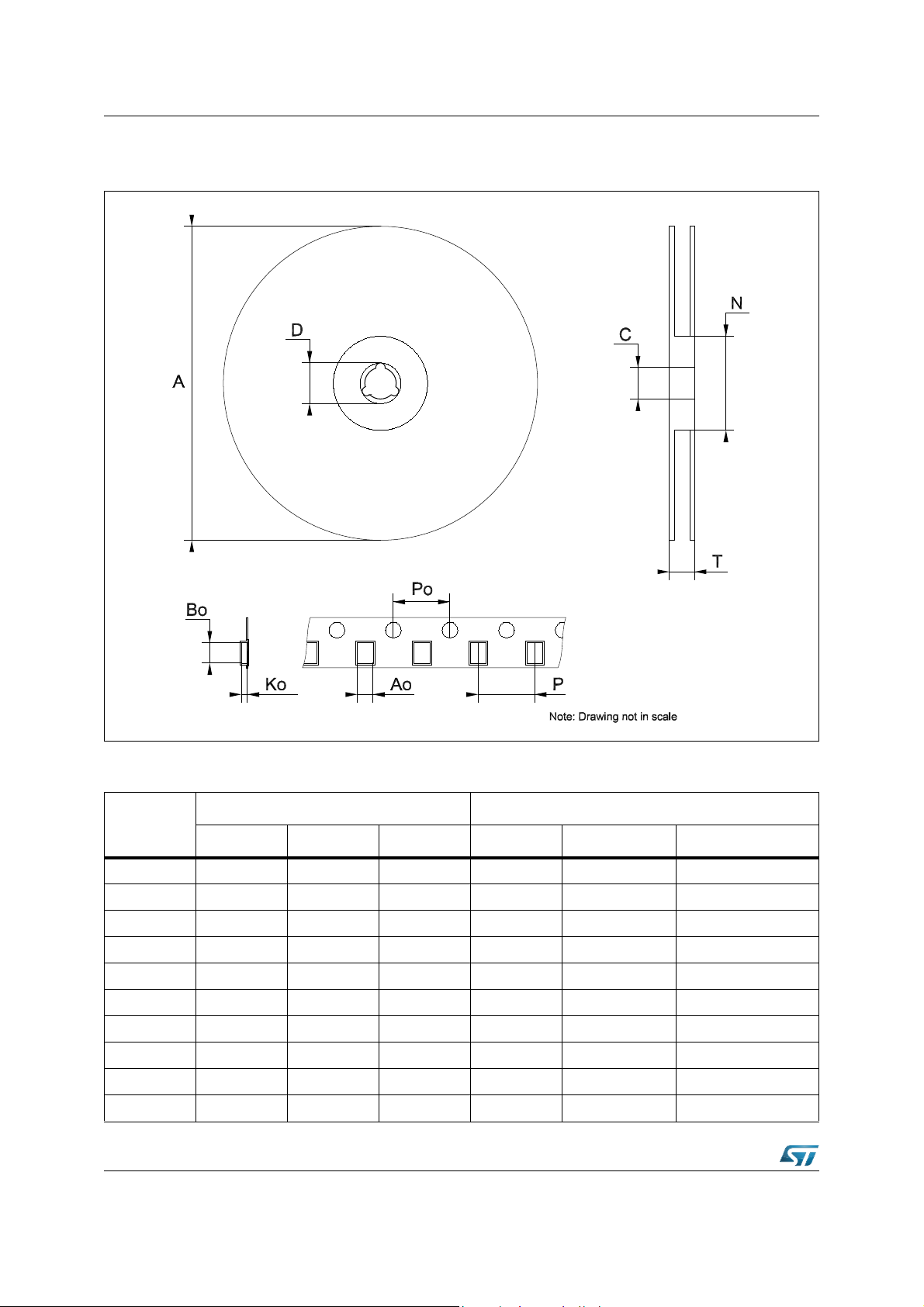
Figure 45. Drawing dimension tape and reel for DPAK
Table 27. Tape and reel DPAK mechanical data
mm. inch.
Dim.
Min. Typ. Max. Min. Typ. Max.
A 330 12.992
C 12.8 13.0 13.2 0.504 0.512 0.519
D 20.2 0.795
N 60 2.362
T 22.4 0.882
Ao 6.80 6.90 7.00 0.268 0.272 0.2.76
Bo 10.40 10.50 10.60 0.409 0.413 0.417
Ko 2.55 2.65 2.75 0.100 0.104 0.105
Po 3.9 4.0 4.1 0.153 0.157 0.161
P 7.9 8.0 8.1 0.311 0.315 0.319
48/57 DocID2143 Rev 31
Page 49
L78xx, L78xxC, L78xxAB, L78xxAC Package mechanical data
0079457/L
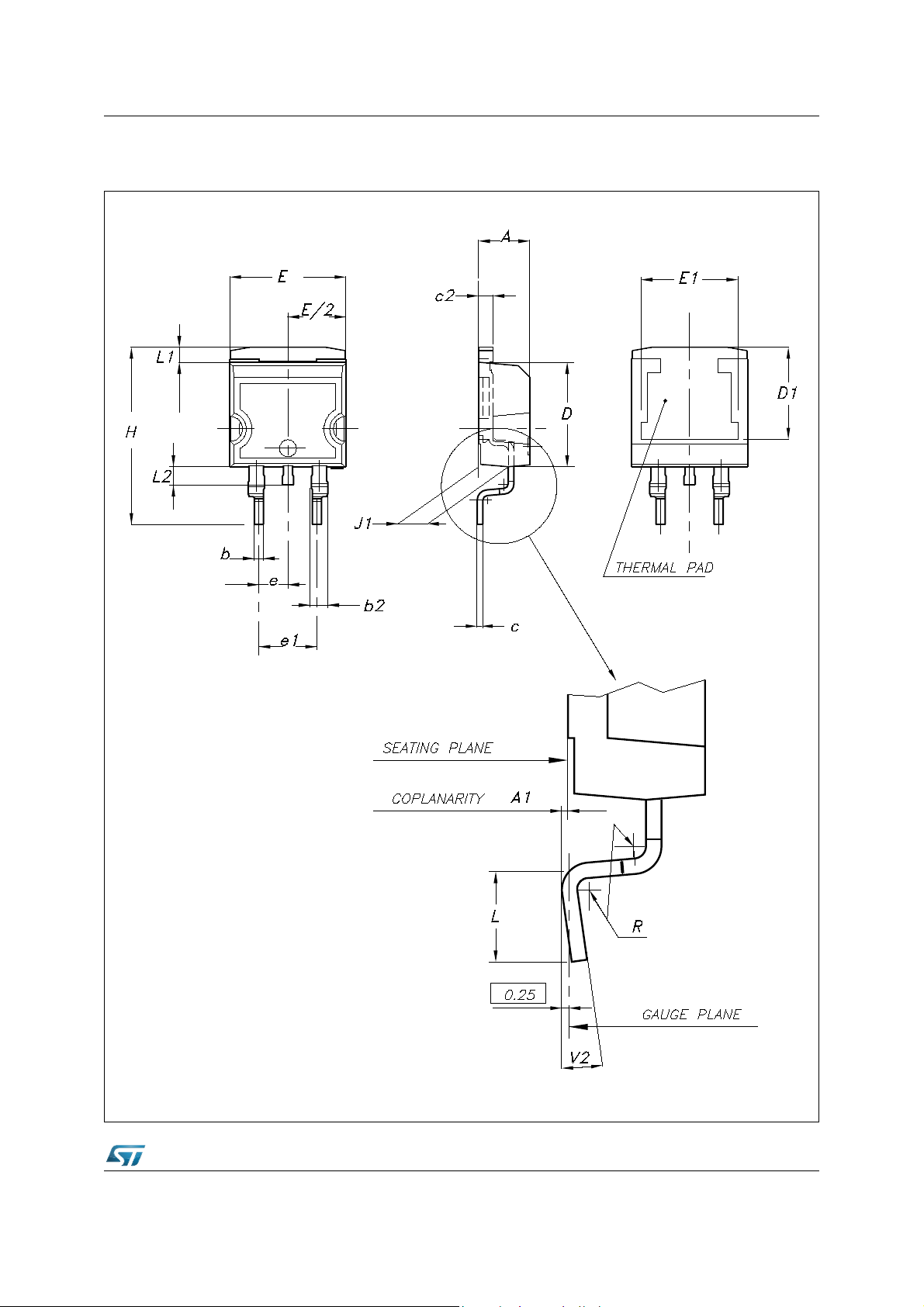
Figure 46. Drawing dimension D²PAK (type STD-ST)
DocID2143 Rev 31 49/57
Page 50
Package mechanical data L78xx, L78xxC, L78xxAB, L78xxAC
0079457/L
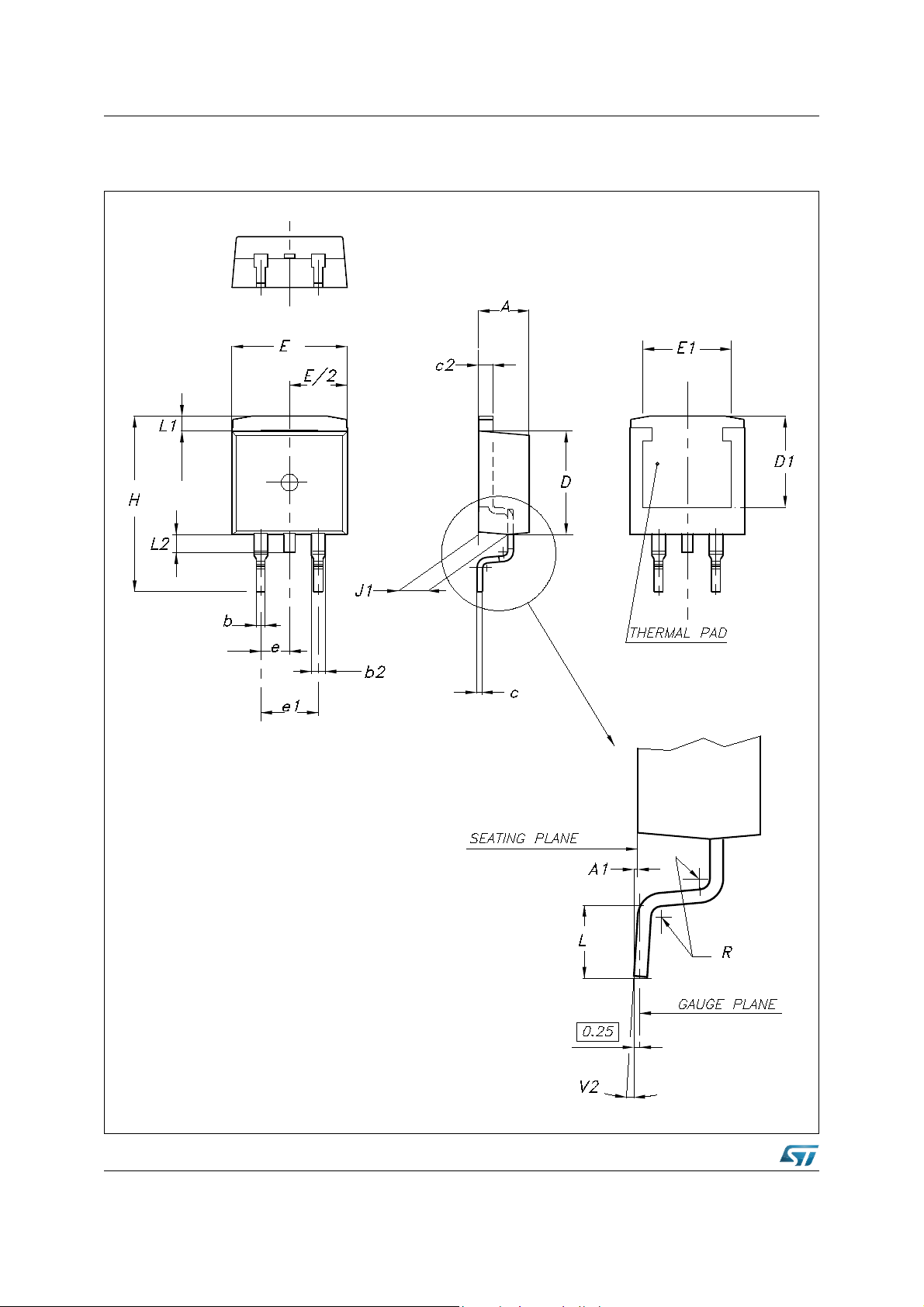
Figure 47. Drawing dimension D²PAK (type WOOSEOK-Subcon.)
50/57 DocID2143 Rev 31
Page 51
L78xx, L78xxC, L78xxAB, L78xxAC Package mechanical data
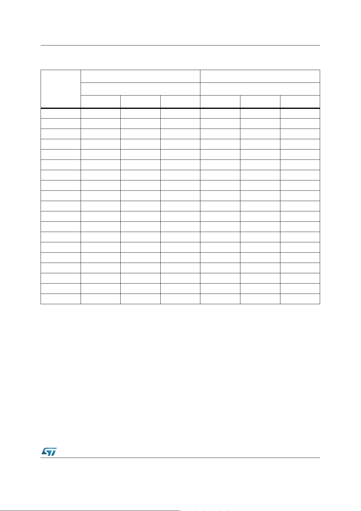
Table 28. D²PAK mechanical data
Type STD-ST Type WOOSEOK-Subcon.
Dim.
Min. Typ. Max. Min. Typ. Max.
A 4.40 4.60 4.30 4.70
A1 0.03 0.23 0 0.20
b 0.70 0.93 0.70 0.90
b2 1.14 1.70 1.17 1.37
c 0.45 0.60 0.45 0.50 0.60
c2 1.23 1.36 1.25 1.30 1.40
D 8.95 9.35 9 9.20 9.40
D1 7.50 7.50
E 10 10.40 9.80 10.20
E1 8.50 7.50
e2.54 2.54
e1 4.88 5.28 5.08
H 15 15.85 15 15.30 15.60
J1 2.49 2.69 2.20 2.60
L 2.29 2.79 1.79 2.79
mm. mm.
L1 1.27 1.40 1 1.40
L2 1.30 1.75 1.20 1.60
R 0.4 0.30
V2 0° 8° 0° 3°
Note: The D²PAK package coming from the subcontractor Wooseok is fully compatible with the
ST's package suggested footprint.
DocID2143 Rev 31 51/57
Page 52
Package mechanical data L78xx, L78xxC, L78xxAB, L78xxAC
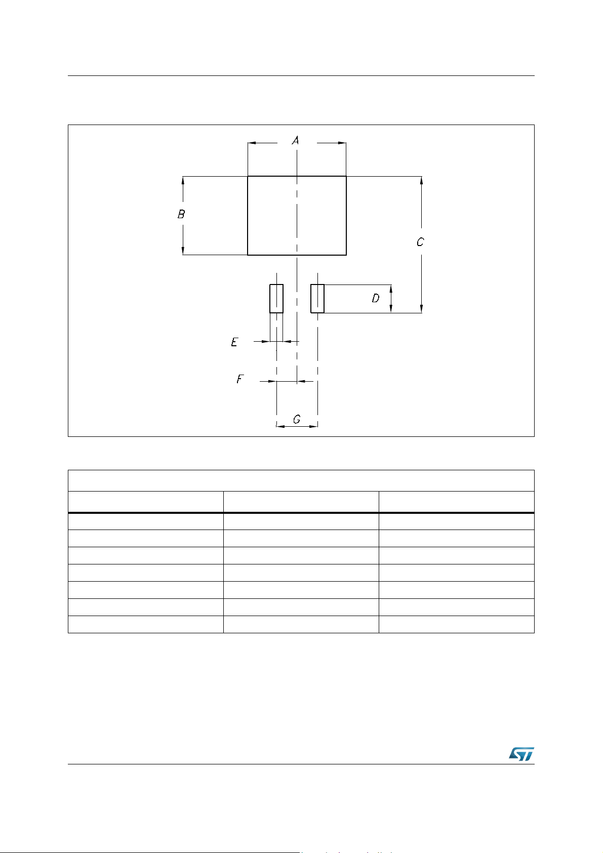
Figure 48. D²PAK footprint recommended data
Table 29. D²PAK footprint data
Values
Dim. mm. inch.
A 12.20 0.480
B9.750.384
C 16.90 0.665
D3.500.138
E1.600.063
F2.540.100
G5.080.200
52/57 DocID2143 Rev 31
Page 53
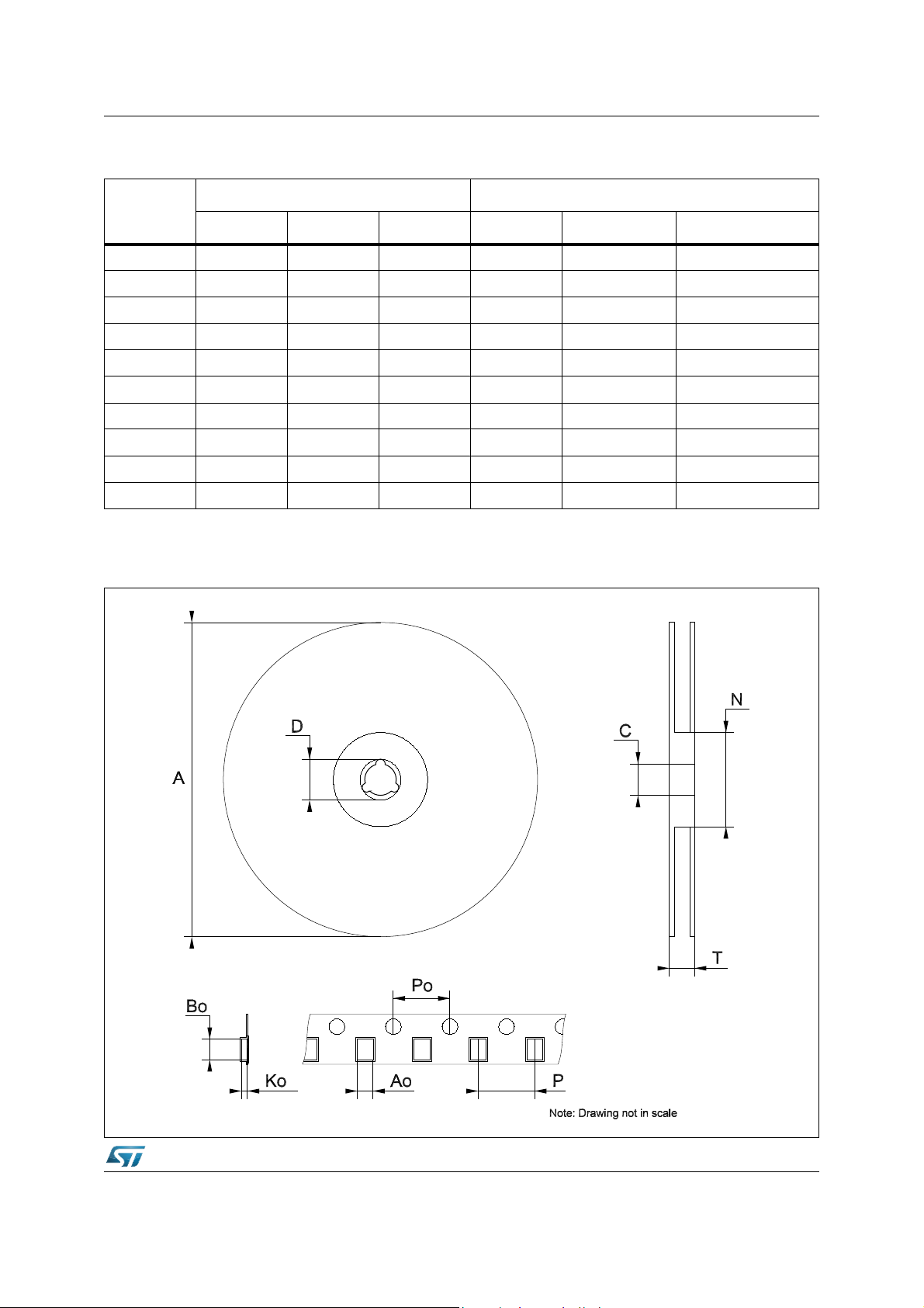
L78xx, L78xxC, L78xxAB, L78xxAC Package mechanical data
Table 30. Tape and reel D²PAK mechanical data
mm. inch.
Dim.
Min. Typ. Max. Min. Typ. Max.
A 180 7.086
C 12.8 13.0 13.2 0.504 0.512 0.519
D 20.2 0.795
N 60 2.362
T 14.4 0.567
Ao 10.50 10.6 10.70 0.413 0.417 0.421
Bo 15.70 15.80 15.90 0.618 0.622 0.626
Ko 4.80 4.90 5.00 0.189 0.193 0.197
Po 3.9 4.0 4.1 0.153 0.157 0.161
P 11.9 12.0 12.1 0.468 0.472 0.476
Figure 49. Drawing dimension tape and reel for D²PAK
DocID2143 Rev 31 53/57
Page 54
Order codes L78xx, L78xxC, L78xxAB, L78xxAC
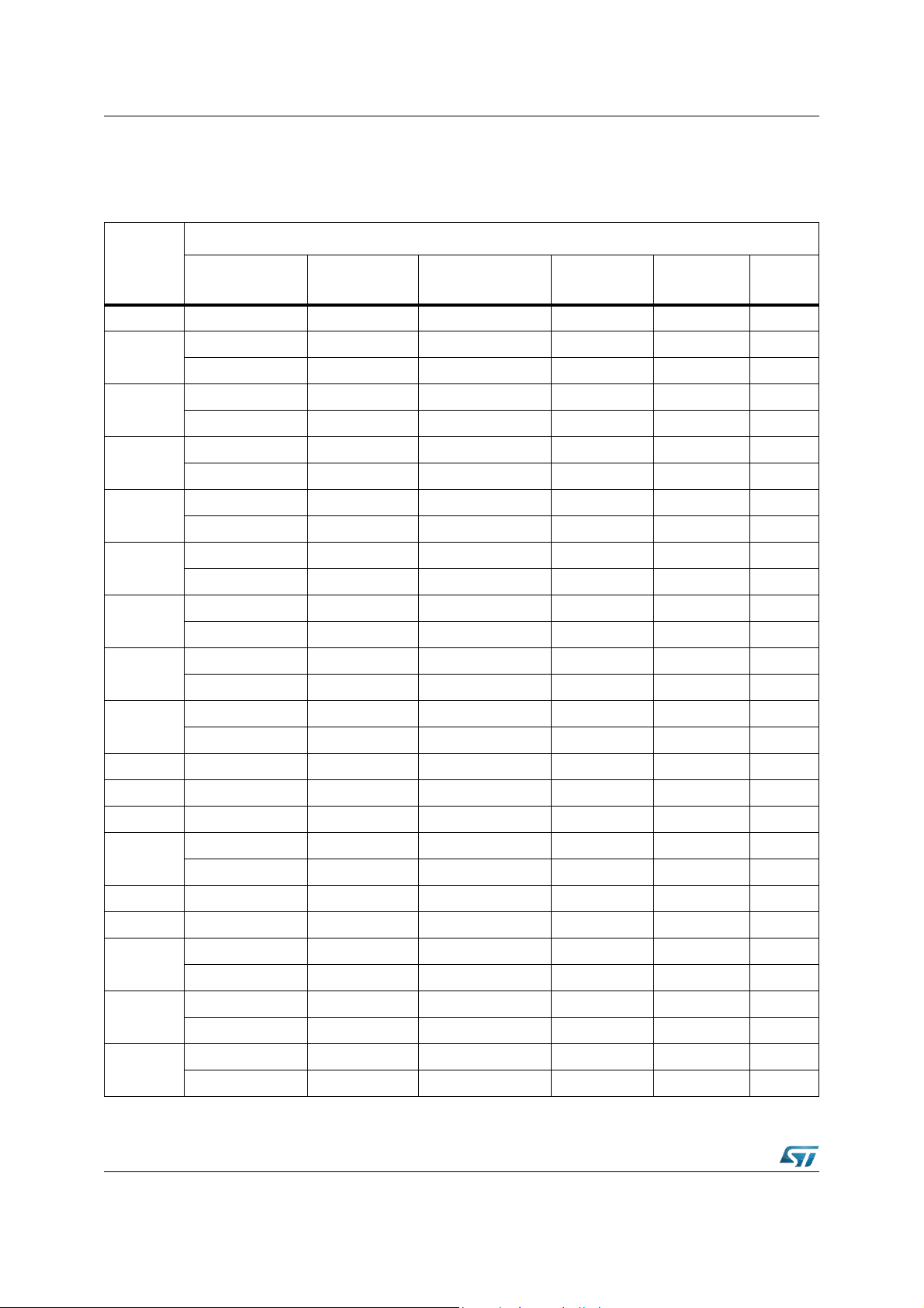
9 Order codes
T able 31. Order codes
Order codes
Part
numbers
TO-220 DPAK D²PAK TO-220FP TO-3
L7805 L7805T 5 V
Output
voltages
L7805C
L7805CV-DG
(1)
5 V
L7805ABV L7805ABD2T-TR L7805ABP 5 V
L7805CV L7805CDT-TR L7805CD2T-TR L7805CP L7805CT 5 V
L7805AB
L7805ABV-DG
(1)
5 V
L7805ACV L7805ACD2T-TR L7805ACP 5 V
L7805AC
L7805ACV-DG
(1)
5 V
L7806CV L7806CD2T-TR L7806CT 6 V
L7806C
L7806CV-DG
(1)
6 V
L7806ABV L7806ABD2T-TR 6 V
L7806AB
L7806ABV-DG
(1)
6 V
L7806ACV 6 V
L7806AC
L7806ACV-DG
(1)
6 V
L7808CV L7808CD2T-TR 8 V
L7808C
L7808CV-DG
(1)
8 V
L7808ABV L7808ABD2T-TR 8 V
L7808AB
L7808ABV-DG
(1)
8 V
L7808AC L7808ACV 8 V
L7808ACV-DG
(1)
L7885C L7885CV L7885CD2T-TR
(2)
L7885CP
(2)
L7885CT
(2)
8 V
8.5 V
L7809CV L7809CD2T-TR L7809CP 9 V
L7809C
L7809CV-DG
(1)
9 V
L7809AB L7809ABV L7809ABD2T-TR 9 V
L7809AC L7809ACV 9 V
L7812C
L7812CV-DG
(1)
L7812ABV L7812ABD2T-TR 12 V
L7812CV L7812CD2T-TR L7812CP L7812CT 12 V
L7812AB
L7812ABV-DG
(1)
L7812ACV L7812ACD2T-TR 12 V
L7812AC
L7812ACV-DG
(1)
54/57 DocID2143 Rev 31
12 V
12 V
12 V
Page 55
L78xx, L78xxC, L78xxAB, L78xxAC Order codes
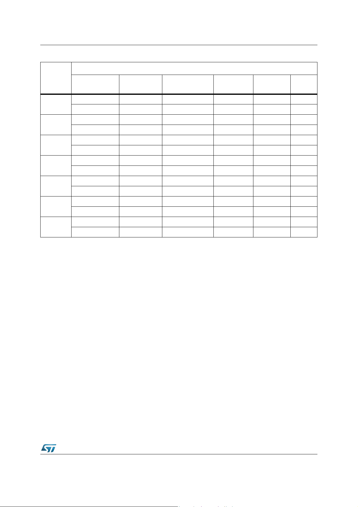
T able 31. Order codes
Order codes
Part
numbers
TO-220 DPAK D²PAK TO-220FP TO-3
Output
voltages
L7815C
L7815CV L7815CD2T-TR L7815CP L7815CT 15 V
L7815CV-DG
L7815ABV L7815ABD2T-TR 15 V
L7815AB
L7815ABV-DG
L7815ACV L7815ACD2T-TR 15 V
L7815AC
L7815ACV-DG
L7818CV L7818CD2T-TR
L7818C
L7818CV-DG
L7824CV L7824CD2T-TR L7824CP L7824CT 24 V
L7824C
L7824CV-DG
L7824ABV 24 V
L7824AB
L7824ABV-DG
L7824ACV 24 V
L7824AC
L7824ACV-DG
1. TO-220 Dual Gauge frame.
2. Available on request.
(1)
(1)
(1)
(1)
(1)
(1)
(1)
(2)
15 V
15 V
15 V
L7818CT 18 V
18 V
24 V
24 V
24 V
DocID2143 Rev 31 55/57
Page 56
Revision history L78xx, L78xxC, L78xxAB, L78xxAC
10 Revision history
Table 32. Document revision history
Date Revision Changes
21-Jun-2004 12 Document updating.
03-Aug-2006 13 Order codes has been updated and new template.
19-Jan-2007 14 D²PAK mechanical data has been updated and add footprint data.
31-May-2007 15 Order codes has been updated.
29-Aug-2007 16 Added Table 1 in cover page.
11-Dec-2007 17 Modified: Table 31.
06-Feb-2008 18
Added: TO-220 mechanical data Figure 38 on page 40 , Figure 39 on page 41,
and Table 23 on page 39. Modified: Table 31 on page 54.
18-Mar-2008 19
26-Jan-2010 20
04-Mar-2010 21 Added notes Figure 38 on page 40.
08-Sep-2010 22 Modified Table 31 on page 54.
23-Nov-2010 23 Added: T
16-Sep-2011 24 Modified title on page 1.
30-Nov-2011 25
08-Feb-2012 26
27-Mar-2012 27 Added: order codes L7812ABV-DG, L7815ABV-DG Table 31 on page 54.
27-Apr-2012 28
10-May-2012 29
19-Sep-2012 30 Modified load regulation units from V to mV in Table 5 to Table 11.
Added: Table 26: D PAK mechanical data on page 47, Table 27: Tape and reel
DPAK mechanical data on page 48. Modified: Table 31 on page 54.
Modified Table1 on page 1 and Table 23 on p a g e39, added: Figure 38 on
page 40 and Figure 39 on page 41, Figure 40 on page 42 and Figure 41 on
page 42.
= 25 °C test condition in VO on Table 5, 6, 7, 8, 9, 10 and Table 11.
J
Added: order codes L7805CV-DG , L7806CV -DG, L7808ABV-DG , L7812CV -DG
and L7815CV-DG Table 31 on page 54.
Added: order codes L7805ACV-DG, L7805ABV-DG, L7806ABV-DG, L7808CVDG, L7809CV-DG, L7812ACV-DG, L7818CV-DG, L7824CV-DG Table 31 on
page 54.
Modified: V
Line regulation Table8 on page 13.
Added: order codes L7806ACV-DG, L7808ACV-DG, L7815ACV-DG,
L7824ABV-DG and L7824ACV-DG Table 31 on page 54.
= 10.4 to 23 V ==> VI = 11.4 to 23 V test conditon value
I
12-Mar-2013 31 Modified: V
56/57 DocID2143 Rev 31
output voltage at 25 °C min. value 14.4 V Table 19 on page 24.
O
Page 57

L78xx, L78xxC, L78xxAB, L78xxAC
Please Read Carefully:
Information in this document is provided solely in connection with ST products. STMicroelectronics NV and its subsidiaries (“ST”) reserve the
right to make changes, corrections, modifications or improvements, to this document, and the products and services described herein at any
time, without notice.
All ST products are sold pursuant to ST’s terms and conditions of sale.
Purchasers are solely res ponsibl e fo r the c hoic e, sele cti on an d use o f the S T prod ucts and s ervice s des crib ed he rein , and ST assumes n o
liability whatsoever relati ng to the choice, selection or use of the ST products and services descri bed herein.
No license, express or implied, by estoppel or otherwise, to any intellectual property rights is granted under this document. If any part of this
document refers to any third part y p ro duct s or se rvic es it sh al l n ot be dee med a li cens e gr an t by ST fo r t he use of su ch thi r d party products
or services, or any intellectua l property c ontained the rein or consi dered as a warr anty coverin g the use in any manner whats oever of such
third party products or services or any intellectual property contained therein.
UNLESS OTHERWISE SET FORTH IN ST’S TERMS AND CONDITIONS OF SALE ST DISCLAIMS ANY EXPRESS OR IMPLIED
WARRANTY WITH RESPECT TO THE USE AND/OR SALE OF ST PRODUCTS INCLUDING WITHOUT LIMITATION IMPLIED
WARRANTIES OF MERCHANTABILITY, FITNESS FOR A PARTICUL AR PURPOS E (AND THEIR E QUIVALENTS UNDER THE LAWS
OF ANY JURISDICTION), OR INFRINGEMENT OF ANY PATENT, COPYRIGHT OR OTHER INTELLECTUAL PROPERTY RIGHT.
ST PRODUCTS ARE NOT AUTHORIZED FOR USE IN WEAPONS. NOR ARE ST PRODUCTS DESIGNED OR AUTHORIZED FOR USE
IN: (A) SAFETY CRITICAL APPLICATIONS SUCH AS LIFE SUPPORTING, ACTIVE IMPLANTED DEVICES OR SYSTEMS WITH
PRODUCT FUNCTIONAL SAFETY REQUIREMENTS; (B) AERONAUTIC APPLICATIONS; (C) AUTOMOTIVE APPLICATIONS OR
ENVIRONMENTS, AND/OR (D) AEROSPACE APPLICATIONS OR ENVIRONMENTS. WHERE ST PRODUCTS ARE NOT DESIGNED
FOR SUCH USE, THE PURCHASER SHALL USE PRODUCTS AT PURCHASER’S SOLE RISK, EVEN IF ST HAS BEEN INFORMED IN
WRITING OF SUCH USAGE, UNLESS A PRODUCT IS EXPRESSLY DESIGNATED BY ST AS BEING INTENDED FOR “AUTOMOTIVE,
AUTOMOTIVE SAFETY OR MEDICAL” INDUSTRY DOMAINS ACCORDING TO ST PRODUCT DESIGN SPECIFICATIONS.
PRODUCTS FORMALLY ESCC, QML OR JAN QUALIFIED ARE DEEMED SUITABLE FOR USE IN AEROSPACE BY THE
CORRESPONDING GOVERNMENTAL AGENCY.
Resale of ST products with provisions different from the statements and/or technical features set forth in this document shall immediately void
any warranty granted by ST for the ST product or service described herein and shall not create or extend in any manner whatsoever, any
liability of ST.
ST and the ST logo are trademarks or registered trademarks of ST in various countries.
Information in this document supersedes and replaces all information previously supplied.
The ST logo is a registered trademark of STMicroelectronics. All other names are the property of their respective owners.
© 2013 STMicroelectronics - All rights reserved
STMicroelectronics group of compan ie s
Australia - Belgium - Brazil - Canada - China - Czech Republic - Finland - France - Germany - Hong Kong - India - Israel - Ita ly - Japan -
Malaysia - Malta - Morocco - Philip pines - Singapore - Spain - Sweden - Switzerland - United Kingdom - United States of Amer ica
www.st.com
DocID2143 Rev 31 57/57
 Loading...