

Page 1

.
MICROPOWEROPERATION
.
NO FREQUENCY COMPENSATION
REQUIRED
.
WIDEPROGRAMMINGRANGE
.
HIGHSLEWRATE
.
SHORT-CIRCUIT PROTECTION
.
PROGRAMMABLESINGLE OP-AMP
UA776
PROGRAMMABLE LOW POWER
SINGLE OPERATIONALAMPLIFIERS
DESCRIPTION
The UA776programmableoperationalamplifier is
characterized by low supply current and low
equivalentinput noisevoltageoverawiderangeof
operating supply voltages.
Coupled with programmable electrical characteristics, it is a versatile amplifier for use in high
accuracy,low power consumptionanalog applications.
Input noise voltage and current, power consumption and input current can be optimizedby a single
resistor or current source that sets the chip quiescent current for nano-watt power consumptionor
for characteristicssimilar to the UA741.
Internalfrequencycompensation,absenceof latch
up, high slew rate and short-circuitprotection assure ease of use in long time integrators, active
filters, and sample and hold circuits.
N
DIP8
(Plastic Package)
ORDER CODES
Part
Number
UA776C 0
UA776I -40
UA776M -55
Example : UA776CN
PIN CONNECTIONS (top view)
1
2
3
4
1 - Offset null 1
2 - Inverting input
3 - Non-inverting input
-
4-V
CC
5 - Offset null 2
Temperature
Range
o
C, +70oC ••
o
C, +105oC ••
o
C, +125oC ••
(Plastic Micropackage)
6 - Output
7-V
8-I
set
D
SO8
Package
ND
+
CC
8
7
6
5
December 1997
1/8
Page 2
UA776
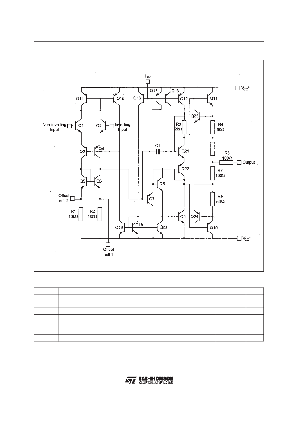
SCHEMATICDIAGRAM
ABSOLUTEMAXIMUMRATINGS
Symbol Parameter UA776M UA776I UA776C Unit
V
V
V
P
T
oper
T
stg
Note : 1. For supply voltages less than±15V, the absolute maximum input voltage is equal to the supply voltage.
2/8
Supply Voltage ±18 V
cc
Differential Input Voltage ±30 V
id
Input Voltage - (note 1) ±15 V
i
Power Dissipation 500 310 310 mW
tot
Output Short-circuit Duration Infinite
Operating Free Air Temperature Range -55 to +125 -40 to +105 0 to +70
Storage Temperature Range -65 to +150 -65 to +150 -65 to +150
o
C
o
C
Page 3
UA776
ELECTRICALCHARACTERISTICS VCC
Symbol Parameter
V
A
SVR Supply Voltage Rejection Ratio(R
I
V
CMR Common-mode Rejection Ratio (R
Input Offset Voltage
I
I
CC
icm
io
io
ib
vd
= +25oC
T
amb
≤ T
T
min.
amb
≤ T
max.
Input Offset Current
= +25oC
T
amb
≤ T
T
min.
amb
≤ T
max.
Input Bias Current
= +25oC UA776M
T
amb
UA776I,C
≤ T
T
min.
amb
≤ T
max.
Large Signal Voltage Gain (VO±10V)
= +25oCR
T
amb
= 75kΩ
R
L
≤ T
T
min.
R
L
T
amb
T
min.
amb
=5kΩ
= +25oC
≤ T
amb
≤ T
≤ T
max.
max.
Supply Current, no load
= +25oC
T
amb
≤ T
T
min.
amb
≤ T
max.
Input Common Mode Voltage Range ±10 ±10 V
= +25oC
T
amb
≤ T
T
min.
amb
≤ T
max.
±15V,T
=5kΩ
L
RL= 75kΩ
≤ 10kΩ)
S
≤ 10kΩ)
S
= +25oC (unless otherwise specified)
amb
I
= 1.5µAI
set
set
Min. Typ. Max. Min. Typ. Max.
25
6
0.7 3
10
2
7.5
2
10
20
10075400
200
400
100
777792 777792
20 25
30
707090 707090
=15µA
25
6
215
40
151550
50
100
160 180
200
Unit
mV
nA
nA
V/mV
dB
µA
dB
I
±V
V
SR Slew Rate (V
K
R
C
R
GBP Gain Bandwidth Product (C
Output Short-circuit Current 0.5 3 15 6 12 30 mA
OS
Output Voltage Swing
OPP
ior
t
r
OV
I
id
o
= +25oCR
T
amb
= 75kΩ
R
L
≤ T
T
min.
amb
≤ T
max.
Offset Voltage Adjustment Range 9 18 mV
= ±10V, CL= 100pF, unity gain)
i
=5kΩ
R
L
= 75kΩ
R
L
Rise Time (Vi= ±20mV, CL= 100pF, unity gain)
=5kΩ
R
L
= 75kΩ
R
L
Overshoot (Vi= ±20mV, CL = 100pF, unity gain)
=5kΩ
R
L
= 75kΩ
R
L
Input Resistance 50 5 MΩ
Differential Input Capacitance 2 2 pF
Output Resistance 5 1 kΩ
= 100pF,T
f = 100kHz R
L
f = 10kHz R
THD Total Harmonic Distortion (f = 1kHz, A
=2VPP,CL= 100pF, T
V
O
=5kΩ
R
L
= 75kΩ
R
L
amb
=25oC)
en Equivalent Input Noise Voltage
(f = 1kHz, R
= 100Ω)4020
s
=5kΩ
L
RL= 75kΩ 121014
0.01 0.1
1.6
=25oC)
amb
=5kΩ
L
= 75kΩ
L
V
= 20dB,
0.3 0.1
0.8
V
101013
V/ms
0.2 0.8
ms
0.35
%
10
0
MHz
0.4 0.7
%
0.025
nV
√Hz
3/8
Page 4

UA776
ELECTRICAL CHARACTERISTICS VCC
Symbol Parameter
V
I
I
A
SVR Supply Voltage Rejection Ratio (R
I
V
CMR Common-mode Rejection Ratio (R
Input Offset Voltage
io
io
ib
vd
CC
icm
= +25oC
T
amb
≤ T
T
min.
amb
≤ T
max.
Input Offset Current
= +25oC
T
amb
≤ T
T
min.
amb
≤ T
max.
Input Bias Current
= +25oC UA776M
T
amb
UA776I,C
≤ T
T
min.
amb
≤ T
max.
Large Signal Voltage Gain(VO±10V)
= +25oCR
T
amb
= 75kΩ
R
L
≤ T
T
min.
R
L
T
amb
T
min.
amb
=5kΩ
= +25oC
≤ T
amb
≤ T
≤ T
max.
max.
Supply Current, no load
= +25oC
T
amb
≤ T
T
min.
amb
≤ T
max.
Input Common Mode Voltage Range ±1 ±1V
= +25oC
T
amb
≤ T
T
min.
amb
≤ T
max.
±3V, T
amb
=5kΩ
L
RL= 75kΩ
≤ 10kΩ)
S
≤ 10kΩ)
S
= +25oC (unlessotherwisespecified)
I
= 1.5µAI
set
Min. Typ. Max. Min. Typ. Max.
25
6
0.7 3
10
2
2
7
10
20
5025200
777792 777792
13 20
25
707090 707090
=15µA
set
25
215
151550
5025200
130 160
Unit
mV
6
nA
40
nA
50
100
V/mV
dB
µA
180
dB
I
±V
V
SR Slew Rate (V
K
R
C
R
GBP Gain Bandwidth Product (C
Output Short-circuit Current 0.5 3 15 2 5 20 mA
OS
Output Voltage Swing
OPP
ior
t
r
OV
I
id
o
= +25oCR
T
amb
=5kΩ
R
L
≤ T
T
min.
R
L
amb
=5kΩ
≤ T
max.
Offset Voltage Adjustment Range 9 18 mV
= ±10V, CL= 100pF, unity gain)
i
=5kΩ
R
L
= 75kΩ
R
L
Rise Time (Vi= ±20mV, CL= 100pF, unity gain)
=5kΩ
R
L
= 75kΩ 3
R
L
Overshoot (Vi= ±20mV, CL = 100pF, unity gain)
=5kΩ
R
L
= 75kΩ 0
R
L
Input Resistance 50 5 MΩ
Differential Input Capacitance 2 2 pF
Output Resistance 5 1 kΩ
= 100pF,T
25
o
C)
L
f = 100kHz R
f = 10kHz R
THD Total Harmonic Distortion (f = 1kHz, A
=2VPP,CL= 100pF, T
V
O
=5kΩ
R
L
= 75kΩ 1
R
L
amb
=25oC)
en Equivalent Input Noise Voltage
(f = 1kHz, R
= 100Ω)2020
s
= 75kΩ
L
RL= 75kΩ
=
amb
=5kΩ
L
= 75kΩ
L
= 20dB,
V
222.4 2
1.9
1.9
0.03
0.075
2.4
V
2.1
2
V/ms
0.35
µs
0.6
%
5
MHz
0.5
%
0.03
nV
√Hz
4/8
Page 5

UA776
5/8
Page 6

UA776
6/8
Page 7

PACKAGE MECHANICAL DATA
8 PINS - PLASTICDIP
UA776
Dim.
A 3.32 0.131
a1 0.51 0.020
B 1.15 1.65 0.045 0.065
b 0.356 0.55 0.014 0.022
b1 0.204 0.304 0.008 0.012
D 10.92 0.430
E 7.95 9.75 0.313 0.384
e 2.54 0.100
e3 7.62 0.300
e4 7.62 0.300
F 6.6 0260
i 5.08 0.200
L 3.18 3.81 0.125 0.150
Z 1.52 0.060
1
Min. Typ. Max. Min. Typ. Max.
Millimeters Inches
7/8
Page 8

UA776
PACKAGE MECHANICAL DATA
8 PINS - PLASTICMICROPACKAGE(SO)
Dim.
Min. Typ. Max. Min. Typ. Max.
Millimeters Inches
A 1.75 0.069
a1 0.1 0.25 0.004 0.010
a2 1.65 0.065
a3 0.65 0.85 0.026 0.033
b 0.35 0.48 0.014 0.019
b1 0.19 0.25 0.007 0.010
C 0.25 0.5 0.010 0.020
c1 45
o
(typ.)
D 4.8 5.0 0.189 0.197
E 5.8 6.2 0.228 0.244
e 1.27 0.050
e3 3.81 0.150
F 3.8 4.0 0.150 0.157
L 0.4 1.27 0.016 0.050
M 0.6 0.024
S8
1
Informationfurnished is believed to be accurate and reliable. However, SGS-THOMSON Microelectronics assumes no responsibility
for the consequences of use ofsuch information nor forany infringement of patents or other rights of third partieswhich may result
from its use.No license isgranted by implication or otherwise under anypatent or patent rightsof SGS-THOMSON Microelectronics.
Specifications mentioned in this publication are subject to change without notice. This publication supersedes and replaces all
informationpreviously supplied. SGS-THOMSON Microelectronics products are not authorized for use as criticalcomponents in life
support devices or systems without express written approval of SGS-THOMSON Microelectronics.
o
(max.)
8/8
1997 SGS-THOMSON Microelectronics – Printed in Italy – All Rights Reserved
SGS-THOMSON Microelectronics GROUP OF COMPANIES
Australia - Brazil - Canada - China - France - Germany - Italy - Japan -Korea - Malaysia - Malta - Morocco
The Netherlands - Singapore - Spain - Sweden - Switzerland- Taiwan - Thailand - United Kingdom- U.S.A.
 Loading...