

Page 1
PRECISION SINGLE OPERATIONALAMPLIFIER
.
INPUTOFFSET VOLTAGE : 3mV max. OVER
TEMPERATURE
.
FREQUENCYCOMPENSATIONWITH A
SINGLE 30pF CAPACITOR(C1)
.
OPERATIONFROM±5V to ±15V
.
LOW POWERCONSUMPTION :
50mW AT±15V
.
CONTINUOUS SHORT-CIRCUIT PROTECTION
.
OPERATIONASACOMPARATORWITH
DIFFERENTIAL INPUTSASHIGHAS±30V
.
NO LATCH-UP WHENCOMMON-MODE
RANGE IS EXCEEDED
.
SAME PIN CONFIGURATION AS THE
LM101A
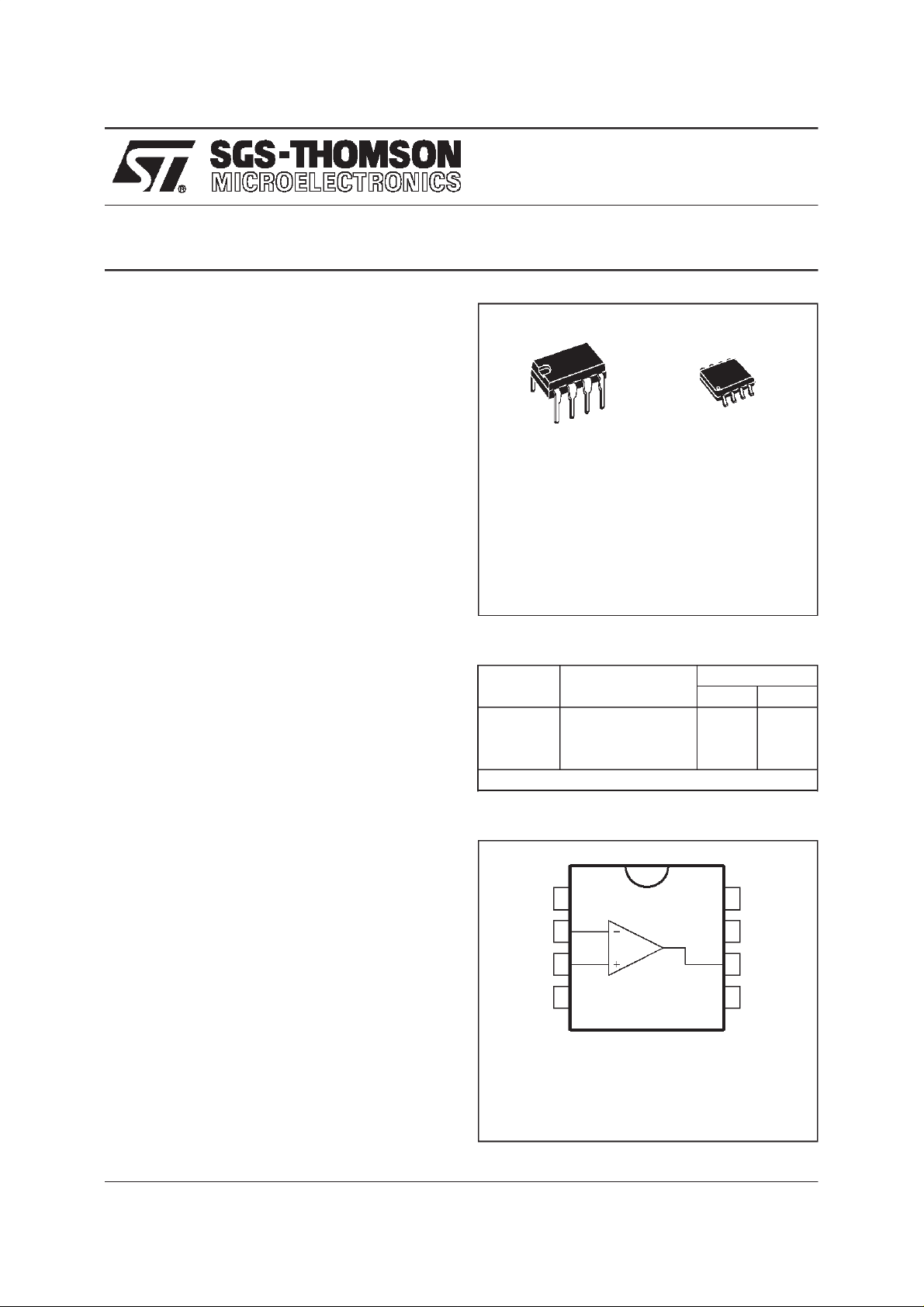
N
DIP8
(Plastic Package)
UA748
D
SO8
(Plastic Micropackage)
DESCRIPTION
The UA748 is a general purpose operational amplifier built on a single silicon chip. The resulting
close match and tight thermal coupling gives low
offsetsand temperaturedrift aswell as fast recovery fromthermaltransients.
.
Short-circuit protection
.
Offsetvoltagenull capability
.
Large common-mode and differential voltage
ranges
.
Low power consumption
.
No latch-up
The unity-gain compensation specified makes the
circuit stablefor all feedbackconfigurations,even
with capacitive loads. However, it is possible to
optimize compensation for best high frequency
performanceatanygain.Thelowpowerdissipation
permits highvoltage operationand simplifiespackaging in full-temperaturerange systems.
ORDER CODES
Part
Number
UA748C 0
UA748I -40
UA748M -55
Example : UA748CN
PIN CONNECTIONS (top view)
1
2
3
4
1 - Offset null 1/ frequency
compensation
2 - Inverting input
3 - Non-inverting input
-
4-V
CC
Temperature
Range
o
C, +70oC ••
o
C, +105oC ••
o
C, +125oC ••
5 - Offset null 2
6 - Output
7-V
8 - Frequency compensation
Package
ND
+
CC
8
7
6
5
December 1997
1/8
Page 2
UA748
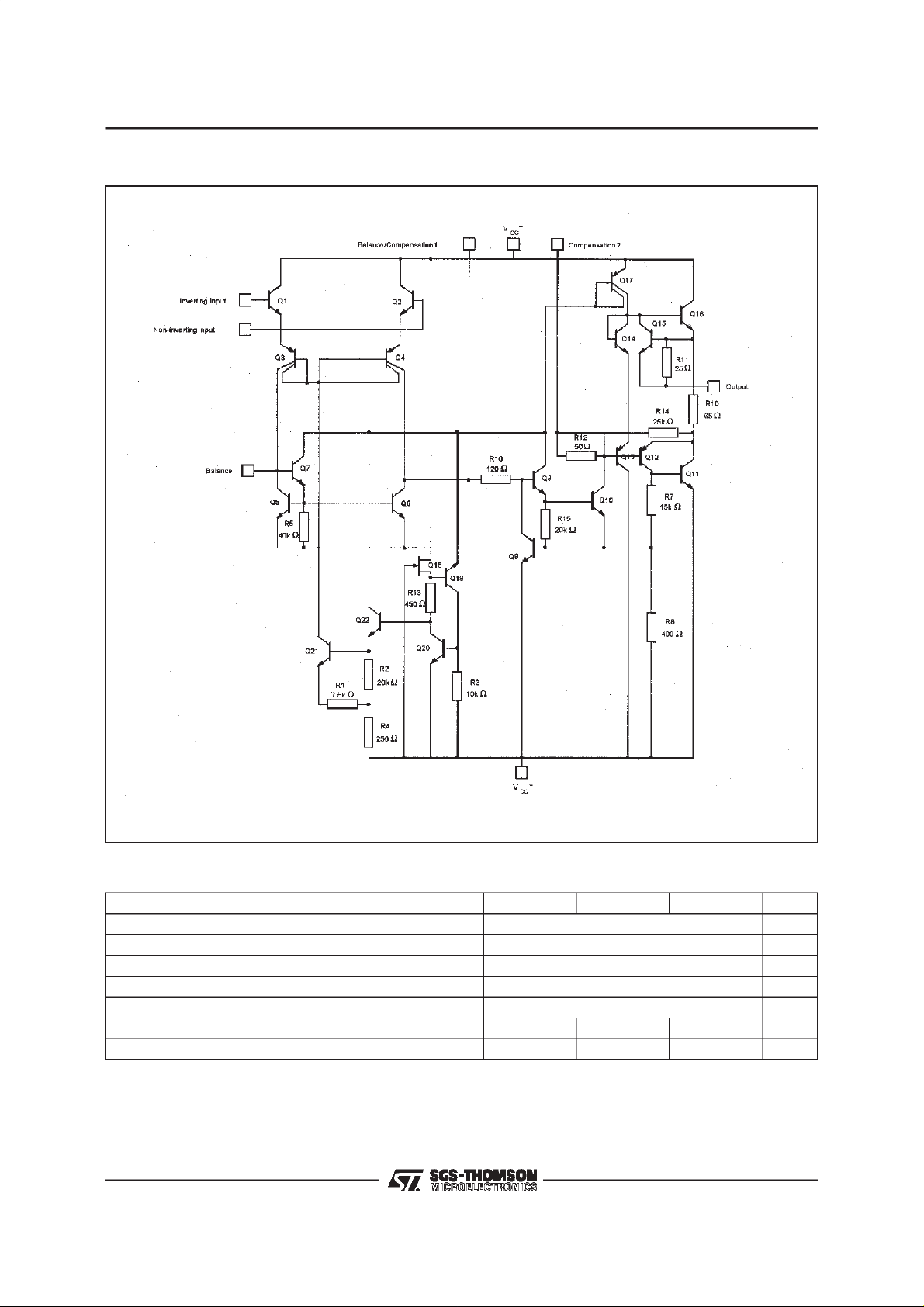
SCHEMATICDIAGRAM
ABSOLUTEMAXIMUMRATINGS
Symbol Parameter UA748M UA748I UA748C Unit
Supply Voltage ±22 V
cc
Differential Input Voltage ±30 V
id
Input Voltage ±15 V
i
Power Dissipation 500 mW
tot
Output Short-circuitDuration Infinite
Operating Free Air Temperature Range -55 to +125 -40 to +105 0 to +70
Storage Temperature Range -65 to +150 -65 to +150 -65 to +150
2/8
V
V
V
P
T
oper
T
stg
o
C
o
C
Page 3

ELECTRICALCHARACTERISTICS
≤ VCC
±5V
Symbol Parameter
V
io
I
io
I
ib
A
vd
SVR Supply Voltage Rejection Ratio (R
I
CC
V
icm
CMR Common-mode Rejection Ratio(R
≤±20V,C1 = 30pF, T
amb
Input OffsetVoltage (RS≤ 10kΩ)
= +25oC
T
amb
≤ T
T
min.
amb
≤ T
max.
Input OffsetCurrent
= +25oC
T
amb
≤ T
T
min.
amb
≤ T
max.
Input Bias Current
= +25oC
T
amb
≤ T
T
min.
amb
≤ T
max.
Large Signal VoltageGain *
= ±15V, VO±10V, RL=2kΩ)
(V
CC
= +25oC
T
amb
≤ T
T
min.
T
amb
T
min.
amb
= +25oC
≤ T
amb
≤ T
≤ T
max.
max.
Supply Current, no load
= +25oC
T
amb
≤ T
T
min.
amb
≤ T
max.
Input Common Mode Voltage Range (VCC=
±20V)
= +25oC
T
amb
≤ T
T
min.
T
amb
T
min.
amb
= +25oC
≤ T
amb
≤ T
≤ T
max.
max.
= +25oC (unlessotherwise specified)
UA748I/M UA748C
Min. Typ. Max. Min. Typ. Max.
≤ 10kΩ)
S
≤ 10kΩ)
S
0.2 2
25 75
1.5 10
5025100 251510
808096 707096
1.8 3
±15
±15
808096 707096
3
10
20
3
UA748
Unit
mV
2 7.5
10
nA
70 250
300
nA
250
70
V/mV
dB
mA
1.8 3
3
V
±15
±15
dB
I
±V
Output Short-circuit Current (VCC= ±15V) 10 30 50 10 30 50 mA
OS
Output Voltage Swing (VCC= ±15V)
OPP
= +25oCR
T
amb
=2kΩ
R
L
≤ T
T
min.
R
L
amb
=2kΩ
≤ T
max.
SR Slew Rate
= ±10V,RL=2kΩ,CL= 100pF, unity gain) 0.25 0.5 0.25 0.5
(V
i
t
Rise Time
r
K
OV
Z
I
R
o
= ±20mV, RL=2kΩ,CL= 100pF,unity gain) 0.3 0.3
(V
i
Overshoot
= 20mV, RL=2kΩ, CL =100pF, unity gain) 5 5
(V
i
Input Impedance (VCC= ±15V) 1.5 4 1.5 4 MΩ
Output Resistance (VCC= ±15V) 75 75 Ω
GBP Gain Bandwidth Product
= 10mV, RL=2kΩ,CL= 100pF,f = 100kHz) 0.5 1 0.5 1
(V
i
THD Total Harmonic Distortion
DV
DI
(f = 1kHz, A
100pF)
Input OffsetCurrent Drift
io
io
o
C ≤ T
25
T
min.
Input OffsetVoltage Drift
T
min.
= 20dB, RL=2kΩ,VO=2VPP,CL=
V
≤ T
amb
amb
amb
≤ T
≤ T
max.
max.
max.
≤ T
≤ T
= 10kΩ
L
RL= 10kΩ
12
14
10
13
12
10
0.015 0.015
1020100
200
315 630
12
10
12
10
14
13
1020300
600
V/µs
µs
%
MHz
%
pA/
µV/
V
o
C
o
C
3/8
Page 4

UA748
4/8
Page 5

UA748
5/8
Page 6

UA748
6/8
Page 7

PACKAGE MECHANICAL DATA
8 PINS- PLASTIC DIP
UA748
Dim.
A 3.32 0.131
a1 0.51 0.020
B 1.15 1.65 0.045 0.065
b 0.356 0.55 0.014 0.022
b1 0.204 0.304 0.008 0.012
D 10.92 0.430
E 7.95 9.75 0.313 0.384
e 2.54 0.100
e3 7.62 0.300
e4 7.62 0.300
F 6.6 0260
i 5.08 0.200
L 3.18 3.81 0.125 0.150
Z 1.52 0.060
Min. Typ. Max. Min. Typ. Max.
Millimeters Inches
7/8
Page 8

UA748
PACKAGE MECHANICAL DATA
8 PINS- PLASTIC MICROPACKAGE (SO)
Dim.
Min. Typ. Max. Min. Typ. Max.
Millimeters Inches
A 1.75 0.069
a1 0.1 0.25 0.004 0.010
a2 1.65 0.065
a3 0.65 0.85 0.026 0.033
b 0.35 0.48 0.014 0.019
b1 0.19 0.25 0.007 0.010
C 0.25 0.5 0.010 0.020
c1 45
o
(typ.)
D 4.8 5.0 0.189 0.197
E 5.8 6.2 0.228 0.244
e 1.27 0.050
e3 3.81 0.150
F 3.8 4.0 0.150 0.157
L 0.4 1.27 0.016 0.050
M 0.6 0.024
S8
Informationfurnished is believedto be accurate andreliable. However,SGS-THOMSON Microelectronics assumes no responsibility
for the consequences ofuse of such information nor forany infringement of patents or otherrights of third partieswhich may result
from its use. No license isgranted byimplication or otherwise under anypatent or patent rights ofSGS-THOMSON Microelectronics.
Specifications mentioned in this publication are subject to change without notice. This publication supersedes and replaces all
informationpreviously supplied. SGS-THOMSON Microelectronics products are not authorized foruse as criticalcomponents in life
support devices or systems without express written approvalof SGS-THOMSON Microelectronics.
o
(max.)
8/8
1997 SGS-THOMSON Microelectronics – Printed in Italy– All Rights Reserved
SGS-THOMSON Microelectronics GROUP OF COMPANIES
Australia - Brazil - Canada - China - France - Germany - Italy- Japan - Korea - Malaysia - Malta - Morocco
The Netherlands - Singapore - Spain - Sweden - Switzerland - Taiwan - Thailand - United Kingdom- U.S.A.
 Loading...