

Page 1
TELEFUNKEN Semiconductors
U 210 B / U 210 B–FP
Phase Control Circuit – Load Current Feedback Applications
Technology: Bipolar
Features
Externally controlled integrated amplifier
Variable soft start
Automatic retriggering
Voltage and current synchronisation
Case: DIP 14, SO 16
Triggering pulse typ. 125 mA
Internal supply voltage monitoring
Temperature constant reference source
Current requirement ≤ 3 mA
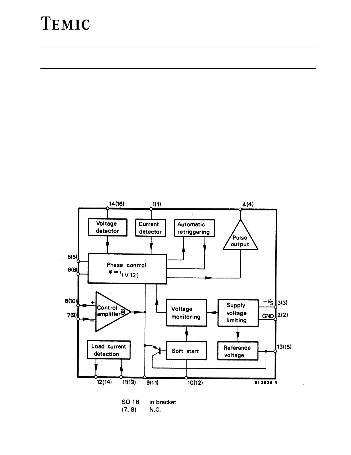
Figure 1 Block diagram
Preliminary Information
1
Page 2
U 210 B / U 210 B–FP
TELEFUNKEN Semiconductors
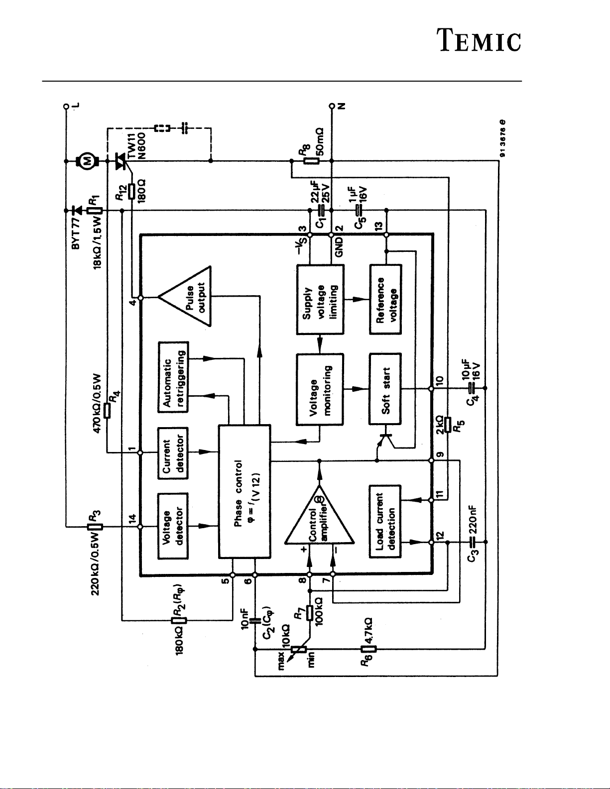
Figure 2 Block diagram with external circuitry
Open loop control with load current compensation
2
Preliminary Information
Page 3

TELEFUNKEN Semiconductors
U 210 B / U 210 B–FP
Description
Mains supply
The U 210 B is fitted with voltage limiting and can therefore be supplied directly from the mains. The supply voltage
and R
between Pin 2 (+pol/) and Pin 3 builds up across D
1
can be approximated using:
VM–V
2 I
S
S
R1=
Further information regarding the design of the mains supply can be found in the data sheets in the appendix. The reference
voltage source on Pin 13 of typ. –8.9 V is derived from the supply voltage. It represents the reference level of the control
unit. Operating using an externally stabiIised DC voltage is not recommended.
If the supply cannot be taken directly from the mains because the power dissipation in R
circuit shown in the following Figure 3 should be employed.
and is smoothed by C1. The vaIue of the series resistance
1
would be too large, then the
1
Figure 3 Supply voltage for high current requirements
Phase control
The function of the phase control is largely identical to that of the well known components U 111 B and TEA 1007. The
phase angle of the trigger pulse is derived by comparing the ramp voltage, which is mains synchronised by the voltage
detector, with the set value on the control input Pin 9. The slope of the ramp is determined by C
The charging current can be varied using R
on Pin 5. The maximum phase angle
2
can also be adjusted using R2.
max
and its charging current.
2
When the potential on Pin 6 reaches the nominal value predetermined at Pin 9, then a trigger pulse is generated whose
width t
is determined by the value of C
p
(the value of C
2
and hence the pulse width can be evaluated by assuming 8 s/nF).
2
At the same time, a latch is set, so that as long as the automatic retriggering has not been activated, then no more pulses
can be generated in that half cycle.
The current sensor on Pin 1 ensures that, for operation with inductive loads, no pulse will be generated in a new half cycle
as long as current from the previous half cycle is still flowing in the opposite direction to the supply voltage at that instant.
This makes sure that ”Gaps” in the load current are prevented.
The control signal on Pin 9 can be in the range 0 V to –7 V (reference point Pin 2).
If V
pin9
angle
= –7 V then the phase angle is at maximum =
is when V
min
pin9
= V
pin2
.
i .e. the current flow angle is a minimum. The minimum phase
max
Voltage monitoring
As the voltage is built up, uncontrolled output pulses are avoided by internal voltage surveillance. At the same time, all
of the latches in the circuit (phase control, soft start) are reset and the soft–start capacitor is short circuited. Used with
a switching hysteresis of 300 mV, this system guarantees defined start–up behaviour each time the supply voltage is
switched on or after short interruptions of the mains supply.
Preliminary Information
3
Page 4
U 210 B / U 210 B–FP
TELEFUNKEN Semiconductors
Soft–start
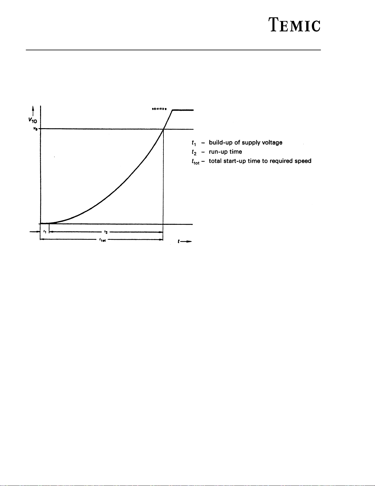
As soon as the supply voltage builds up (t1), the integrated soft–start is initiated. The figure below shows the behaviour
of the voltage across the soft–start capacitor and is identical with the voltage on the phase control input on Pin 9. This
behaviour allows a gentle start–up for the motor.
Figure 4 Soft–start
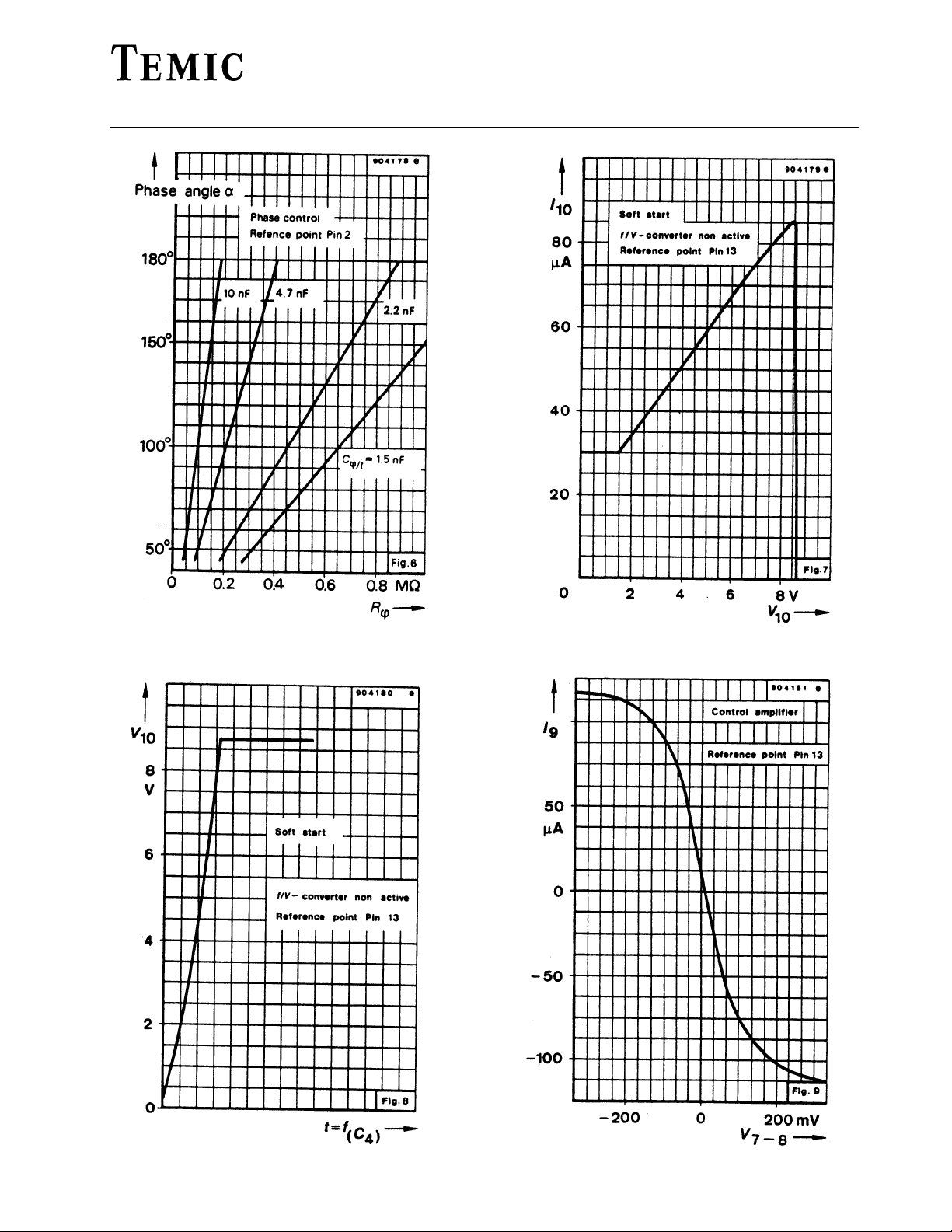
is first charged with typ. 30 A. The charging current then increases as the voltage across C
C
3
progressively rising charging function with more and more strongly accelerates the motor with increasing rotational
speed. The charging function determines the acceleration up to the set point. The charging current can have a maximum
value of 85 A.
increases giving a
4
Control amplifier
The integrated control amplifier with differential input has a bipolar current output, with typically ±110 A at Pin 9 and
a transmittance of typ. 1000 A/V. The amplification and frequency response are determined by external circuit. For
operation as a power control, it should be connected with Pin 7. Phase angle of the firing pulse can be adjusted by using
the voltage at Pin 8. An internal limiting circuit prevents the voltage on Pin 9 becoming more negative than V
13
+ 1 V.
Load current detection, Figure 2
Voltage drop across R8, dependent of load current, generates an input–current at Pin 11 limited by R5. Proportional output
current of 0.44 x I
Capacitor C
proportionality , can be used according to the application i.e., load current compensation or load current regulation.
3
(CTR) is available at Pin 12. It is proportional with respect to phase and amplitude of load current.
11
integrates the current whereas resistor R
evaluates it. The voltage obtained due to load current
7
Pulse output stage
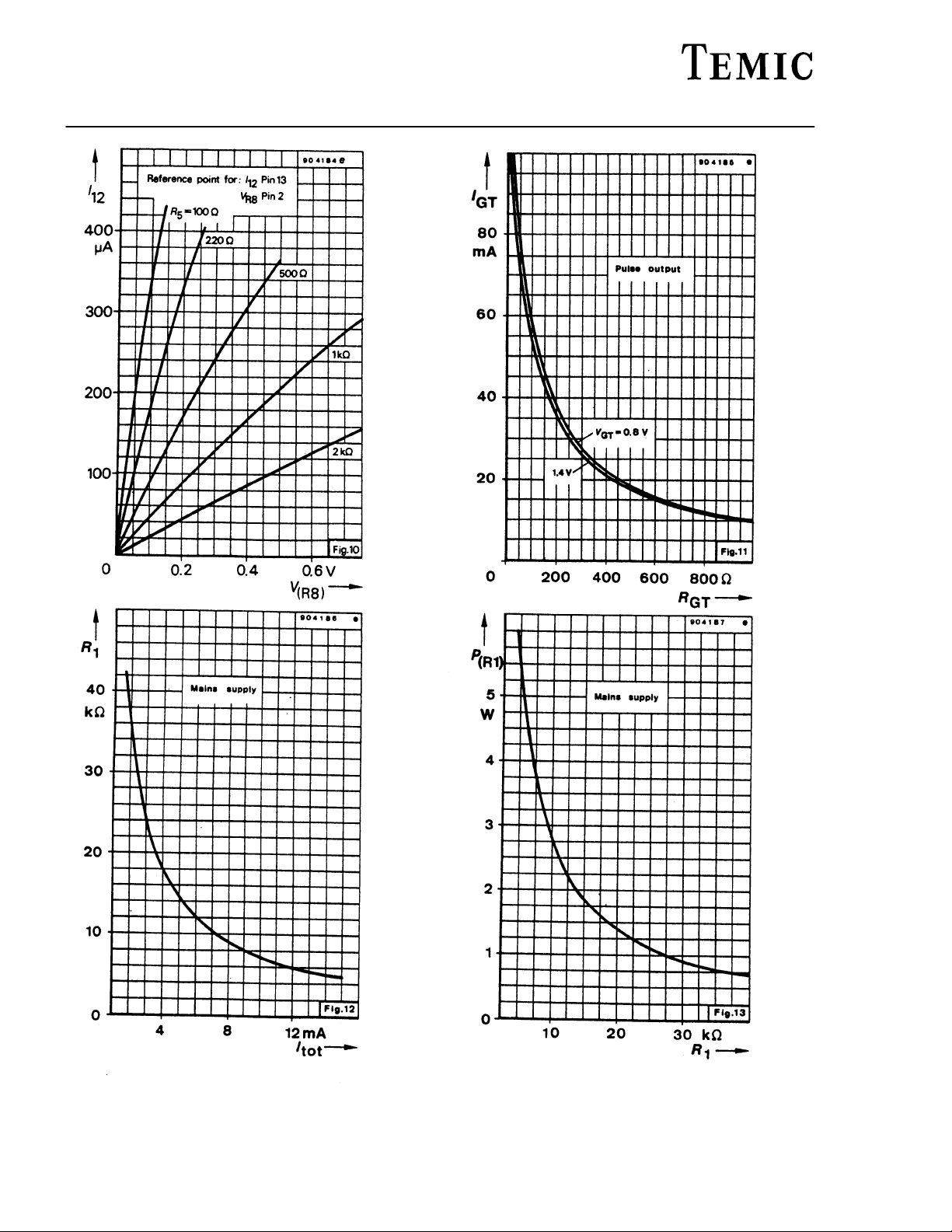
The pulse output stage is short circuit protected and can typically deliver currents of 125 mA. For the design of smaller
triggering currents, the function I
and the TEA 1007, the pulse output stage of the U 210 B has no gate bypass resistor.
= f (RGT) has been given in the data sheets in the appendix. In contrast to the U 11 1 B
GT
Automatic retriggering
The automatic retriggering prevents half cycles without current flow, even if the triac is turned off earlier e.g. due to not
exactly centred collector (brush lifter) or in the event of unsuccessful triggering. After a time lapse of t
generated another triggering pulse which is repeated until either the triac fires or the half cycle finishes.
4
Preliminary Information
=4.5 tp is
pp
Page 5
TELEFUNKEN Semiconductors
U 210 B / U 210 B–FP
General hints and explanation of terms
To ensure safe and trouble–free operation, the following points should be taken into consideration when circuits are being
constructed or in the design of printed boards.
The connecting lines from C
be as short as possible, and the connection to Pin 2
should not carry any additional high current such as the
to Pin 6 and Pin 2 should
2
load current. When selecting C
coefficient is desirable.
, a low temperature
2
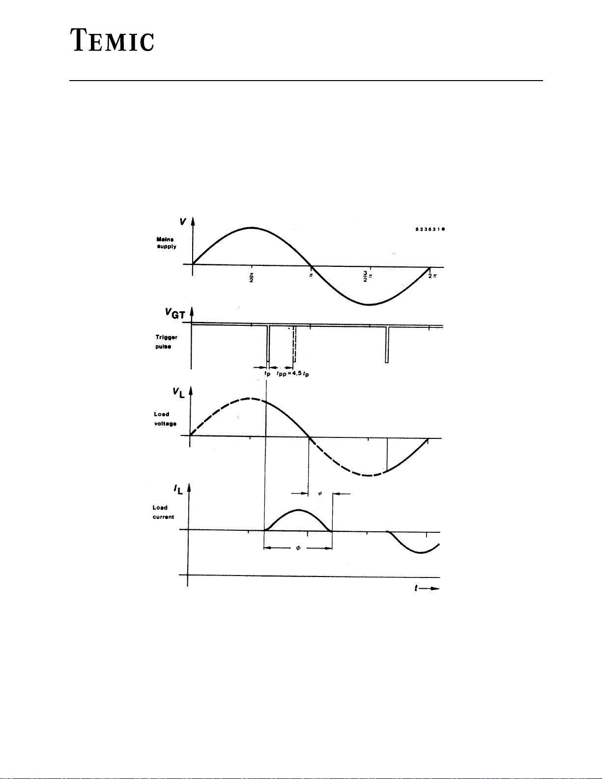
Figure 5 Explanation of terms in phase relationship
Preliminary Information
5
Page 6
U 210 B / U 210 B–FP
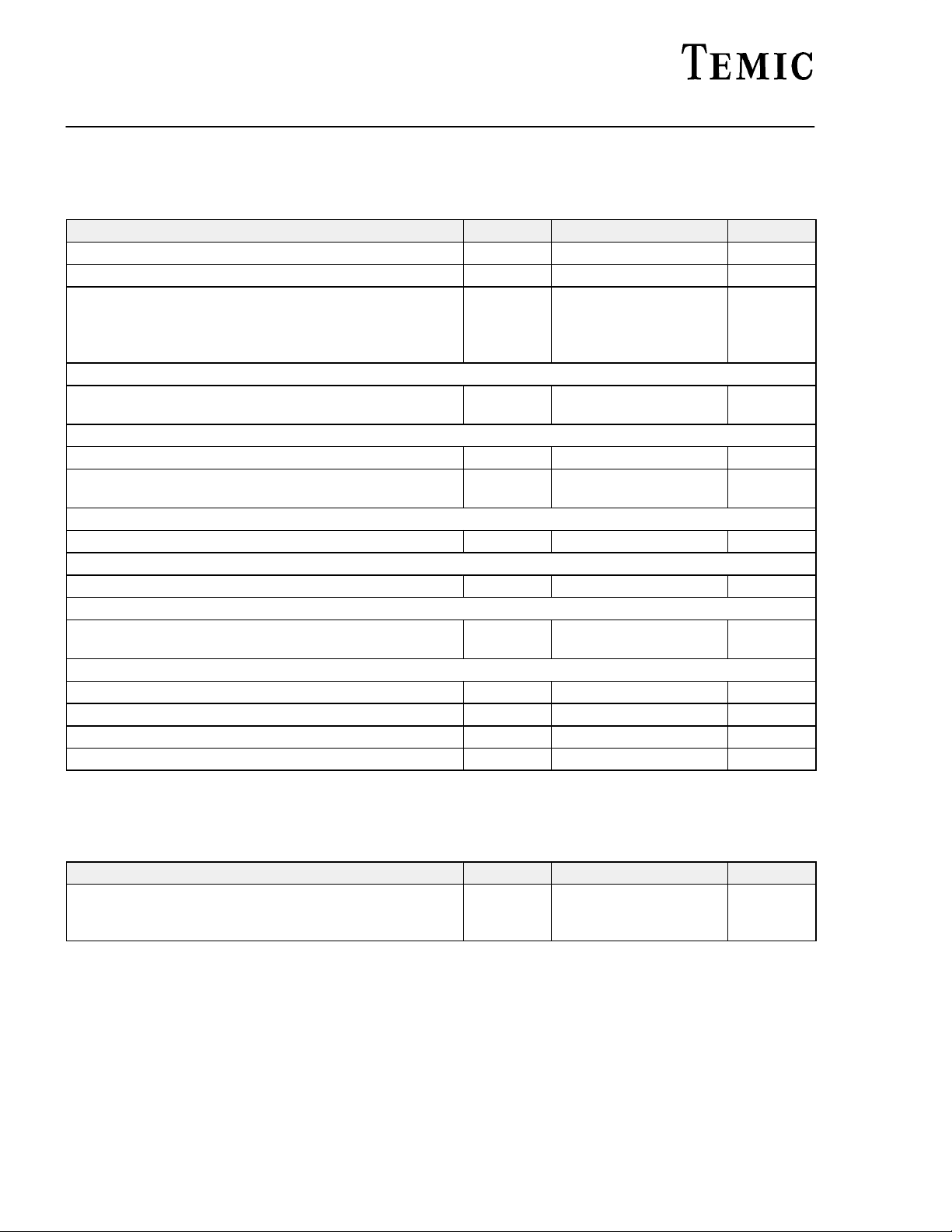
Absolute Maximum Ratings
Reference point Pin 2, unless otherwise specified
Parameters Symbol Value Unit
Current requirement Pin 3 –I
Peak current requirement t ≤ 10 s Pin 3 –i
Synchronisation current Pin 1
Pin 14
t ≤ 10 s Pin 1
t ≤ 10 s Pin 14
Load current monitoring
Input current Pin 11
t ≤ 10 s Pin 11
Phase control
Input voltage Pin 9 –V
Input current Pin 9
Pin 5
Soft–start
Input voltage Pin 10 –V
Pulse output
Reverse voltage Pin 4 V
Amplifier
Input voltage Pin 8
Pin 7
Reference voltage source
Output current Pin 13 I
Storage temperature range T
Junction temperature T
Ambient temperature range T
–I
–I
S
s
sync.I
sync.V
–i
I
"i
v
–I
I
–I
I
"I
–I
I
o
V
I
–V
o
stg
j
amb
TELEFUNKEN Semiconductors
30 mA
100 mA
5
5
35
35
2
5
I
I
0 ... 7 V
500
1
I
V13 ... 0 V
VS ... 5 V
0 ... V
S
I
V13 ... 0 V
7.5 mA
–40 ... +125 °C
125 °C
–10 ... +100 °C
mA
mA
mA
mA
mA
mA
A
mA
Thermal Resistance
Parameters Symbol Maximum Unit
Junction ambient DIP 14
SO 16 on p.c.
SO 16 on ceramic
6
Preliminary Information
R
R
R
thJA
thJA
thJA
120
180
100
K/W
K/W
K/W
Page 7

TELEFUNKEN Semiconductors
Electrical Characteristics
U 210 B / U 210 B–FP
–Vs = 13.0 V, T
= 25 °C, reference point Pin 2, unless otherwise specified
amb
Parameters Test Conditions / Pin Symbol Min Typ Max Unit
Supply voltage for mains
Pin 3 –V
operations
Supply voltage limitation –IS = 3 mA Pin 3
–I
= 30 mA Pin 3
S
DC supply current –VS =13.0 V Pin 3 –I
Reference voltage source –IL = 10 mA Pin 13
–I
= 5 mA Pin 13
L
Temperature coefficient Pin 13 –TC
Voltage monitoring
Turn–on threshold Pin 3 –V
Turn–off threshold Pin 3 –V
Phase control currents
Current synchronisation Pin 1 I
Voltage synchronisation Pin 14 I
Voltage limitation ±IL= 5 mA Pin 1
Pin 14
Reference ramp
Load current, Figure 6 I6 = f(Rf)
R
= 1 K ... 820 KW Pin 6 I
f
Rö–reference voltage a ≥ 180 ° Pin5,3 V
Temperature coefficient Pin 5 TC
Pulse output, Figure 12
Output pulse current RGT= 0, VGT=1.2 V Pin 4 I
Reverse current Pin 4 I
Output pulse width
Cö = 10 nF Pin4,2 t
Automatic retriggering
Repetition rate Pin 4 t
Amplifier
Common mode voltage
Pin7,8 V
range
Input bias current Pin 8 I
Input offset voltage Pin7,8 V
Output current, Figure 9 Pin 9
Pin 9
Short circuit forward trans-
I
12
= f(V
) Pin 9 Y
10-11
mittance
–V
–V
–V
–V
SON
SOFF
sync.I
sync.V
"V
"V
ö
VöRef
or
p
pp
7,8
IB
IO
–I
+I
S
S
S
S
Ref
Ref
VRef
I
I
6
Ref
o
O
O
f
13.0 V
14.6
14.7
Limit
16.6
16.8
V
V
V
1.2 2.5 3.0 mA
8.6
8.3
8.9 9.2
9.1
V
V
0.5 mV/K
11.2 13.0 V
9.9 10.9 V
0.35 3.5 mA
0.35 3.5 mA
8.0
8.0
8.9
8.9
9.5
9.5
V
V
1 20 mA
1.06 1.13 1.18 V
0.5 mV/K
100 125 150 mA
0.01 3.0 mA
80 ms
3 4.5 6 t
V
13
–1 V
p
0.01 1 mA
10 mV
75
88
110
120
145
165
mA
mA
1000 mA/V
Preliminary Information
7
Page 8
U 210 B / U 210 B–FP
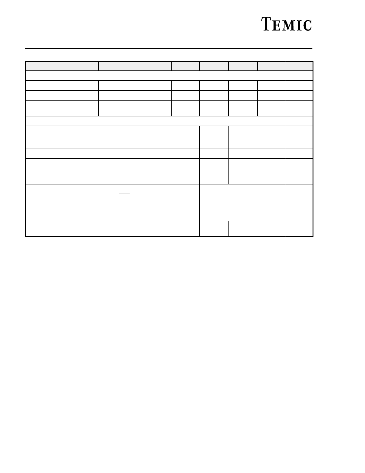
Parameters Test Conditions / Pin Symbol Min Typ Max Unit
Soft-start, Figures 7, 8
Starting current V10 = V
13
Final current V10 = –0.5 V Pin 10 I
Discharge current, restart
pulse
Load current detection, Figure 11
Input current voltage VI = 300 mV, RV = 1 K
Input offset voltage Pin 11 V
Output open current VI = 0 V, RV= 1 K Pin 12 I
Output current VI = 300 mV, RV = 1 K
V
= V
12
13
Current transfer ratio
CTR =
I
I
= 150 A
12
= 300 A
12
I
12
I
11
Temperature coefficient of
current transfer ratio
Pin 10 I
Pin 10 –I
Pin 11
Pin 11
Pin 12 I
Pin 12/11
Pin 12/11
Pin 12/11 TC 0.2
o
O
O
I
I
I
I
IO
O
O
CTR
CTR
TELEFUNKEN Semiconductors
20 30 50 A
50 85 130 A
0.5 3 10 mA
0
300
–8 0 mV
1 4 A
120 127 134 A
0.44 ± 5%
0.42 ± 6%
500
308
A
A
0
/00/K
8
Preliminary Information
Page 9
TELEFUNKEN Semiconductors
U 210 B / U 210 B–FP
Preliminary Information
9
Page 10
U 210 B / U 210 B–FP
TELEFUNKEN Semiconductors
10
Preliminary Information
Page 11
TELEFUNKEN Semiconductors
Design calculations
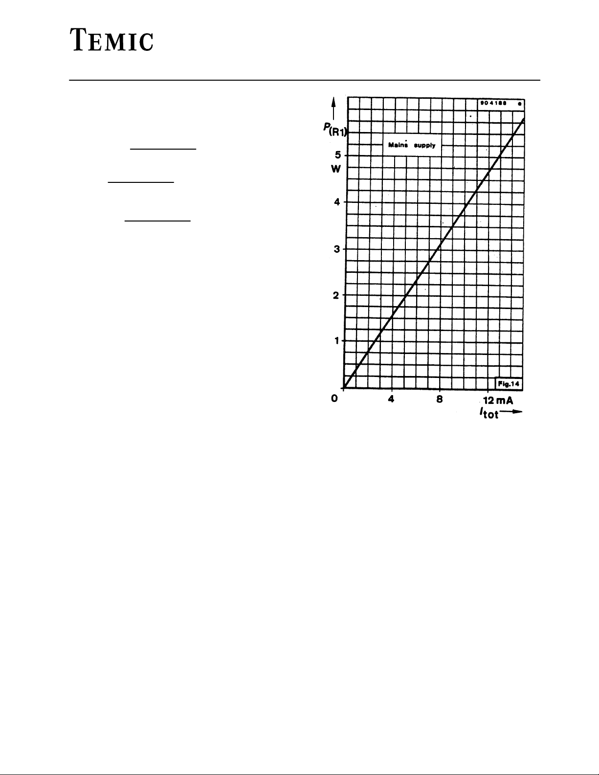
The following equations can be used for the evaluation
of the series resistor R
V
R
= 0.9 @
1max
V
Mmax
=
R
1min
2 I
for worst case conditions:
1
– V
Mmin
– V
Smax
2 I
Smax
tot
Smin
U 210 B / U 210 B–FP
P (R
1max
) =
(V
Mmax
2 R
– V
1
Smin)
2
where:
V
= Mains voltage 220 V
M
Vs = Supply voltage on Pin 4
I
= T otal DC current requirement of the circuit
tot
I
Smax
I
p
I
x
R
can be easily evaluated from Figures 12 – 14
1
Smax
+ Ip + I
x
= I
= Current requirement of the IC in mA
= Average current requirement of the triggering pulses
= Current requirement of other peripheral components
Preliminary Information
11
Page 12
U 210 B / U 210 B–FP
TELEFUNKEN Semiconductors
Applications
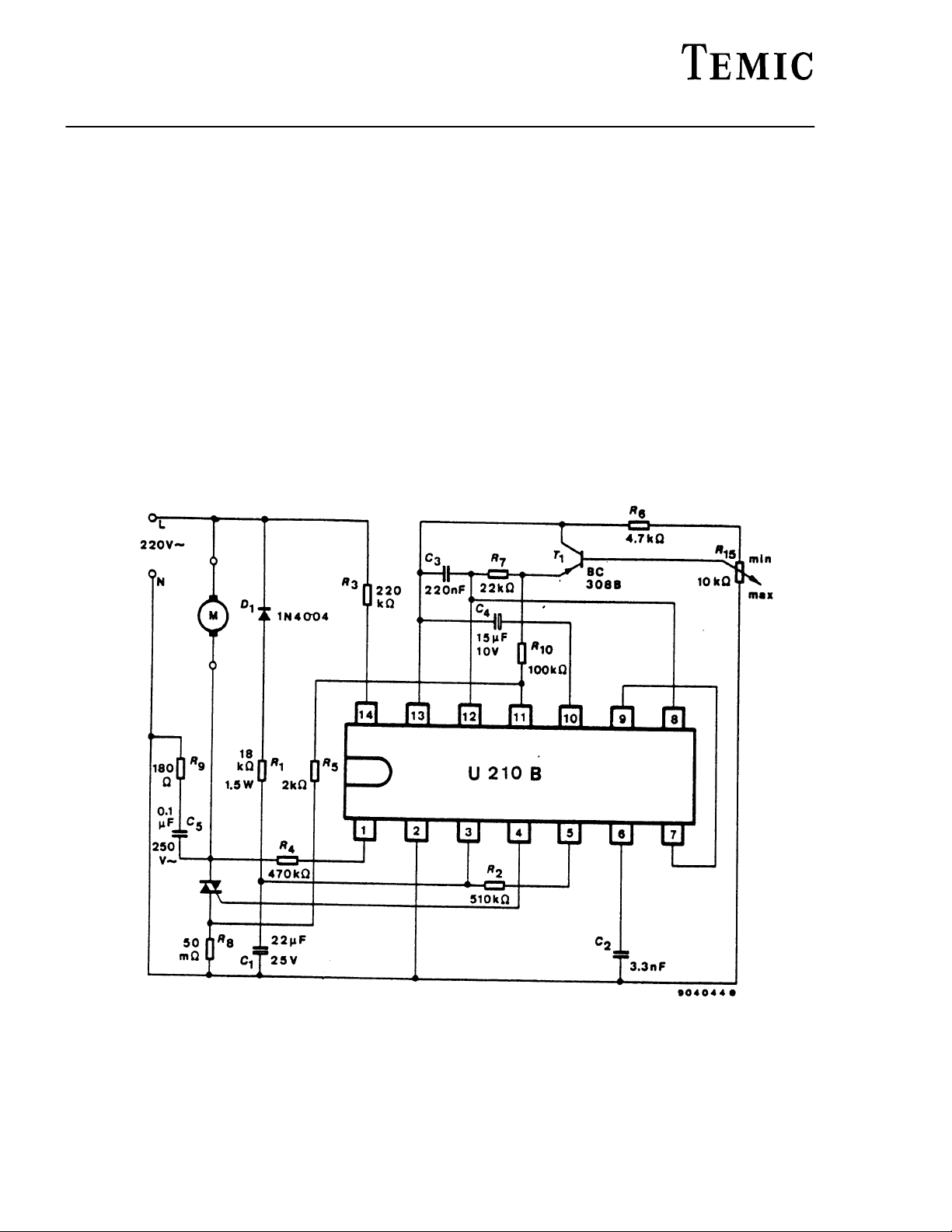
In contrast to simple speed controller”, the circuits shown in Figures 15 and 16, react to the load dependent speed drop
in which the magnitude of the load current acts on the speed compensation.
For this purpose, the load current is measured by shunt resistor R8. The voltage drop generates a current at Pin 11
dependent of R
Rated impedance of the output current at Pin 12 is represented through the coupling resistance R
of the set point.
, which reflects in the specified current at the output of Pin 12.
5
and the total impedance
7
The integrated load current proportional signal at C
by the increase of load current follows an automatic increase of manipulated set point, so that a compensation of speed
falls.
Compensation arrangement is influenced with resistance values i.e. R
whereas the higher effect is achieved by increasing the value of R
increased up to the value where the drive system (motor) starts to oscillate.
Dimensioning in the applications are with the drill machine of 700 W power.
effects in the same direction on the control input as the set point i.e.,
3
(= 100 ... 5 k) and R7 (= 10 k ... 150 k)
5
and decreasing R5. Influence of compensation can be
7
12
Figure 15 Speed control with load current compensation
Preliminary Information
Page 13
TELEFUNKEN Semiconductors
U 210 B / U 210 B–FP
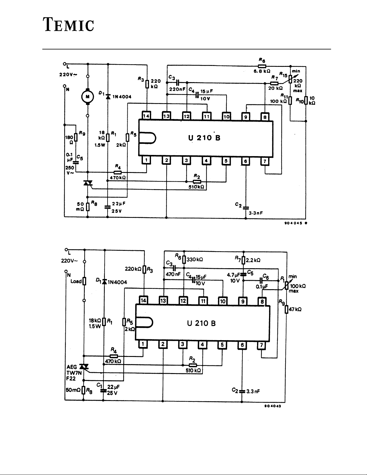
Figure 16 Speed control with load current compensation
Figure 17 Load current regulation with soft start
Current regulation is achieved by the integrated operational amplifier as PI–controller (R
of the operational amplifier is directly connected at C
Desired value is obtained with the help of potentiometer at Pin 8.
with load current proportional test signal (actual value).
3
Preliminary Information
, C5, C6). Inverted input (Pin 7)
7
13
Page 14
U 210 B / U 210 B–FP
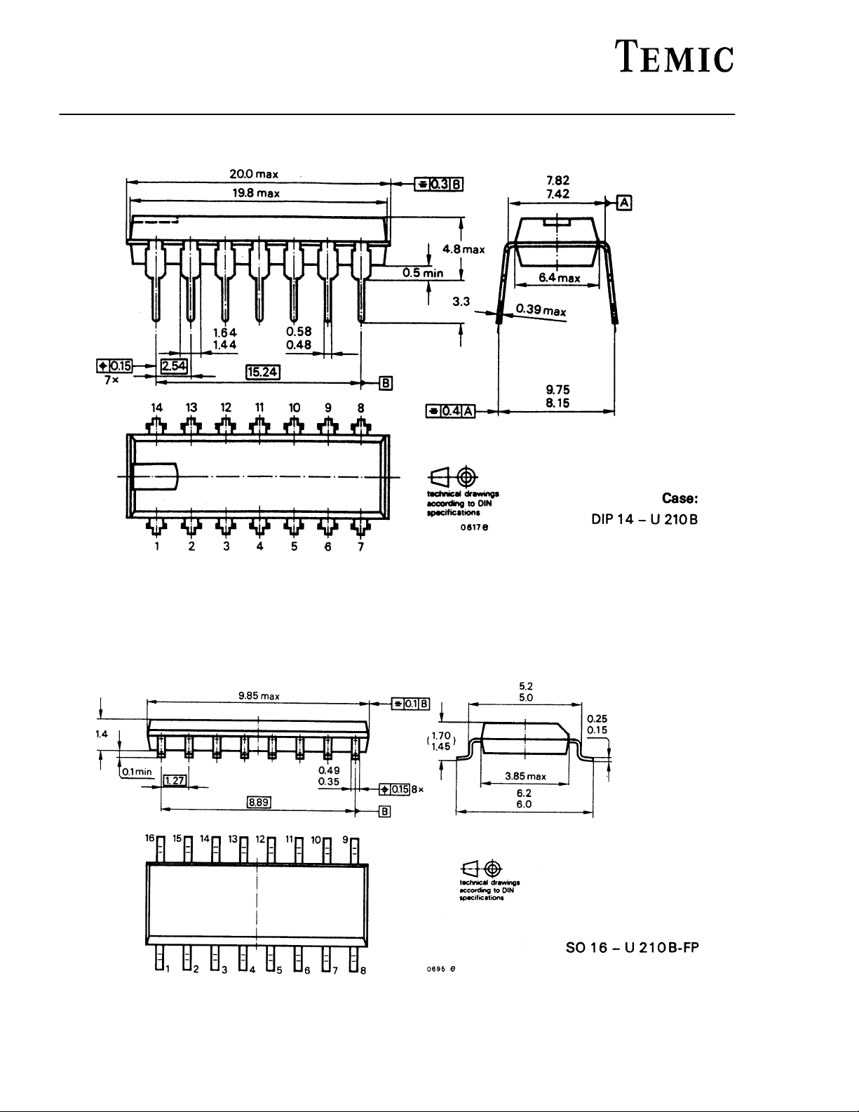
Dimensions in mm
TELEFUNKEN Semiconductors
14
Preliminary Information
Page 15

TELEFUNKEN Semiconductors
U 210 B / U 210 B–FP
OZONE DEPLETING SUBSTANCES POLICY STATEMENT
It is the policy of TEMIC TELEFUNKEN microelectronic GmbH to
1. Meet all present and future national and international statutory requirements and
2. Regularly and continuously improve the performance of our products, processes, distribution and operating systems
with respect to their impact on the health and safety of our employees and the public, as well as their impact on the
environment.
Of particular concern is the control or elimination of releases into the atmosphere of those substances which are known
as ozone depleting substances (ODSs).
The Montreal Protocol (1987) and its London Amendments (1990) will soon severely restrict the use of ODSs and forbid
their use within the next ten years. Various national and international initiatives are pressing for an earlier ban on these
substances.
TEMIC TELEFUNKEN microelectronic GmbH semiconductor division has been able to use its policy of continuous
improvements to eliminate the use of any ODSs listed in the following documents.
1. Annex A, B and list of transitional substances of the Montreal Protocol and the London Amendments respectively
2. Class I and II ozone depleting substances in the Clean Air Act Amendments of 1990 by the Environmental Protection
Agency (EPA) in the USA and
3. Council Decision 88/540/EEC and 91/690/EEC Annex A, B and C (transitional substances) respectively.
TEMIC can certify that our semiconductors are not manufactured with and do not contain ozone depleting substances.
We reserve the right to make changes without further notice to improve technical design.
Parameters can vary in different applications. All operating parameters must be validated for each customer
application by customer. Should Buyer use TEMIC products for any unintended or unauthorized application, Buyer
shall indemnify TEMIC against all claims, costs, damages, and expenses, arising out of, directly or indirectly, any
claim of personal damage, injury or death associated with such unintended or unauthorized use.
TEMIC TELEFUNKEN microelectronic GmbH, P.O.B. 3535, D-74025 Heilbronn, Germany
Telephone: 49 (0)7131 67 2831, Fax Number: 49 (0)7131 67 2423
Preliminary Information
15
 Loading...