

Datasheet TYN816RG, TYN816, TYN1016RG, TYN1016, TYN616RG Datasheet (SGS Thomson Microelectronics)
...Page 1
®
TN16 and TYNx16 Series
STANDARD 16A SCRs
MAIN FEATURES:
A
Symbol Value Unit
I
T(RMS)
V
DRM/VRRM
I
GT
16 A
600 to 1000 V
25 mA
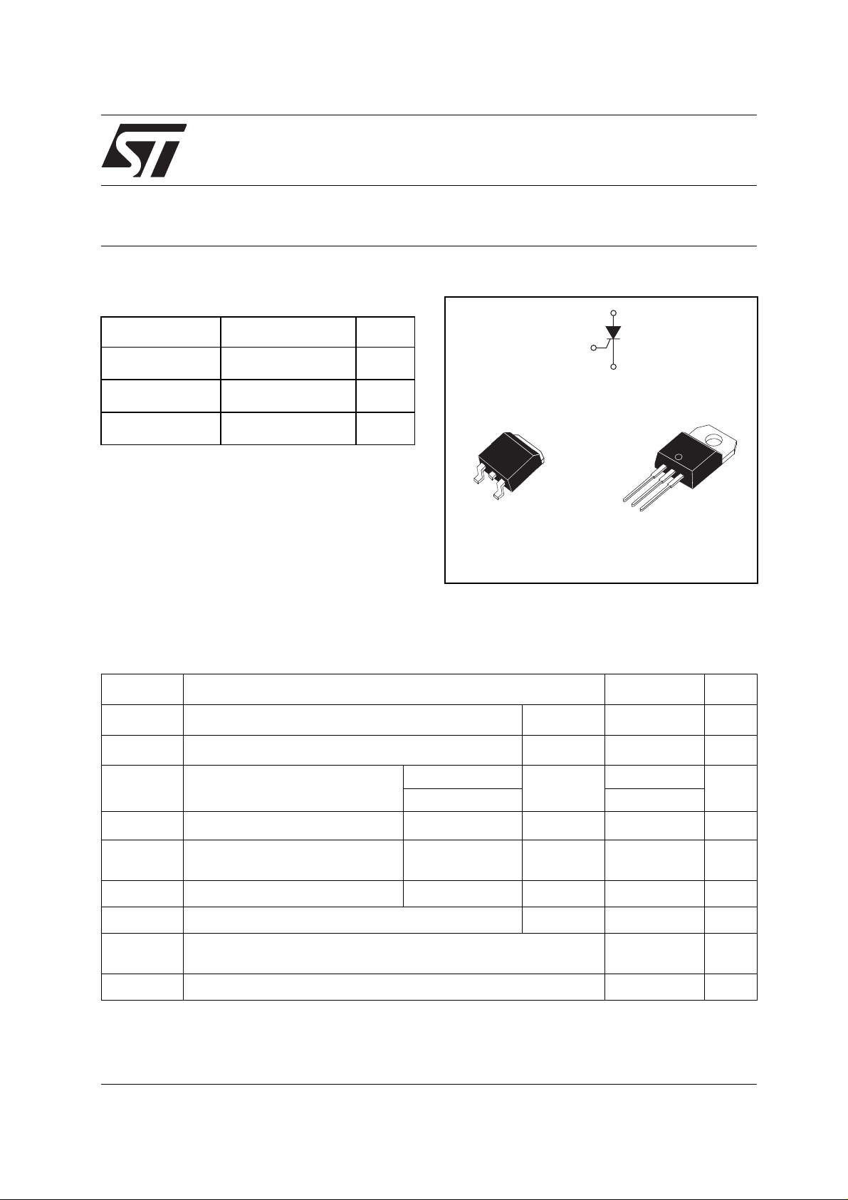
DESCRIPTION
The TYN / TN16 SCR Series is suitable for
general purpose applications.
Using clip assembly technology, they provide a
K
A
G
D2PAK
(TN16-G)
A
G
K
K
A
G
TO-220AB
(TYN)
superior performance in surge current capabilities.
ABSOLUTE RATINGS (lim iting values)
Symbol Parameter Value Unit
A
I
T(RMS)
T
(AV)
I
TSM
²
I
dI/dt
I
GM
P
G(AV)
T
stg
Tj
V
RGM
RMS on-state current (180° conduction angle)
Average on-state current (180° conduction angle)
Non repetitive surge peak on-state
current
tI
²
t Value for fusing
Critical rate of rise of on-state current
I
G
Peak gate current tp = 20 µs Tj = 125°C 4 A
Average gate power dissipation Tj = 125°C 1 W
Storage junction temperature range
Operating junction temp erature range
Maximum peak reverse gate voltage 5 V
April 2002 - Ed: 4A
= 2 x IGT , tr ≤ 100 ns
Tc = 110°C 16
Tc = 110°C 10
tp = 8.3 ms
200
Tj = 25°C
tp = 10 ms 190
tp = 10 ms Tj = 25°C 180
A
F = 60 Hz Tj = 125°C 50 A/µs
- 40 to + 150
- 40 to + 125
°C
A
A
A
2
S
1/7
Page 2
TN16 and TYNx16 Series
ELECTRICAL CHARACTERISTICS (Tj = 25°C, unless otherwise specified)
Symbol Test Conditions Value Unit
I
GT
VD = 12 V RL = 33 Ω
V
GT
V
GD
I
H
I
L
dV/dt V
V
TM
V
t0
R
d
I
DRM
I
RRM
VD = V
RL = 3.3 kΩ
DRM
IT = 500 mA Gate open
IG = 1.2 x I
= 67 % V
D
GT
DRM
Gate open
ITM = 32 A tp = 380 µs
Threshold voltage Tj = 125°C MAX. 0.77 V
Dynamic resistance Tj = 125°C MAX. 23 mΩ
V
= V
DRM
RRM
Tj = 125°C MIN.
Tj = 125°C MIN. 5 00 V/µs
Tj = 25°C MAX. 1.6 V
Tj = 25°C MAX. 5 µA
Tj = 125°C 2 mA
THERMAL RESISTANCES
Symbol Parameter Value Unit
R
R
th(j-c)
th(j-a)
Junction to case (DC)
Junction to ambient (DC) TO-220AB 60 °C/W
S = 1 cm
²
MIN. 2
MAX. 25
MAX. 1.3 V
0.2 V
MAX. 40 mA
MAX.
60
1.1
D²PAK
45
mA
mA
°C/W
S = Copper surface under tab
PRODUCT SELECTOR
Part Number
Sensitivity
600 V 800 V 1000 V
TN1625-xxxG X X X 25 mA
TYNx16 X X X 25 mA TO-220AB
Voltage (xxx)
Package
²
PAK
D
2/7
Page 3
TN16 and TYNx16 Series
ORDERING INFORMATION
TN 16 25 - 600 G (-TR)
STANDARD
SCR
SERIES
CURRENT:16A
SENSITIVITY:
25: 25mA
VOLTAGE:
600: 600V
800: 800V
1000: 1000V
PACKAGE:
2
G: D PAK
PACKING MODE:
Blank:Tube
-TR:Tape & Reel
TYN 6 16 (RG)
STANDARD
SCR
SERIES
VOLTAGE:
6: 600V
CURRENT:16A
8: 800V
10: 1000V
OTHER INFORMATION
Part Number Marking Weight Base Quantity Packing mode
TN1625-x00G TN1625x00G 1.5 g 50 Tube
TN1625-x00G-TR TN1625x00G 1.5 g 1000 Tape & reel
TYNx16 TYNx16 2.3 g 250 Bulk
TYNx16RG TYNx16 2.3 g 50 Tube
PACKING MODE
Blank: Bulk
RG:Tube
Note: x = voltage
3/7
Page 4

TN16 and TYNx16 Series
0
Fig. 1: Maximum average power dissipation
versus average on-state current.
P(W)
16
α = 180°
14
12
10
8
6
4
2
0
024681012
IT(av)(A)
360°
α
Fig. 2-2: Average and D.C. on-state current
versus ambient temperature (copper surface
under tab: S = 1 cm² (for D²PAK).
IT(av)(A)
4.0
3.5
3.0
2.5
2.0
1.5
1.0
0.5
0.0
0 25 50 75 100 125
D.C.
α = 180°
Tamb( °C)
Fig. 2-1: Average and D.C. on-state current
versus case temperature.
IT(av)(A)
18
16
14
12
10
8
6
4
2
0
0 25 50 75 100 125
D.C.
α =180°
Tcase(°C)
Fig. 3: Relative variation of thermal impedance
versus pulse duration.
K = [Zth/Rth]
1.00
Zth(j-c)
0.10
0.01
1E-3 1E-2 1E-1 1E+0 1E+1 1E+2 5E+2
Zth(j-a)
tp(s)
Fig. 4: Relative variation of gate trigger current,
holding current and latching current versus
junction temperature.
IGT,IH,IL [T j] / IG R,IH,IL [Tj = 25 °C]
2.5
2.0
1.5
1.0
0.5
0.0
-40 -20 0 20 40 60 80 100 120 140
4/7
IGT
IH & IL
Tj(°C)
Fig. 5: Surge peak on-state current versus
number of cycles.
ITSM(A)
200
180
160
140
120
100
80
60
40
20
0
1 10 100 100
Repetitive
Tcase = 110°C
Non repetitive
Tj initial = 25°C
Number of c
ycles
tp = 10ms
One cycle
Page 5

TN16 and TYNx16 Series
Fig. 6: Non-repetitive surge peak on-state
current for a sinusoidal pulse with width
tp < 10 ms, and corresponding value of I²t.
ITSM(A),I2t(A2s)
2000
1000
dI/dt
limitattion
100
10
0.01 0.10 1.00 10.00
tp(ms)
Tj initial = 25°C
ITSM
I2t
Fig. 8: Thermal resistance junction to ambient
versus copper surface under tab (Epoxy printed
circuit board FR4, copper thickness: 35 µm) (for
D²PAK).
Rth(j-a) ( °C/W)
80
70
60
50
40
30
20
10
0
0 4 8 1216202428323640
S (cm2)
Fig. 7: On-state characteristics (maximum
values).
ITM(A)
200
Tj max.:
Vto = 0.77V
100
Rd = 23mΩ
Tj = Tjmax.
10
Tj = 25°C
1
0.0 0.5 1.0 1.5 2.0 2.5 3.0 3.5 4.0 4.5
VTM(V)
5/7
Page 6

TN16 and TYNx16 Series
PACKAGE MECHANICAL DAT A
D²PAK (Plastic)
DIMENSIONS
A
L2
L
L3
E
B2
B
G
2.0 MIN.
FLAT ZONE
C2
A1
C
A2
FOOTPRINT DIMENSIONS (in millimete r s )
D²PAK (Plastic)
V2
REF.
Millimeters Inches
Min. Typ. Max. Min. Typ. Max.
A 4.30 4.60 0.169 0.181
A1 2.49 2.69 0.098 0.106
D
A2 0.03 0.23 0.001 0.009
B 0.70 0.93 0.027 0.037
B2 1.25 1.40 0.048 0.055
C 0.45 0.60 0.017 0.024
R
C2 1.21 1.36 0.047 0.054
D 8.95 9.35 0.352 0.368
E 10.00 10.28 0.393 0.405
G 4.88 5.28 0.192 0.208
L 15.00 15.85 0.590 0.624
L2 1.27 1.40 0.050 0.055
L3 1.40 1.75 0.055 0.069
R 0.40 0.016
V2 0° 8° 0° 8°
10.30
16.90
5.08
1.30
3.70
8.90
6/7
Page 7

TN16 and TYNx16 Series
PACKAGE MECHANICAL DAT A
TO-220AB (Plastic)
DIMENSIONS
B
L
I
A
C
b2
F
REF.
A 15.20 15.90 0.598 0.625
a1 3.75 0.147
a2 13.00 14.00 0.511 0.551
B 10.00 10.40 0.393 0.409
Millimeters Inches
Min. Typ. Max. Min. Typ. Max.
b1 0.61 0.88 0.024 0.034
l4
b2 1.23 1.32 0.048 0.051
C 4.40 4.60 0.173 0.181
a1
l3
l2
a2
c2
c1 0.49 0.70 0.019 0.027
c2 2.40 2.72 0.094 0.107
e 2.40 2.70 0.094 0.106
F 6.20 6.60 0.244 0.259
I 3.75 3.85 0.147 0.151
I4 15.80 16.40 16.80 0.622 0.646 0.661
b1
e
M
c1
L 2.65 2.95 0.104 0.116
l2 1.14 1.70 0.044 0.066
l3 1.14 1.70 0.044 0.066
M 2.60 0.10 2
Information furnished is believed to be accurate and rel i able. However, STMicroelectro ni cs assumes no responsibi lit y for the consequences
of use of such information nor for any infringement of patents or other rights of third parties which may result from its use. No license is granted
by implic ation or otherwise under any patent or patent ri ghts of STM i croelectronics. Specificat i ons mentioned in thi s publica tion are subj ect
to change without notice. This publication supersedes and replaces all information previously supplied. STMicroelectronics products are not
authoriz ed for use as critical components in life support devices or sy stems without expre ss written approval of STM i croelectronics.
© The ST logo is a registered trademark of STMi croelectronics
© 2002 STMi croelectronics - Prin ted in Italy - Al l Ri ght s Reserved
STMicroele ctronics GROUP OF COMPANIES
Australi a - Brazil - Canada - China - F i nl and - Franc e - Germany
Hong Kong - India - Isreal - Italy - J apan - Malaysia - Malta - Morocco - Singapore
Spain - Sweden - Switzerl and - United K i ngdom - Unit ed States.
http:// ww w.st.com
7/7
 Loading...