

Page 1
TYN606
®
FEATURES
High surge capability
■
High on-state current
■
High stability and reliability
■
DESCRIPTION
The TYN606 and TYN1006 Family of Silicon
Controlled Rectifiers are high performance glass
passivated technology.
This general purpose Family of Silicon Controlled
Rectifiers is designed for power supply up to
400Hz on resistive or inductive load.
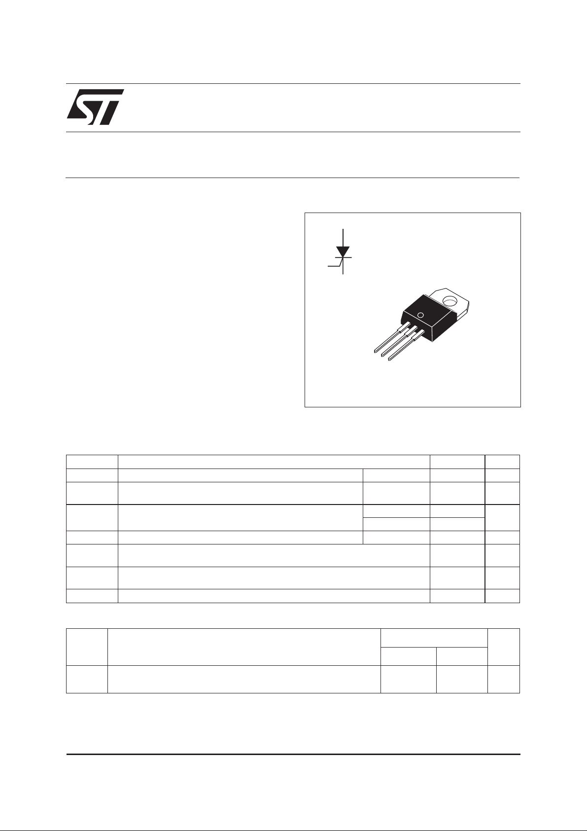
TYN1006
SCR
A
G
K
K
A
G
TO-220AB
ABSOLUTE RATINGS (limiting values)
Symbol Parameter Value Unit
I
T(RMS)
I
T(AV)
I
TSM
2
I
dI/dt Critical rate of rise of on-state current
Tstg
Tj
Tl Maximum lead soldering temperature during 10s at 4.5mm from case 260 °C
Symbol Parameter
V
DRM
V
RRM
RMS on-state current (180° conduction angle) Tc = 110°C 6 A
Average on-state current
(180° conduction angle, single phase circuit)
Non repetitive surge peak on-state current
(Tj initial = 25°C)
tI
2
t value tp = 10ms 24.5 A2s
Gate supply: I
Storage and operating junction temperature range -40 to +150
Repetitive peak off-state voltage
Tj = 125°C
= 100mA dIG/dt = 1A/µs
G
Tc = 110°C 3.8 A
tp = 8.3ms 73 A
tp = 10ms 70
-40 to +125
TYN
606 1006
600 1000 V
50 A/µs
°C
Unit
September 2001 - Ed: 1A
1/4
Page 2
TYN606 TYN1006
THERMAL RESISTANCE
Symbol Parameter Value Unit
Rth (j-a) Junction to ambient 60 °C/W
Rth (j-c) DC Junction to case for DC 2.5 °C/W
GATE CHARACTERISTICS (maximum values)
P
ELECTRICAL CHARACTERISTICS
=1W PGM= 10W (tp = 20µs) I
G(AV)
= 4A (tp = 20µs) V
FGM
RGM
=5V
Symbol Test conditions Value Unit
I
GT
V
GT
V
GD
tgt VD=V
I
I
V
TM
I
DRM
I
RRM
VD= 12V (DC) RL=33Ω Tj = 25°C MAX. 15 mA
VD= 12V (DC) RL=33Ω Tj = 25°C MAX. 1.5 V
VD=V
DRM
DRMIG
dI
/dt = 0.5A/µs
G
IG= 1.2I
L
IT= 100mA Gate open Tj = 25°C MAX. 30 mA
H
GT
RL= 3.3kΩ Tj =110°C MIN. 0.2 V
= 40mA
ITM= 12A tp = 380µs Tj = 25°C MAX. 1.6 V
V
rated
DRM
V
rated
RRM
dV/dt Linear slope up to
tq V
VD= 67% V
=67%V
D
dI
/dt=30 A/µsdVD/dt= 50V/µs
TM
gate open
DRM
DRMITM
= 12A VR= 25V
Fig. 1: Maximum average power dissipation versus average on-state current.
P(W)
7
6
5
4
3
2
1
0
0.0 0.5 1.0 1.5 2.0 2.5 3.0 3.5 4.0 4.5 5.0
360
O
DC
o
=180
o
=120
o
=90
o
=60
o
=30
I(A)
T(AV)
Tj = 25°C TYP. 2 µs
Tj = 25°C TYP. 50 mA
Tj = 25°C MAX. 0.01 mA
Tj = 110°C MAX. 2
Tj = 110°C MIN. 200 V/µs
Tj = 110°C TYP. 70 µs
Fig. 2: Correlation between maximum average
power dissipation and maximum allowable temperatures (Tamb and Tcase) for different thermal
resistances heatsink + contact.
P (W) Tcase ( C)
7
6
5
4
3
2
1
0
0 20 40 60 80 100 120 140
=180
o
Tamb ( C)
o
o
Rth = 0 C/W
o
5C/W
o
10 C/W
o
15 C/W
o
-110
-115
-120
-125
2/4
Page 3

TYN606 TYN1006
Fig. 3: Average on-state current versus case tem-
perature.
I(A)
T(AV)
7
6
5
4
3
2
1
0
0 102030405060708090100110120130
=180
o
Tcase ( C)
DC
o
Fig. 5: Relative variation of gate trigger current
versus junction temperature.
Fig. 4: Relative variation of thermal impedance
versus pulse duration.
Zth/Rth
1
Zth(j-c)
0.1
0.01
1E-3 1E-2 1E-1 1E+0 1E+1 1E+2 5E+2
Zth(j-a)
tp(s)
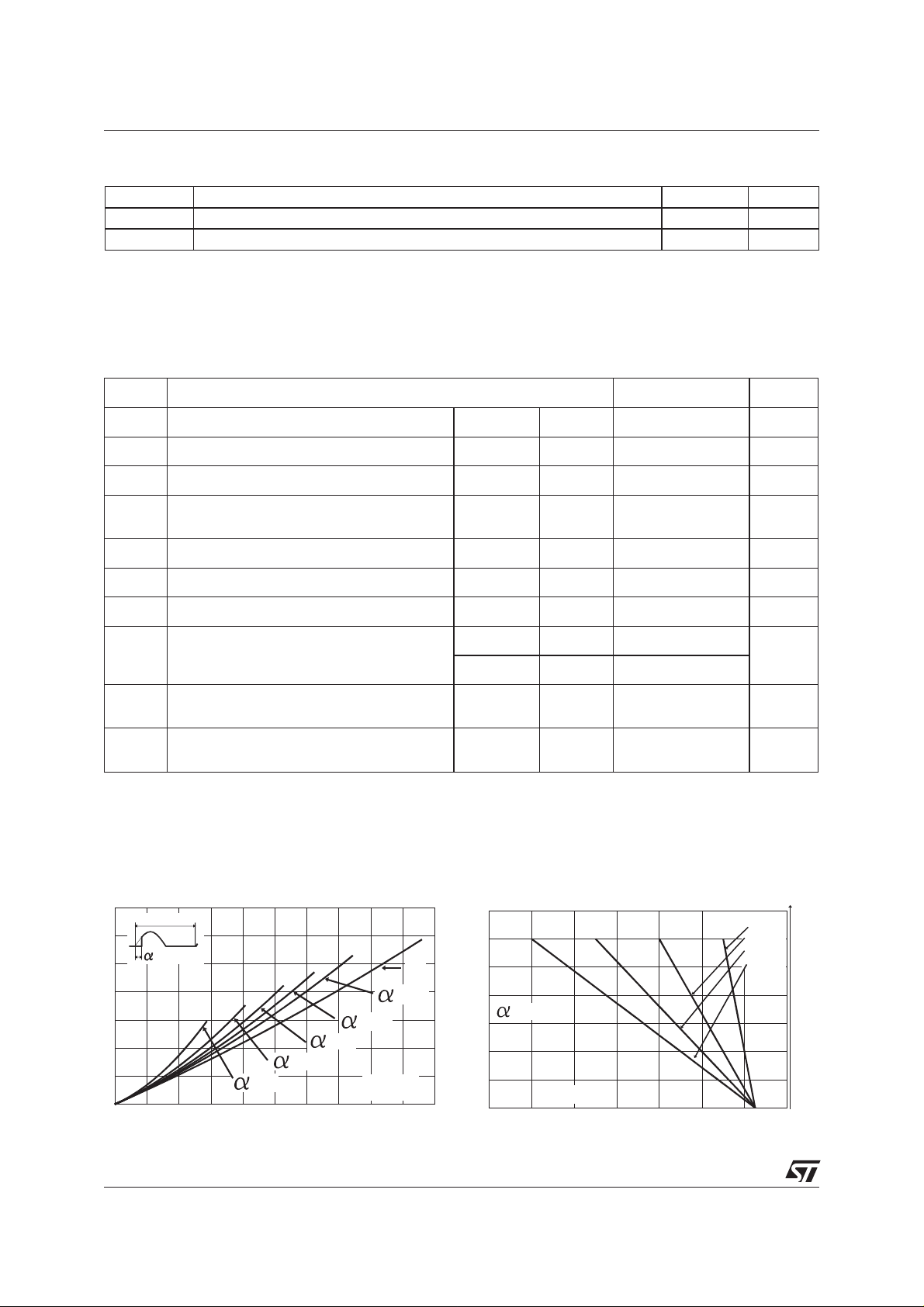
Fig. 6: Non repetitive surge peak on-state current
versus number of cycles.
Fig. 7: Non repetitive surge peak on-state current
forasinusoidalpulsewithwidth: t ≤ 10ms, andcorresponding value of I
2
t.
Fig. 8: On-state characteristics (maximum values).
3/4
Page 4

TYN606 TYN1006
PACKAGE MECHANICAL DATA
TO-220AB (Plastic)
B
L
I
A
l4
a1
l3
l2
a2
b1
e
DIMENSIONS
REF.
C
b2
A 15.20 15.90 0.598 0.625
Millimeters Inches
Min. Typ. Max. Min. Typ. Max.
a1 3.75 0.147
a2 13.00 14.00 0.511 0.551
F
B 10.00 10.40 0.393 0.409
b1 0.61 0.88 0.024 0.034
b2 1.23 1.32 0.048 0.051
C 4.40 4.60 0.173 0.181
c1 0.49 0.70 0.019 0.027
c2
c2 2.40 2.72 0.094 0.107
e 2.40 2.70 0.094 0.106
F 6.20 6.60 0.244 0.259
I 3.75 3.85 0.147 0.151
I4 15.80 16.40 16.80 0.622 0.646 0.661
L 2.65 2.95 0.104 0.116
M
c1
l2 1.14 1.70 0.044 0.066
l3 1.14 1.70 0.044 0.066
M 2.60 0.102
OTHER INFORMATION
Ordering type Marking Package Weight Base qty Delivery mode
TYNxx06 TYNxx06 TO-220AB 2.3 g 250 Bulk
■
Epoxy meets UL94,V0
■
Cooling method: C
■
Recommended torque value: 0.8 m.N.
■
Maximum torque value: 1 m.N.
Informationfurnished isbelieved tobe accurateand reliable.However,STMicroelectronics assumesno responsibilityfor theconsequences of
useof suchinformation norfor anyinfringement ofpatents orother rightsof thirdpartieswhich mayresult fromits use.No licenseis grantedby
implication or otherwise under any patent or patent rights of STMicroelectronics. Specifications mentioned in this publication are subject to
change withoutnotice. This publication supersedesand replaces all informationpreviously supplied.
STMicroelectronics products are not authorized for use as critical componentsin life support devices or systemswithout express written approval ofSTMicroelectronics.
The ST logo is a registered trademark of STMicroelectronics
© 2001 STMicroelectronics - Printed in Italy - All rights reserved.
STMicroelectronics GROUP OF COMPANIES
Australia - Brazil - China - Finland - France - Germany - Hong Kong - India - Italy - Japan - Malaysia
Malta - Morocco - Singapore - Spain - Sweden - Switzerland - United Kingdom - U.S.A.
http://www.st.com
4/4
 Loading...