

Page 1
TVP5020
NTSC/P AL VIDEO DECODER
Data Manual
May 2000 Mixed-Signal Products
SLAS186B
Page 2

IMPORTANT NOTICE
T exas Instruments and its subsidiaries (TI) reserve the right to make changes to their products or to discontinue
any product or service without notice, and advise customers to obtain the latest version of relevant information
to verify, before placing orders, that information being relied on is current and complete. All products are sold
subject to the terms and conditions of sale supplied at the time of order acknowledgement, including those
pertaining to warranty, patent infringement, and limitation of liability.
TI warrants performance of its semiconductor products to the specifications applicable at the time of sale in
accordance with TI’s standard warranty. Testing and other quality control techniques are utilized to the extent
TI deems necessary to support this warranty. Specific testing of all parameters of each device is not necessarily
performed, except those mandated by government requirements.
CERT AIN APPLICATIONS USING SEMICONDUCTOR PRODUCTS MAY INVOLVE POTENTIAL RISKS OF
DEATH, PERSONAL INJURY, OR SEVERE PROPERTY OR ENVIRONMENTAL DAMAGE (“CRITICAL
APPLICATIONS”). TI SEMICONDUCTOR PRODUCTS ARE NOT DESIGNED, AUTHORIZED, OR
WARRANTED TO BE SUITABLE FOR USE IN LIFE-SUPPORT DEVICES OR SYSTEMS OR OTHER
CRITICAL APPLICATIONS. INCLUSION OF TI PRODUCTS IN SUCH APPLICA TIONS IS UNDERSTOOD T O
BE FULLY AT THE CUSTOMER’S RISK.
In order to minimize risks associated with the customer’s applications, adequate design and operating
safeguards must be provided by the customer to minimize inherent or procedural hazards.
TI assumes no liability for applications assistance or customer product design. TI does not warrant or represent
that any license, either express or implied, is granted under any patent right, copyright, mask work right, or other
intellectual property right of TI covering or relating to any combination, machine, or process in which such
semiconductor products or services might be or are used. TI’s publication of information regarding any third
party’s products or services does not constitute TI’s approval, warranty or endorsement thereof.
Copyright 2000, Texas Instruments Incorporated
Page 3

iii
Contents
Section Title Page
1 Introduction 1–1. . . . . . . . . . . . . . . . . . . . . . . . . . . . . . . . . . . . . . . . . . . . . . . . . . . . . . . . . . . . . . .
1.1 Features 1–1. . . . . . . . . . . . . . . . . . . . . . . . . . . . . . . . . . . . . . . . . . . . . . . . . . . . . . . . . . . . . .
1.2 Applications 1–2. . . . . . . . . . . . . . . . . . . . . . . . . . . . . . . . . . . . . . . . . . . . . . . . . . . . . . . . . . .
1.3 Functional Block Diagram 1–2. . . . . . . . . . . . . . . . . . . . . . . . . . . . . . . . . . . . . . . . . . . . . . .
1.4 Terminal Assignments 1–3. . . . . . . . . . . . . . . . . . . . . . . . . . . . . . . . . . . . . . . . . . . . . . . . . .
1.5 Ordering Information 1–3. . . . . . . . . . . . . . . . . . . . . . . . . . . . . . . . . . . . . . . . . . . . . . . . . . .
1.6 Terminal Functions 1–4. . . . . . . . . . . . . . . . . . . . . . . . . . . . . . . . . . . . . . . . . . . . . . . . . . . . .
2 Detailed Description 2–1. . . . . . . . . . . . . . . . . . . . . . . . . . . . . . . . . . . . . . . . . . . . . . . . . . . . . . .
2.1 Analog Video Processors and A/D Converter 2–1. . . . . . . . . . . . . . . . . . . . . . . . . . . . . .
2.1.1 Video Input Selection 2–1. . . . . . . . . . . . . . . . . . . . . . . . . . . . . . . . . . . . . . . . . . . . .
2.1.2 Analog Input Clamping and Automatic Gain Control Circuits 2–1. . . . . . . . . . .
2.1.3 A/D Converter 2–1. . . . . . . . . . . . . . . . . . . . . . . . . . . . . . . . . . . . . . . . . . . . . . . . . . .
2.2 Digital Processing 2–1. . . . . . . . . . . . . . . . . . . . . . . . . . . . . . . . . . . . . . . . . . . . . . . . . . . . . .
2.2.1 Y/C Separation 2–2. . . . . . . . . . . . . . . . . . . . . . . . . . . . . . . . . . . . . . . . . . . . . . . . . .
2.2.2 Luminance Processing 2–3. . . . . . . . . . . . . . . . . . . . . . . . . . . . . . . . . . . . . . . . . . .
2.2.3 Chrominance Processing 2–6. . . . . . . . . . . . . . . . . . . . . . . . . . . . . . . . . . . . . . . . .
2.2.4 Clock Circuits 2–6. . . . . . . . . . . . . . . . . . . . . . . . . . . . . . . . . . . . . . . . . . . . . . . . . . .
2.3 Video Output Format 2–7. . . . . . . . . . . . . . . . . . . . . . . . . . . . . . . . . . . . . . . . . . . . . . . . . . .
2.3.1 Sampling Frequencies and Patterns 2–7. . . . . . . . . . . . . . . . . . . . . . . . . . . . . . . .
2.3.2 Video Port 16-Bit 4:2:2 Output Format Timing 2–8. . . . . . . . . . . . . . . . . . . . . . . .
2.3.3 Video Port 12-Bit 4:1:1 Output Format Timing 2–9. . . . . . . . . . . . . . . . . . . . . . . .
2.3.4 Video Port 8-Bit 4:2:2 and ITU-R BT.656 Output Format Timing 2–9. . . . . . . .
2.4 Synchronization Signals 2–9. . . . . . . . . . . . . . . . . . . . . . . . . . . . . . . . . . . . . . . . . . . . . . . .
2.5 I
2
C/VIP/VMI Host Interface 2–12. . . . . . . . . . . . . . . . . . . . . . . . . . . . . . . . . . . . . . . . . . . . .
2.6 I2C Interface 2–12. . . . . . . . . . . . . . . . . . . . . . . . . . . . . . . . . . . . . . . . . . . . . . . . . . . . . . . . .
2.6.1 I2C Host Port Select 2–13. . . . . . . . . . . . . . . . . . . . . . . . . . . . . . . . . . . . . . . . . . . . .
2.6.2 I2C Write Operation 2–14. . . . . . . . . . . . . . . . . . . . . . . . . . . . . . . . . . . . . . . . . . . . .
2.6.3 I2C Read Operation 2–15. . . . . . . . . . . . . . . . . . . . . . . . . . . . . . . . . . . . . . . . . . . . .
2.6.4 I
2
C Microcode Write Operation 2–16. . . . . . . . . . . . . . . . . . . . . . . . . . . . . . . . . . .
2.6.5 I2C Microcode Read Operation 2–17. . . . . . . . . . . . . . . . . . . . . . . . . . . . . . . . . . .
2.7 VIP Host Interface Port 2–19. . . . . . . . . . . . . . . . . . . . . . . . . . . . . . . . . . . . . . . . . . . . . . . .
2.7.1 VIP Host Port Terminal Description 2–20. . . . . . . . . . . . . . . . . . . . . . . . . . . . . . . .
2.7.2 VIP Phases 2–20. . . . . . . . . . . . . . . . . . . . . . . . . . . . . . . . . . . . . . . . . . . . . . . . . . . .
2.7.3 Command Byte 2–21. . . . . . . . . . . . . . . . . . . . . . . . . . . . . . . . . . . . . . . . . . . . . . . . .
2.7.4 VIP Microcode Write Operation 2–26. . . . . . . . . . . . . . . . . . . . . . . . . . . . . . . . . . .
2.7.5 VIP Microcode Read Operation 2–26. . . . . . . . . . . . . . . . . . . . . . . . . . . . . . . . . . .
2.8 Video Module Interface (VMI) Host Interface 2–26. . . . . . . . . . . . . . . . . . . . . . . . . . . . . .
2.9 Host Port – Mode A Timing 2–27. . . . . . . . . . . . . . . . . . . . . . . . . . . . . . . . . . . . . . . . . . . . .
2.10 Host Port – Mode B Timing 2–28. . . . . . . . . . . . . . . . . . . . . . . . . . . . . . . . . . . . . . . . . . . . .
2.11 Host Port – Mode C Timing (PPC) 2–28. . . . . . . . . . . . . . . . . . . . . . . . . . . . . . . . . . . . . . .
Page 4

iv
2.11.1 VMI Register Mapping 2–29. . . . . . . . . . . . . . . . . . . . . . . . . . . . . . . . . . . . . . . . . .
2.11.2 VMI Microcode Write Operation 2–30. . . . . . . . . . . . . . . . . . . . . . . . . . . . . . . . . .
2.11.3 VMI Microcode Read Operation 2–31. . . . . . . . . . . . . . . . . . . . . . . . . . . . . . . . . .
2.12 Genlock Control 2–31. . . . . . . . . . . . . . . . . . . . . . . . . . . . . . . . . . . . . . . . . . . . . . . . . . . . . .
2.13 VBI Data Processor 2–32. . . . . . . . . . . . . . . . . . . . . . . . . . . . . . . . . . . . . . . . . . . . . . . . . . .
2.13.1 Teletext Data Byte Order 2–32. . . . . . . . . . . . . . . . . . . . . . . . . . . . . . . . . . . . . . . . .
2.13.2 Teletext as Ancillary Data in Video Stream 2–33. . . . . . . . . . . . . . . . . . . . . . . . .
2.14 Reset 2–36. . . . . . . . . . . . . . . . . . . . . . . . . . . . . . . . . . . . . . . . . . . . . . . . . . . . . . . . . . . . . . .
2.15 Internal Control Registers 2–37. . . . . . . . . . . . . . . . . . . . . . . . . . . . . . . . . . . . . . . . . . . . . .
2.15.1 Register Definitions 2–38. . . . . . . . . . . . . . . . . . . . . . . . . . . . . . . . . . . . . . . . . . . . .
2.15.2 Vendor ID 2–38. . . . . . . . . . . . . . . . . . . . . . . . . . . . . . . . . . . . . . . . . . . . . . . . . . . . .
2.15.3 Device ID 2–39. . . . . . . . . . . . . . . . . . . . . . . . . . . . . . . . . . . . . . . . . . . . . . . . . . . . .
2.15.4 Subsystem Vendor ID 2–39. . . . . . . . . . . . . . . . . . . . . . . . . . . . . . . . . . . . . . . . . . .
2.15.5 Subsystem Device ID 2–39. . . . . . . . . . . . . . . . . . . . . . . . . . . . . . . . . . . . . . . . . . .
2.15.6 Subsystem Revision ID 2–39. . . . . . . . . . . . . . . . . . . . . . . . . . . . . . . . . . . . . . . . .
2.15.7 Analog Input Source Selection 2–40. . . . . . . . . . . . . . . . . . . . . . . . . . . . . . . . . . .
2.15.8 Analog Channel Controls 2–41. . . . . . . . . . . . . . . . . . . . . . . . . . . . . . . . . . . . . . . .
2.15.9 Operation Mode Controls 2–42. . . . . . . . . . . . . . . . . . . . . . . . . . . . . . . . . . . . . . . .
2.15.10 Miscellaneous Controls 2–43. . . . . . . . . . . . . . . . . . . . . . . . . . . . . . . . . . . . . . . . .
2.15.11 Color Killer Threshold Control 2–44. . . . . . . . . . . . . . . . . . . . . . . . . . . . . . . . . . .
2.15.12 Luminance Processing Control 1 2–45. . . . . . . . . . . . . . . . . . . . . . . . . . . . . . . .
2.15.13 Luminance Processing Control 2 2–46. . . . . . . . . . . . . . . . . . . . . . . . . . . . . . . .
2.15.14 Brightness Control 2–47. . . . . . . . . . . . . . . . . . . . . . . . . . . . . . . . . . . . . . . . . . . . .
2.15.15 Color Saturation Control 2–47. . . . . . . . . . . . . . . . . . . . . . . . . . . . . . . . . . . . . . . .
2.15.16 Hue Control 2–47. . . . . . . . . . . . . . . . . . . . . . . . . . . . . . . . . . . . . . . . . . . . . . . . . . .
2.15.17 Contrast Control 2–48. . . . . . . . . . . . . . . . . . . . . . . . . . . . . . . . . . . . . . . . . . . . . . .
2.15.18 Outputs and Data Rates Select 2–48. . . . . . . . . . . . . . . . . . . . . . . . . . . . . . . . . .
2.15.19 Horizontal Sync (HSYN) Start 2–49. . . . . . . . . . . . . . . . . . . . . . . . . . . . . . . . . . .
2.15.20 Vertical Blanking Start 2–49. . . . . . . . . . . . . . . . . . . . . . . . . . . . . . . . . . . . . . . . . .
2.15.21 Vertical Blanking Stop 2–50. . . . . . . . . . . . . . . . . . . . . . . . . . . . . . . . . . . . . . . . . .
2.15.22 Chrominance Control 2–51. . . . . . . . . . . . . . . . . . . . . . . . . . . . . . . . . . . . . . . . . .
2.15.23 Digital Channel Selection 2–52. . . . . . . . . . . . . . . . . . . . . . . . . . . . . . . . . . . . . . .
2.15.24 Firmware Version 2–52. . . . . . . . . . . . . . . . . . . . . . . . . . . . . . . . . . . . . . . . . . . . . .
2.15.25 Status Register 1 2–53. . . . . . . . . . . . . . . . . . . . . . . . . . . . . . . . . . . . . . . . . . . . . .
2.15.26 Status Register 2 2–54. . . . . . . . . . . . . . . . . . . . . . . . . . . . . . . . . . . . . . . . . . . . . .
2.15.27 AGC Gain 2–54. . . . . . . . . . . . . . . . . . . . . . . . . . . . . . . . . . . . . . . . . . . . . . . . . . . .
2.15.28 TXF Filter #1 Parameters 2–55. . . . . . . . . . . . . . . . . . . . . . . . . . . . . . . . . . . . . . .
2.15.29 TXF Filter #2 Parameters 2–56. . . . . . . . . . . . . . . . . . . . . . . . . . . . . . . . . . . . . . .
2.15.30 TXF Error Filtering Enables 2–57. . . . . . . . . . . . . . . . . . . . . . . . . . . . . . . . . . . . .
2.15.31 TXF Transaction Processing Enables 2–57. . . . . . . . . . . . . . . . . . . . . . . . . . . .
2.15.32 TTX Control Register 2–58. . . . . . . . . . . . . . . . . . . . . . . . . . . . . . . . . . . . . . . . . . .
2.15.33 Line Enable Registers 2–58. . . . . . . . . . . . . . . . . . . . . . . . . . . . . . . . . . . . . . . . . .
2.15.34 Sync Pattern Register 2–59. . . . . . . . . . . . . . . . . . . . . . . . . . . . . . . . . . . . . . . . . .
2.15.35 Teletext FIFO 2–59. . . . . . . . . . . . . . . . . . . . . . . . . . . . . . . . . . . . . . . . . . . . . . . . .
2.15.36 Closed Caption Data 2–59. . . . . . . . . . . . . . . . . . . . . . . . . . . . . . . . . . . . . . . . . .
2.15.37 Buffer Status 2–60. . . . . . . . . . . . . . . . . . . . . . . . . . . . . . . . . . . . . . . . . . . . . . . . .
2.15.38 Interrupt Threshold 2–60. . . . . . . . . . . . . . . . . . . . . . . . . . . . . . . . . . . . . . . . . . . .
Page 5

v
2.15.39 Interrupt Line Number 2–60. . . . . . . . . . . . . . . . . . . . . . . . . . . . . . . . . . . . . . . . . .
2.15.40 FIFO Control 2–61. . . . . . . . . . . . . . . . . . . . . . . . . . . . . . . . . . . . . . . . . . . . . . . . . .
2.15.41 Interrupt Status Register 2–62. . . . . . . . . . . . . . . . . . . . . . . . . . . . . . . . . . . . . . . .
2.15.42 Interrupt Enable Register 2–63. . . . . . . . . . . . . . . . . . . . . . . . . . . . . . . . . . . . . . .
2.15.43 Interrupt Configuration Register 2–63. . . . . . . . . . . . . . . . . . . . . . . . . . . . . . . . .
2.15.44 Interrupt Status Register 2–63. . . . . . . . . . . . . . . . . . . . . . . . . . . . . . . . . . . . . . . .
3 Electrical Specifications 3–1. . . . . . . . . . . . . . . . . . . . . . . . . . . . . . . . . . . . . . . . . . . . . . . . . . .
3.1 Absolute Maximum Ratings† 3–1. . . . . . . . . . . . . . . . . . . . . . . . . . . . . . . . . . . . . . . . . . . .
3.2 Recommended Operating Conditions 3–1. . . . . . . . . . . . . . . . . . . . . . . . . . . . . . . . . . . . .
3.3 Electrical Characteristics 3–2. . . . . . . . . . . . . . . . . . . . . . . . . . . . . . . . . . . . . . . . . . . . . . . .
3.3.1 Analog Processing and Analog-to-Digital Converter 3–2. . . . . . . . . . . . . . . . . .
3.3.2 DC Electrical Characteristics 3–2. . . . . . . . . . . . . . . . . . . . . . . . . . . . . . . . . . . . . .
3.4 Timing 3–3. . . . . . . . . . . . . . . . . . . . . . . . . . . . . . . . . . . . . . . . . . . . . . . . . . . . . . . . . . . . . . . .
3.4.1 Clocks, Video Data, Sync Timing 3–3. . . . . . . . . . . . . . . . . . . . . . . . . . . . . . . . . . .
3.4.2 I
2
C Host Bus Timing 3–4. . . . . . . . . . . . . . . . . . . . . . . . . . . . . . . . . . . . . . . . . . . . .
3.4.3 VIP Host Port Timing 3–4. . . . . . . . . . . . . . . . . . . . . . . . . . . . . . . . . . . . . . . . . . . . .
3.4.4 VMI Host Port Timing (Mode A) 3–5. . . . . . . . . . . . . . . . . . . . . . . . . . . . . . . . . . . .
3.4.5 VMI Host Port Timing (Mode B) 3–6. . . . . . . . . . . . . . . . . . . . . . . . . . . . . . . . . . . .
4 Mechanical Data 4–1. . . . . . . . . . . . . . . . . . . . . . . . . . . . . . . . . . . . . . . . . . . . . . . . . . . . . . . . . . .
Page 6

vi
List of Illustrations
Figure Title Page
2–1 Analog Video Processors and A/D Converter 2–1. . . . . . . . . . . . . . . . . . . . . . . . . . . . . . . . . .
2–2 Digital Video Signal Processing Block Diagram 2–2. . . . . . . . . . . . . . . . . . . . . . . . . . . . . . . .
2–3 Chroma Trap Filter Frequency Response for 13.5 MHz Sampling 2–3. . . . . . . . . . . . . . . .
2–4 Chroma Trap Filter Frequency Response for Square-Pixel Sampling 2–3. . . . . . . . . . . . .
2–5 Luminance Edge-Enhancer 2–4. . . . . . . . . . . . . . . . . . . . . . . . . . . . . . . . . . . . . . . . . . . . . . . . .
2–6 Peaking Filter Response, 13.5 MHz Sampling 2–4. . . . . . . . . . . . . . . . . . . . . . . . . . . . . . . . .
2–7 Peaking Filter Response, NTSC AND PAL-M SQUARE PIXEL 2–5. . . . . . . . . . . . . . . . . . .
2–8 Peaking Filter Response, PAL Square Pixel 2–5. . . . . . . . . . . . . . . . . . . . . . . . . . . . . . . . . . .
2–9 Transfer Curve of Coring Circuit 2–6. . . . . . . . . . . . . . . . . . . . . . . . . . . . . . . . . . . . . . . . . . . . .
2–10 Clock Circuit Diagram 2–6. . . . . . . . . . . . . . . . . . . . . . . . . . . . . . . . . . . . . . . . . . . . . . . . . . . . .
2–11 Reference Clock Configurations 2–7. . . . . . . . . . . . . . . . . . . . . . . . . . . . . . . . . . . . . . . . . . . .
2–12 4:2:2 Sampling 2–8. . . . . . . . . . . . . . . . . . . . . . . . . . . . . . . . . . . . . . . . . . . . . . . . . . . . . . . . . . .
2–13 4:1:1 Sampling 2–8. . . . . . . . . . . . . . . . . . . . . . . . . . . . . . . . . . . . . . . . . . . . . . . . . . . . . . . . . . .
2–14 16-Bit 4:2:2 Output Format 2–8. . . . . . . . . . . . . . . . . . . . . . . . . . . . . . . . . . . . . . . . . . . . . . . . .
2–15 12-bit 4:1:1 Output Format 2–9. . . . . . . . . . . . . . . . . . . . . . . . . . . . . . . . . . . . . . . . . . . . . . . . .
2–16 8-Bit 4:2:2 and ITU-R BT.656 Output Formats 2–9. . . . . . . . . . . . . . . . . . . . . . . . . . . . . . . .
2–17 Vertical Synchronization Signals 2–10. . . . . . . . . . . . . . . . . . . . . . . . . . . . . . . . . . . . . . . . . . .
2–18 Horizontal Synchronization Signals 2–1 1. . . . . . . . . . . . . . . . . . . . . . . . . . . . . . . . . . . . . . . . .
2–19 Host Interface 2–12. . . . . . . . . . . . . . . . . . . . . . . . . . . . . . . . . . . . . . . . . . . . . . . . . . . . . . . . . . .
2–20 I
2
C Data Transfer Example 2–13. . . . . . . . . . . . . . . . . . . . . . . . . . . . . . . . . . . . . . . . . . . . . . .
2–21 VIP Transfer Example 2–20. . . . . . . . . . . . . . . . . . . . . . . . . . . . . . . . . . . . . . . . . . . . . . . . . . . .
2–22 Functional Timing Reading From TVP (Example) 2–22. . . . . . . . . . . . . . . . . . . . . . . . . . . .
2–23 Functional Timing Writing to TVP (Example) 2–23. . . . . . . . . . . . . . . . . . . . . . . . . . . . . . . . .
2–24 Functional Timing Reading From FIFO (Example) 2–23. . . . . . . . . . . . . . . . . . . . . . . . . . . .
2–25 Functional Timing Example of Slave Termination 2–24. . . . . . . . . . . . . . . . . . . . . . . . . . . . .
2–26 VMI Host Port Mode A Timing 2–27. . . . . . . . . . . . . . . . . . . . . . . . . . . . . . . . . . . . . . . . . . . . .
2–27 Host Port Mode B Timing 2–28. . . . . . . . . . . . . . . . . . . . . . . . . . . . . . . . . . . . . . . . . . . . . . . . .
2–28 Host Port Mode C Timing 2–28. . . . . . . . . . . . . . . . . . . . . . . . . . . . . . . . . . . . . . . . . . . . . . . . .
2–29 VMI Address Register Map 2–29. . . . . . . . . . . . . . . . . . . . . . . . . . . . . . . . . . . . . . . . . . . . . . . .
2–30 GLCO Timing 2–32. . . . . . . . . . . . . . . . . . . . . . . . . . . . . . . . . . . . . . . . . . . . . . . . . . . . . . . . . . .
2–31 Video Input Source Selection 2–40. . . . . . . . . . . . . . . . . . . . . . . . . . . . . . . . . . . . . . . . . . . . . .
3–1 Clock, Video and Sync Timing 3–3. . . . . . . . . . . . . . . . . . . . . . . . . . . . . . . . . . . . . . . . . . . . . . .
3–2 I
2
C Bus Timing 3–4. . . . . . . . . . . . . . . . . . . . . . . . . . . . . . . . . . . . . . . . . . . . . . . . . . . . . . . . . . . .
3–3 VIP Host Port Timing 3–4. . . . . . . . . . . . . . . . . . . . . . . . . . . . . . . . . . . . . . . . . . . . . . . . . . . . . . .
3–4 VMI Host Port Timing (Mode A) 3–5. . . . . . . . . . . . . . . . . . . . . . . . . . . . . . . . . . . . . . . . . . . . . .
3–5 VMI Host Port Timing (Mode B) 3–6. . . . . . . . . . . . . . . . . . . . . . . . . . . . . . . . . . . . . . . . . . . . . .
Page 7

vii
List of Tables
Table Title Page
2–1 Summary of the Line Frequencies, Data Rates, and Pixel Counts 2–7. . . . . . . . . . . . . . . .
2–2 Host Port Select 2–12. . . . . . . . . . . . . . . . . . . . . . . . . . . . . . . . . . . . . . . . . . . . . . . . . . . . . . . . . .
2–3 I2C Host Port Terminal Description 2–13. . . . . . . . . . . . . . . . . . . . . . . . . . . . . . . . . . . . . . . . . .
2–4 VIP Host Port Terminal Description 2–20. . . . . . . . . . . . . . . . . . . . . . . . . . . . . . . . . . . . . . . . . .
2–5 VIP Host Port Phase Description 2–21. . . . . . . . . . . . . . . . . . . . . . . . . . . . . . . . . . . . . . . . . . . .
2–6 Condensed Table Command/Address 2–21. . . . . . . . . . . . . . . . . . . . . . . . . . . . . . . . . . . . . . .
2–7 VMI Host Port Select 2–26. . . . . . . . . . . . . . . . . . . . . . . . . . . . . . . . . . . . . . . . . . . . . . . . . . . . . .
2–8 VMI Host Port Terminal Definitions 2–27. . . . . . . . . . . . . . . . . . . . . . . . . . . . . . . . . . . . . . . . . .
2–9 Teletext Byte Order 2–32. . . . . . . . . . . . . . . . . . . . . . . . . . . . . . . . . . . . . . . . . . . . . . . . . . . . . . . .
2–10 NABTS 525/625-Line Ancillary Data Sequence 2–34. . . . . . . . . . . . . . . . . . . . . . . . . . . . . .
2–11 WST 525-Line Ancillary Data Sequence 2–35. . . . . . . . . . . . . . . . . . . . . . . . . . . . . . . . . . . .
2–12 WST 625-Line Ancillary Data Sequence 2–35. . . . . . . . . . . . . . . . . . . . . . . . . . . . . . . . . . . .
2–13 Dummy Timing Ancillary Data Sequence 2–36. . . . . . . . . . . . . . . . . . . . . . . . . . . . . . . . . . . .
2–14 Ancillary Data ID 2–36. . . . . . . . . . . . . . . . . . . . . . . . . . . . . . . . . . . . . . . . . . . . . . . . . . . . . . . . .
2–15 Power-Up Reset Sequence 2–36. . . . . . . . . . . . . . . . . . . . . . . . . . . . . . . . . . . . . . . . . . . . . . .
2–16 Registers Summary 2–37. . . . . . . . . . . . . . . . . . . . . . . . . . . . . . . . . . . . . . . . . . . . . . . . . . . . . .
2–17 Analog Channel and Video Mode Selection 2–40. . . . . . . . . . . . . . . . . . . . . . . . . . . . . . . . .
2–18 YUV Output Controls 2–43. . . . . . . . . . . . . . . . . . . . . . . . . . . . . . . . . . . . . . . . . . . . . . . . . . . . .
Page 8

viii
Page 9

1–1
1 Introduction
The TVP5020 is a high-quality single-chip digital video decoder that converts base-band analog NTSC and
PAL video signals into digital component video. Sampling is square-pixel or ITU-R BT.601 (13.5 MHz) and
is line-locked for correct pixel alignment. The output formats can be 8-bit or 16-bit 4:2:2, 12-bit 4:1:1, or 8-bit
ITU-R BT.656. The TVP5020 uses TI patented technology for locking to weak, noisy, or unstable signals.
A genlock control output is generated for synchronizing downstream video encoders.
Two-line (1-H delay) comb filtering is available for both the luma and chroma data paths to reduce both
cross-luma and cross-chroma artifacts; a chroma trap filter is also available. Video characteristics including
hue, contrast, and saturation are programmable using one of five supported host port interfaces. The
TVP5020 generates synchronization, blanking, field, lock, and clock signals in addition to digital video
outputs.
The TVP5020 includes advanced vertical blanking interval (VBI) data retrieval. The VBI data processor
slices, parses, and performs error checking on teletext data in several formats. A built-in FIFO stores up to
14 lines of teletext data and, with proper host port synchronization, full-field teletext retrieval is possible. The
VBI data processor also retrieves closed-caption data.
The main blocks of TVP5020 include:
• Analog processors and A/D converter
• Y/C separation
• Chrominance processor
• Luminance processor
• Clock/Timing processor and power-down control
• Output formatter
• Host port interface
• VBI data processor
1.1 Features
• NTSC (M) and PAL (B, D, G, H, I, M, N) composite video
• Two analog video inputs for up to two composite inputs
• Single built-in-analog signal processing channels with clamping and AGC
• Single high speed 8-bit A/D converter
• Patented architecture for locking to weak, noisy, or unstable signals
• Comb filters for both cross-color and cross-luminance noise reductions
• Line locked clock and sampling
• Programmable data rates:
– 12.2727 MHz square-pixel (NTSC)
– 14.7500 MHz square-pixel (PAL)
– 13.5 MHz ITU-R BT.601 (NTSC and PAL)
• Programmable output formats: 16-bit or 8-bit 4:2:2 YCbCr, 12-Bit 4:1:1 YCbCr and ITU-R BT.656
with embedded syncs
Page 10
1–2
• Teletext (NABTS, WST) and closed caption decode with FIFO
• ITU-R BT.601 or extended coding range
• Programmable host port options including I
2
C, VMI (3 modes), and VIP
• 80-terminal TQFP package
1.2 Applications
• Digital image processing
• Video conferencing
• Multimedia
• Digital video
• Desktop video
• Video capture
• Video editing
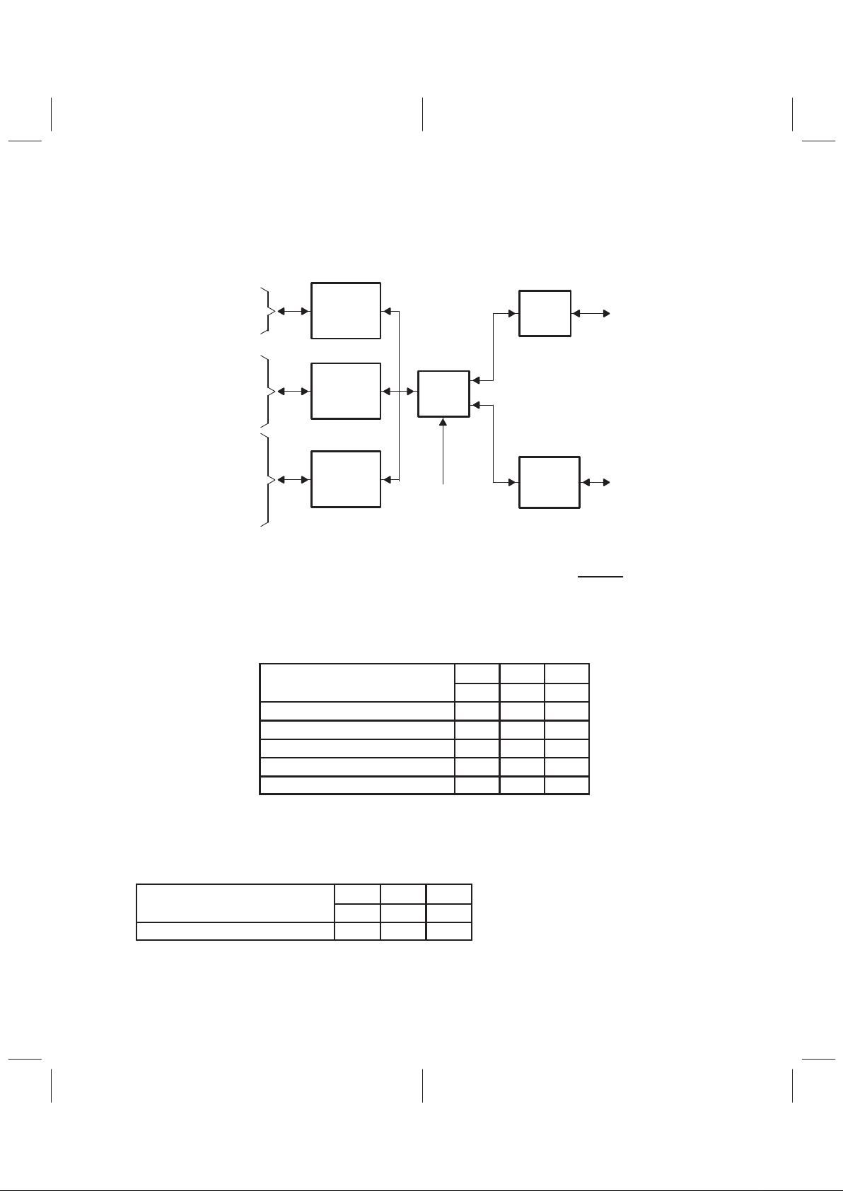
1.3 Functional Block Diagram
A/D
AGC
Luma/Chroma
Separation
Luminance
Processing
Chrominance
Processing
Output
Formatter
Line
and
Chroma
PLL’s
Sync
Processor
VI1A
VI1B
XTAL1
XTAL2
SCLK
PCLK
PREF
GLCO
Y (7:0)
UV (7:0)
OEB
HSYN
VSYN
FID
PALI
GPCL
RSTINB
VMI Interface
VBI
D (7:0)
A0
VC (0–3)
INTREQ
M
U
X
Channel 1
I2C Interface
A1
M
U
X
Page 11

1–3
1.4 Terminal Assignments
TQFP PACKAGE
(TOP VIEW)
22 23
UV7
UV6
UV5
DGND
UV4
UV3
DVDD
UV2
UV1
UV0
Y7
Y6
Y5
DGND
Y4
Y3
DVDD
Y2
Y1
Y0
60
59
58
57
56
55
54
53
52
51
50
49
48
47
46
45
44
43
42
41
24
1
2
3
4
5
6
7
8
9
10
11
12
13
14
15
16
17
18
19
20
NC
NC
CH1_AGND
VI_1B
VI_1A
CH1_AVDD
REFM
REFP
AVDD
NC
NC
AGND
NC
NC
NC
AFE_GND
NSUB
AFE_VDD
DTO_AVDD
DTO_AGND
25 26 27 28
D5
79 78 77 76 7580 74
VC1
VC2
VC3
DVDDA1A0
D7
GLCO
FID
RSTINB
DGND
PLL_AVDD
GPCL
AVID
PLL_BYP
VSYN
72 71 7073
29 30 31 32 33
69 68
21
DGND
DGND
67 66 65 64
34 35 36 37
DVDD
XTAL1
XTAL2
DGND
D3D2DVDD
D1
INTREQ
VC0
SCLK
PREF
38 39 40
D0
OEB
63 62 61
D4
EXT_DATA_8
DGND
PALI
PCLK
HSYN
D6
1.5 Ordering Information
DEVICE: TVP5020CPFP
PFP: Plastic flat-pack with PowerPAD
Page 12
1–4
1.6 Terminal Functions
TERMINAL
NAME NO.
I/O
DESCRIPTIONS
Analog video
VI_1A
VI_1B
5
4
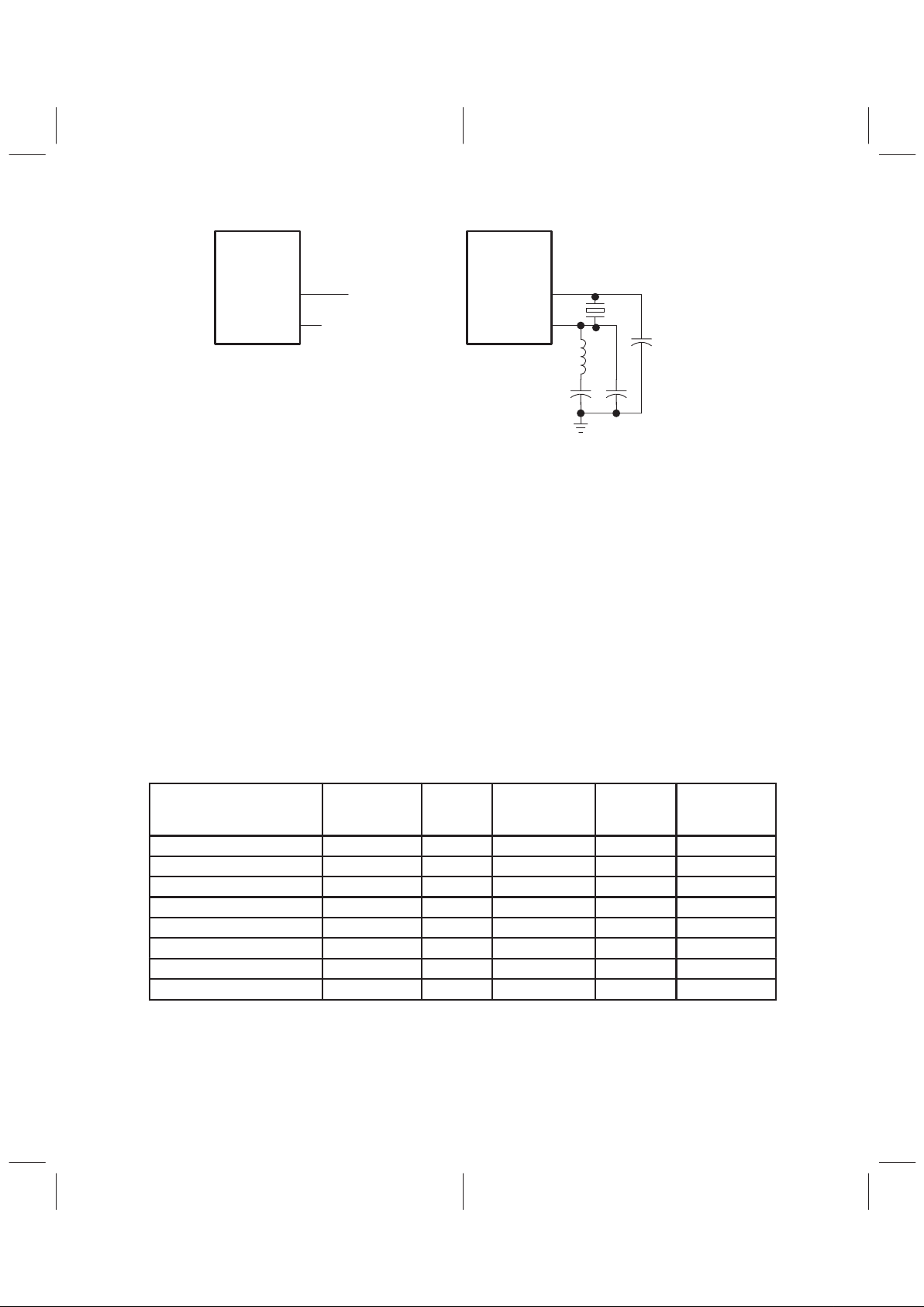
I Analog video inputs. Up to two composite inputs. The inputs must be AC coupled. The
recommended coupling capacitor is 0.1 µF.
Clock Signals
PCLK 40 O Pixel clock output. The frequency is 12.2727 MHz for square-pixel NTSC,
14.75 MHz for square-pixel PAL, and 13.5 MHz for ITU-R BT.601 sampling modes.
PREF 39 O Clock phase reference signal. This signal qualifies clock edges when SCLK is used to
clock data that is changing at the pixel clock rate.
SCLK 38 O System clock output with twice the frequency of the pixel clock (PCLK).
XTAL1
XTAL2
35
36
I External clock reference. The user may connect XTAL1 to a TTL-compatible
oscillator or to one terminal of a crystal oscillator. The user may connect XT AL2 to the
other terminal of the crystal oscillator or not connect XTAL2 at all. Square pixel
sampling uses an oscillator frequency of 26.800 MHz. ITU-R BT.601 sampling uses
an oscillator frequency of 24.576 MHz.
Digital Video
EXT_DATA_8 61 I Bit [8] of a 9-or 10-bit digital composite video input
UV[0:7] 51, 52,
53, 55,
56, 58,
59, 60
I/O Digital chrominance outputs. These terminals may be configured to output data from
the channel 2 A/D converter. A vendor modifiable subsystem ID may be initialized by
configuring the UV [7:0] terminals with pull-up/pull-down resistors.
Y[0:7] 41, 42,
43, 45,
46, 48,
49, 50
O Digital luminance outputs, or multiplexed luminance and chrominance outputs.
These terminals may be configured to output data from the channel 1 A/D converter.
HOST PORT-bus VMI I2C VIP
A[0:1] 73, 74 I VMI address port
D[0:7] 63, 64
66, 67
69, 70
71, 72
I/O VMI data port – bit [7:0].
INTREQ 80 O Interrupt request (INTREQ) Interrupt request (VIRQ)
VC0 79 I/O VMI port data ack. or ready
signal (DTACK)
Serial clock (SCL) Hardware address
bit-0 (HAD[0])
VC1 78 I/O VMI Port Read-Write or
Write (RW/WR)
Serial data (SDA) Hardware address bit-1
HAD[1]
VC2 77 I/O VMI port data strobe or read
signal (DS/RD)
Hardware control (HCTL)
VC3 76 I VMI port chip select. (VC) Slave address select
(I2CA)
VIPCLK
Page 13

1–5
1.6 Terminal Functions (Continued)
TERMINAL
NAME NO.
I/O
DESCRIPTIONS
Miscellaneous signals
GPCL 26 I/O General-purpose control logic. This terminal has three functions:
1. General-purpose output. In this mode the state of GPCL is directly
programmed via the host port.
2. Vertical blank output. In this mode the GPCL terminal is used to indicate
the vertical blanking interval of the output video. The beginning and end
times of this signal are programmable via the host port control.
3. Sync lock control input. In this mode when GPCL is high, the output clock
frequencies and sync timing are forced to nominal values.
GLCO 31 I/O This serial output carries color PLL information. A slave device can decode the
information to allow genlocking to the TVP5020. Data is transmitted at the SCLK
rate. Additionally, this terminal, in conjunction with PALI and FID, is used to
determine the host port mode configuration during initial power up.
OEB 62 I Output enable for Y and UV terminals. Output enable is also controllable via the
host port.
PLL_BYP 28 Connect a 0.1 µF capacitor between this terminal and PLL_AVDD
RSTINB 23 I Reset input, active low
NC 1, 2, 13,
14, 15
Not connected
Power Supplies
AFE_GND 16 Analog ground
AFE_VDD 18 Analog supply, connect to 5 V
CH1_AGND
AGND
3
12
Analog grounds
CH1_AVDD
AVDD
6
9
Analog supply , connect to 5 V
DGND 21, 22, 24,
37, 47, 57,
68
Digital grounds
DTO_AGND 20 DTO ground, connect to analog ground
DTO_A VDD 19 DTO supply , connect to 5 V analog
DVDD 34, 44, 54,
65, 75
Digital supply, connect to 3.3 V
NSUB 17 Substrate ground, connect to analog ground
PLL_AVDD 25 PLL supply connect to 3.3 V
REFP 8 A/D reference supply, connect to 5 V analog
REFM 7 A/D reference ground, connect to analog ground
Page 14

1–6
1.6 Terminal Functions (Continued)
TERMINAL
NAME NO.
I/O
DESCRIPTIONS
Sync Signals
AVID 27 O Active video indicator. This signal is high during the horizontal active time of the
video output on the Y and UV terminals. AVID continues to toggle during vertical
blanking intervals.
FID 33 I/O Odd/even field indicator or vertical lock indicator. For odd/even indicator, a logic 1
indicates the odd field. For vertical lock indicator, a logic 1 indicates the internal
vertical PLL is in a locked state. Additionally, this terminal in conjunction with GLCO
and PALI is used to determine the host port mode configuration during initial power
up and reset.
HSYN 30 O Horizontal sync signal. The rising edge time is programmable via the host.
PALI 32 I/O PAL line indicator or horizontal lock indicator. For PAL line indicator, a logic 1
indicates a noninverted line, and a logic 0 indicates an inverted line. For horizontal
lock indicator, a logic 1 indicates the internal horizontal PLL is in a locked state.
Additionally , this terminal in conjunction with GLCO and FID is used to determine the
host port mode configuration during initial power up.
VSYN 29 O Vertical sync signal
Page 15
2–1
2 Detailed Description
2.1 Analog Video Processors and A/D Converter
Figure 2–1 is a functional diagram of the TVP5020 analog video processors and A/D converter. This block
accepts up to two inputs and performs analog signal conditioning (i.e., video clamping, video amplifying),
and carries out analog-to-digital conversion.
2.1.1 Video Input Selection
Two high-impedance video inputs are sources for a single internal analog channel in the TVP5020. The user
can connect the two analog video inputs to two selectable individual composite video inputs.
2.1.2 Analog Input Clamping and Automatic Gain Control Circuits
The internal clamp circuit restores the ac-coupled video signals to a fixed dc level before A/D conversion.
The clamping circuit provides line-by-line restoration of the video sync level to a fixed dc reference voltage.
The circuit has two modes of clamping, coarse and fine. In coarse mode, the most negative portion of the
signal (typically the sync tip) is clamped to a fixed dc level. The circuit uses fine mode to prevent spurious
level shifting caused by noise that is more negative than the sync tip on the input signal. When fine mode
is enabled, after the sync position is detected, clamping is only enabled during the sync period.
Input video signal amplitudes may vary significantly from the nominal level of 1 Vpp. An automatic gain
control (AGC) circuit adjusts the signal amplitude to use the maximum range of the A/D converter without
clipping.
The AGC circuit adjusts the signal amplitude based on the detected amplitude of the sync portion of the input
signal. Signal peaks may be present on nonstandard signals that cause clipping at the A/D converter after
gain adjustment based only on sync amplitude. In these cases, the signal will be attenuated before A/D
conversion.
Clamp
Clamp and AGC
Control Logic
Sync Processor
Amplifier
Input Multiplexer
A/D
VI_1A
VI_1B
Analog Input Video
Digitized Video
Channel 1 (0–7)
Figure 2–1. Analog Video Processors and A/D Converters
2.1.3 A/D Converter
The TVP5020 contains one 8-bit A/D converter which digitizes the selected analog video signal input. To
prevent high frequencies which are above half of the sampling rate from entering into the system, video
inputs may require external anti-aliasing low pass filters.
2.2 Digital Processing
Figure 2–2 is a block diagram of the TVP5020 digital video processing. This block receives digitized
composite or signals from the A/D converter, and performs Y/C separation, chroma demodulation, and
Y -signal enhancements. It also generates the horizontal and vertical syncs. The YUV digital output may be
programmed into various formats: 16-bit or 8-bit 4:2:2, 12-bit 4:1:1 and ITU-R BT.656 parallel interface
standard. The circuit uses comb filters to reduce the cross-chroma and cross-luma noise.
Page 16
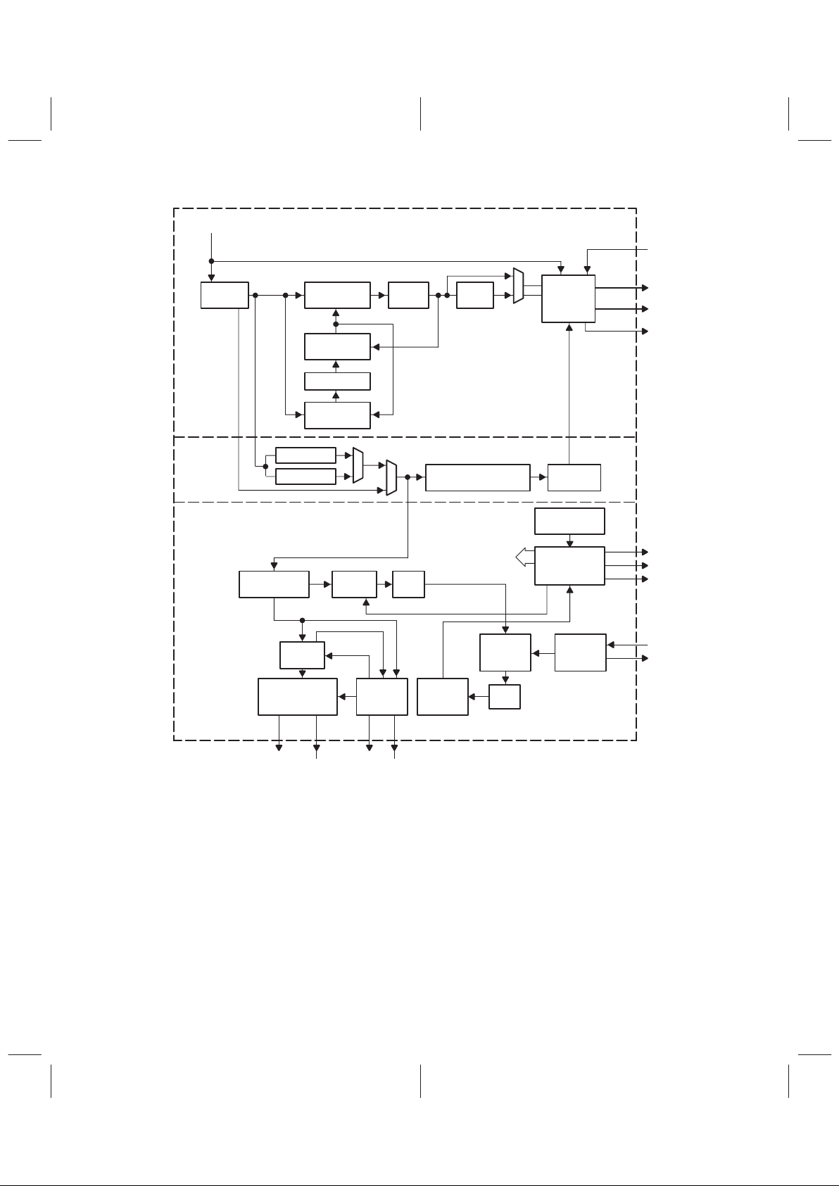
2–2
Input
Interface
Chrominance
Demodulator
Gain
Control
Comb
Filter
Output
Formatter
and
Interface
Digital Control
Oscillator
Loop Filter
Burst Gate
Accumulator
Notch Filter
Comb Filter
Luminance Signal
Processing and Coring
Delay
Adjustment
Lowpass Filter
Sync Detector
Phase
Detector
Loop
Filter
Line-Locked
Clock
PLL
Power-Down
Mode Control
CLOCK
Crystal
Clock
Generator
Digital
Control
Oscillator
DAC
Clock
Generation
Circuit
Vertical
Sync
Processor
Horizontal
Sync
Processor
Counter
CH1
From A/D Converter
CHROMINANCE
LUMINANCE CIRCUITS
SYNCHRONIZATION
OEB
UV (0–7)
Y (0–7)
AVID
PREF
SCLK
PCLK
XTL1
XTL2
HSYN
PALI
(HPLL)
VSYN
FID
(VLK)
Figure 2–2. Digital Video Signal Processing Block Diagram
2.2.1 Y/C Separation
Luma/chroma separation may be done using either 2-line (1–H delay) comb filtering or a chroma trap filter.
Comb filtering is available for both the luminance and the chrominance portion of the data path. The
characteristics of the chroma trap filter are shown in Figures 2–3 and 2–4.
Page 17
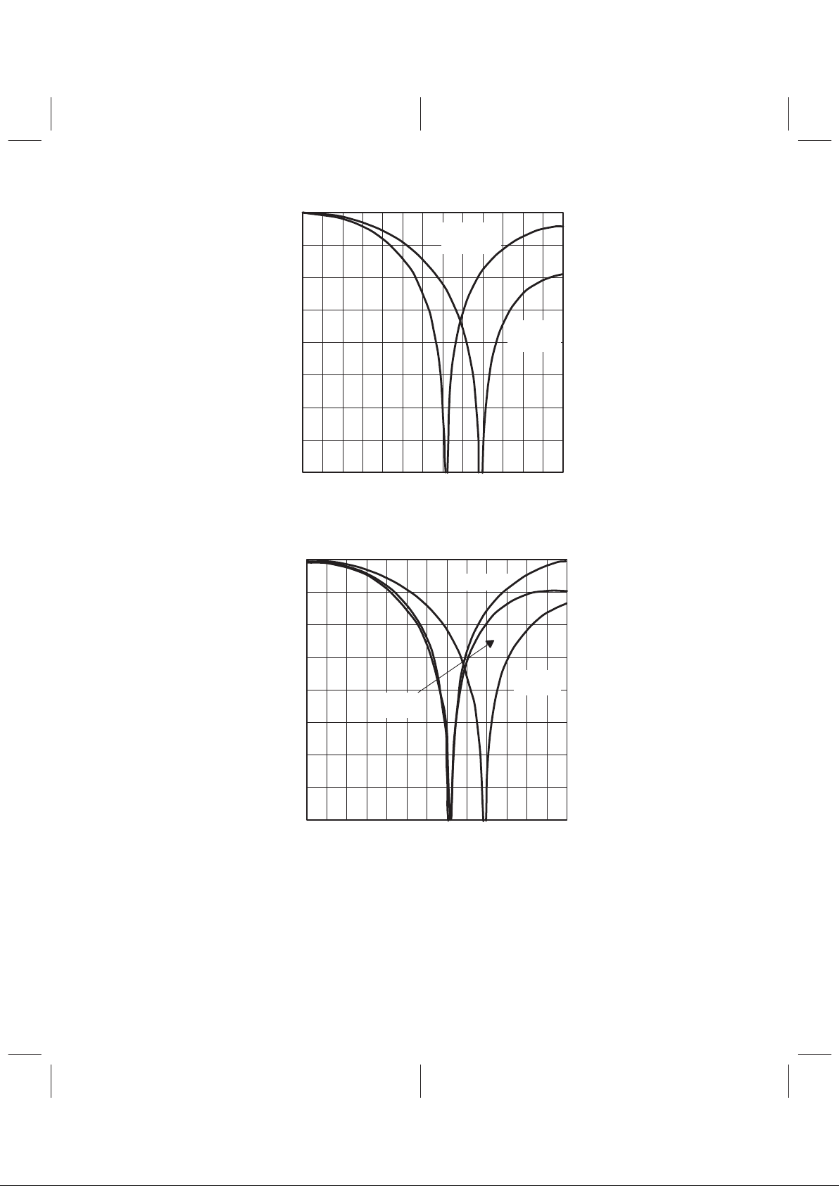
2–3
PAL-B,
D,G,H,I
NTSC,
PAL-M,N
–20
–25
–35
–40
0 0.5 1 1.5 2 2.5 3
Amplitude – dB
–10
–5
f – Frequency – MHz
0
4.5 5 5.5 6.5
–15
–30
3.5
46
Figure 2–3. Chroma T rap Filter Frequency Response for 13.5 MHz Sampling
NTSC,
PAL-M
PAL-N
PAL-B,
D,G,H.I
–20
–30
–35
–40
0 0.5 1 1.5 2 3 3.5
Amplitude – dB
–10
–5
f – Frequency – MHz
0
4.5 5 5.5 6.5
–15
–25
2.5 4 6
Figure 2–4. Chroma T rap Filter Frequency Response for Square-Pixel Sampling
2.2.2 Luminance Processing
The digitized composite video signal from the output of the A/D converter passes through a luminance comb
filter or a chroma trap filter that removes the chrominance signal from the composite signal to generate the
luminance signal. The luminance signal is then fed to the input of luminance signal peaking and coring
circuits. Figure 2–5 illustrates the functions of the luminance data path. High frequency components of the
luminance signal are enhanced further by the peaking filter (edge enhancer). Figures 2–6, 2–7, and 2–8
show the characteristic of the peaking filter at maximum gain. The coring circuit reduces low-level, high
Page 18
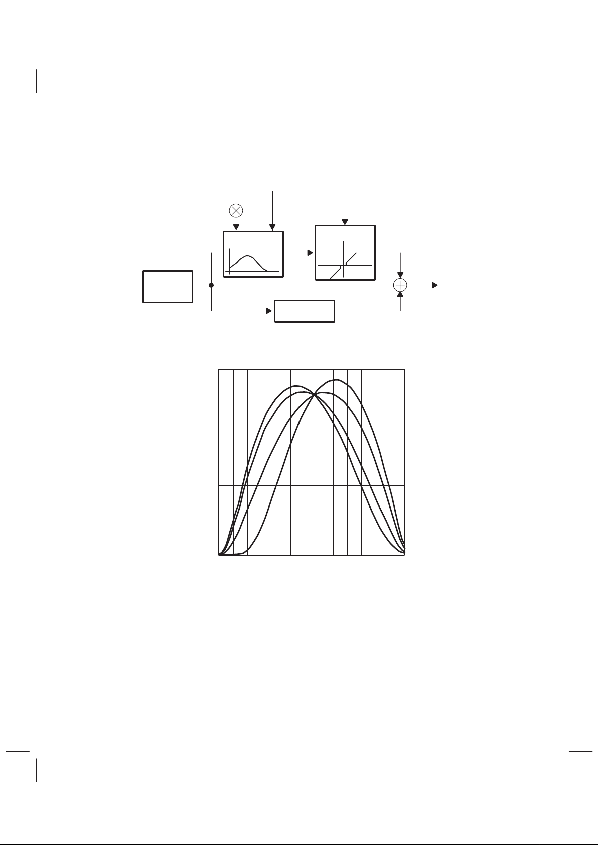
2–4
-frequency noise. Figure 2–9 shows the transfer curve of the coring function. The peaking frequency,
peaking gain, and coring threshold are programmable.
Peaking
Coring
KPK
Peaking
Frequency
Coring
Threshold
COR
Delay
Digital Y
Signal
Aperture
Factor
Y
Figure 2–5. Luminance Edge-Enhancer
8
6
2
0
0 0.5 1 1.5 2 2.5 3
Amplitude – dB
12
14
f – Frequency – MHz
16
3.5 4 5.5 6.5
10
4
4.5 5
6
Figure 2–6. Peaking Filter Response, 13.5 MHz Sampling
Page 19
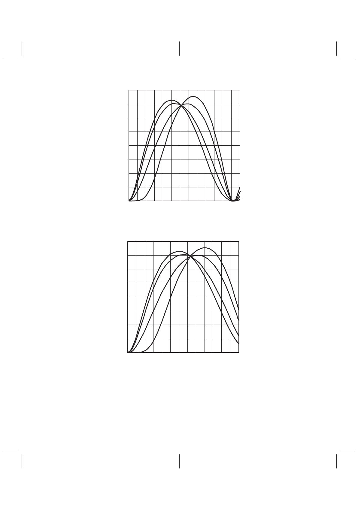
2–5
8
6
2
0
0 0.5 1 1.5 2 3 3.5
Amplitude – dB
12
14
f – Frequency – MHz
16
4.5 5 5.5 6.5
10
4
2.5
46
Figure 2–7. Peaking Filter Response, NTSC AND PAL-M SQUARE PIXEL
8
6
2
0
0 0.5 1 1.5 2 3 3.5
Amplitude – dB
12
14
f – Frequency – MHz
16
4.5 5 5.5 6.5
10
4
2.5
46
Figure 2–8. Peaking Filter Response, PAL Square Pixel
Page 20
2–6
Input Signal
Output Signal
V
I
V
O
Coring Threshold
t
Figure 2–9. Transfer Curve of Coring Circuit
2.2.3 Chrominance Processing
A quadrature demodulator removes the U and V components from the composite signal in composite video
mode. The U/V signals then pass through the gain control stage for chroma saturation adjustment. The U
and V components pass through a comb filter to eliminate cross-chrominance noise. Phase shifting the
digitally-controlled oscillator controls hue. The block includes an automatic color killer (ACK) circuit that
suppresses the chroma output when the color burst of the video signal is weak or not present.
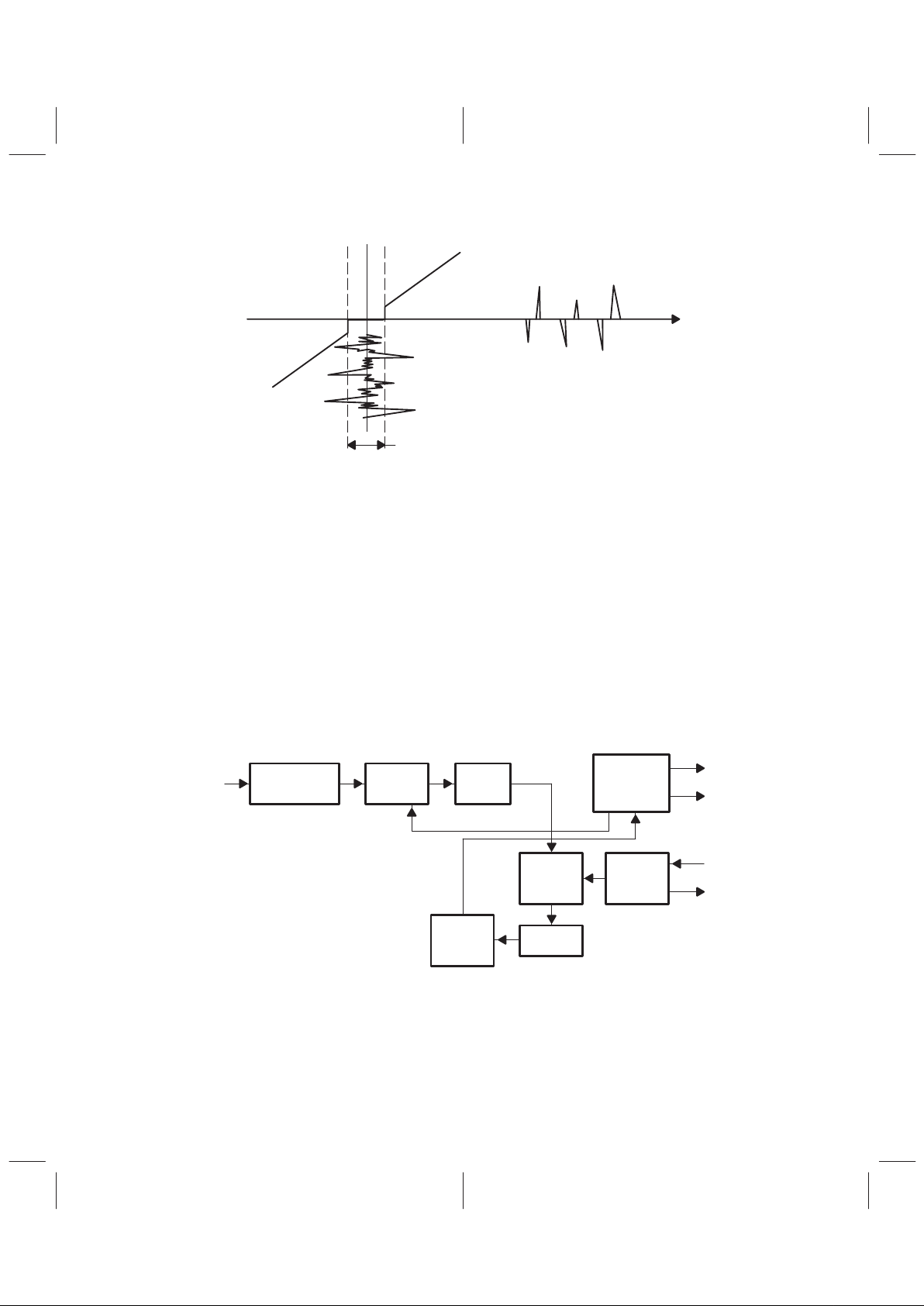
2.2.4 Clock Circuits
An internal line-locked PLL generates the system and pixel clocks. Figure 2–10 shows a simplified clock
circuit diagram. The digital control oscillator (DCO) generates the reference signal for the horizontal PLL.
The DCO outputs a signal that is fed to the D/A converter. The D/A converter outputs a line-locked clock
signal (LCLK). The DCO requires a 26.8 or a 24.576 MHz clock as an input. The input for the DCO may be
connected to terminal XTAL1 or a 26.8 or 24.576 MHz crystal may be connected across terminals XTAL1
and XTAL2. Figure 2–11 shows the various reference clock configurations.
Lowpass Filter
Sync Detector
Phase
Detector
Loop
Filter
Line-Locked
Clock
PLL
Digital
Control
Oscillator
Crystal
Clock
Generator
DAC
Clock
Generator
Circuit
SCLK
PCLK
XTL1
XTL2
Digitized
Video
Figure 2–10. Clock Circuit Diagram
Page 21
2–7
TVP5020
XTAL1
XTAL2
35
36
TVP5020
XTAL1
XTAL2
35
36
26.8 MHz or
24.576 MHz
Crystal
26.8 MHz or
24.576 MHz
TTL Clock
Figure 2–11. Reference Clock Configurations
The TVP5020 generates three signals PCLK, SCLK, and PREF used for clocking data. PCLK is the pixel
clock at the sampling frequency. PCLK can be used for clocking data in the 16-bit 4:2:2 and the 12-bit 4:1:1
output formats. SCLK is at twice the sampling frequency and may be used for clocking data in the 8-bit 4:2:2
and ITU-R BT .656 formats. PREF is used as a clock qualifier with SCLK to clock data in the 16-bit 4:2:2 and
the 12-bit 4:1:1 formats
2.3 Video Output Format
The TVP5020 supports both square-pixel and ITU-R BT .601 sampling formats and multiple output formats:
• 16-bit 4:2:2
• 12-bit 4:1:1
• 8-bit 4:2:2
• ITU-R BT.656
2.3.1 Sampling Frequencies and Patterns
The sampling frequencies that control the number of pixels per line differ depending on the video format and
standards. Table 2–1 shows a summary of the sampling frequencies.
Table 2–1. Summary of the Line Frequencies, Data Rates, and Pixel Counts
STANDARDS
HORIZONTAL
LINE RATE
(kHz)
PIXELS
PER LINE
ACTIVE PIXELS
PER LINE
PCLK (MHz) SCLK (MHz)
NTSC, square-pixel 15.73426 780 640 12.2727 24.54
NTSC, ITU-R BT.601 15.73426 858 720 13.5 27.0
PAL (B,D,G,H,I), square-pixel 15.625 944 768 14.75 29.5
PAL (B,D,G,H,I), ITU-R BT.601 15.625 864 720 13.5 27.0
PAL(M), square-pixel 15.73426 780 640 12.2727 24.54
PAL(M), ITU-R BT.601 15.73426 858 720 13.5 27.0
PAL(N), square-pixel 15.625 944 768 14.75 29.5
PAL(N), ITU-R BT.601 15.625 864 720 13.5 27.0
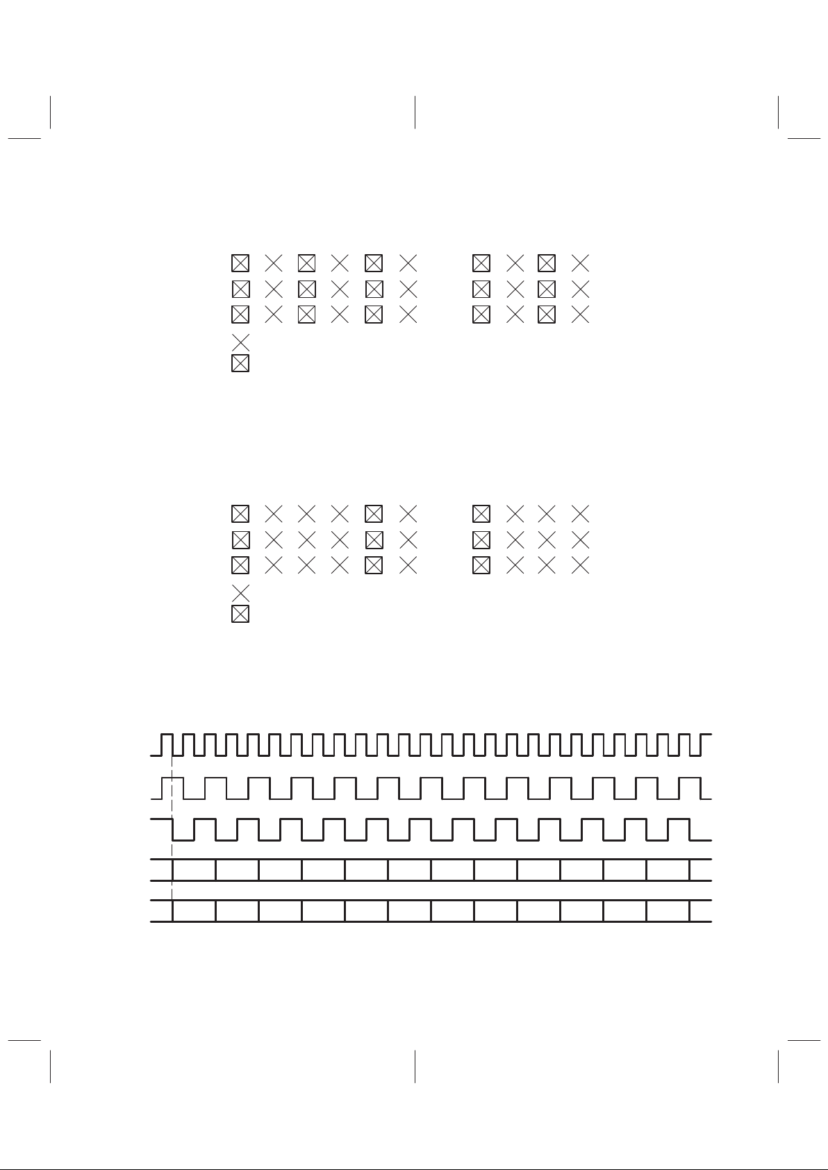
Depending on the output format chosen, The TVP5020 outputs data in the 4:2:2 or 4:1:1 sampling pattern.
The patterns differ in the number of chrominance samples derived from the original samples. For the 4:2:2
pattern, every second sample is both a luminance and a chrominance sample; the remainder are
luminance-only samples. For the 4:1:1 pattern, every fourth sample is both a luminance and a chrominance
sample; the remainder are luminance-only samples.
Page 22
2–8
U2
Y4
V2
U0
Y0
V0
Numbering Shown is for 13.5 MHz Sampling.
= Luminance–Only Sample
Y1U1Y2V1Y3
U358
Y716
V358
Y717
U359
Y718
V359
= Luminance and Chrominance Sample
Y719Y5
Figure 2–12. 4:2:2 Sampling
U1
Y4
V1
U0
Y0
V0
Numbering Shown is for 13.5 MHz Sampling.
= Luminance–Only Sample
Y1 Y2 Y3
U179
Y716
V179
Y717 Y718
= Luminance and Chrominance Sample
Y719Y5
Figure 2–13. 4:1:1 Sampling
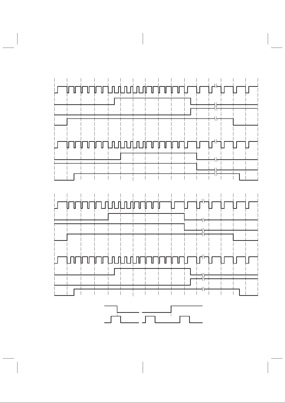
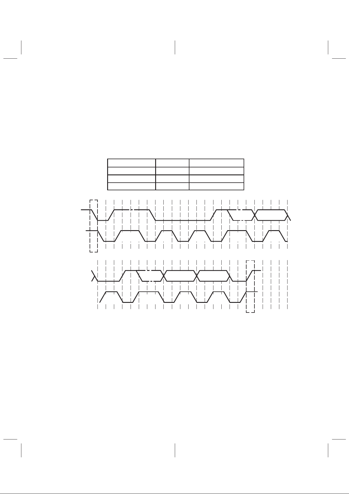
2.3.2 Video Port 16-Bit 4:2:2 Output Format Timing
Y717
V358
PCLK
SCLK
PREF
Y7:0
Y0 Y1 Y2 Y3 Y4 Y5 Y716 Y718 Y719
UV7:0
U0 V0 U1 V1 U2 V2 U358 U359 V359
Numbering Shown is for 13.5 MHz Sampling.
Figure 2–14. 16-Bit 4:2:2 Output Format
Page 23

2–9
2.3.3 Video Port 12-Bit 4:1:1 Output Format Timing
PCLK
SCLK
PREF
Y7:0
Y0 Y1 Y2 Y3 Y4 Y5 Y716 Y717Y717 Y718 Y719
UV5:4
Numbering Shown is for 13.5 MHz Sampling.
UV7:6
U0
(7:6)U0(5:4)U0(3:2)U0(1:0)U1(7:6)U1(5:4)
U179
(7:6)
U179
(5:4)
U179
(3:2)
U179
(1:0)
V0
(7:6)V0(5:4)V0(3:2)V0(1:0)V1(7:6)V1(5:4)
V179
(7:6)
V179
(5:4)
V179
(3:2)
V179
(1:0)
UV3:0 Logic 0
Figure 2–15. 12-bit 4:1:1 Output Format
2.3.4 Video Port 8-Bit 4:2:2 and ITU–R BT.656 Output Format Timing
Y718
SCLK
Y7:0
U0 Y0 V0 Y1 U1 Y2 U359 V359 Y719
Numbering Shown is for 13.5 MHz Sampling.
UV7:0 High Impedance
Figure 2–16. 8-Bit 4:2:2 and ITU-R BT.656 Output Formats
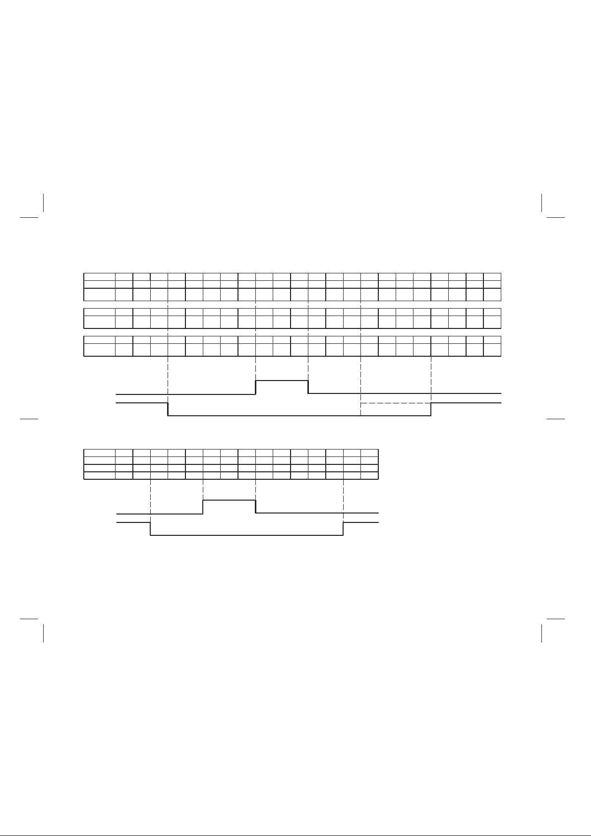
2.4 Synchronization Signals
The TVP5020 generates synchronization signals to accompany the output video data stream. The following
figures show the default timing for the horizontal and vertical sync and associated signals.
Page 24
2–10
Composite
Video–
Odd Field
VSYN
5251 234567891011 212223
FID
GPCL/VBLK
Composite
Video–
Odd Field
VSYN
262 263 264 265 266 267 268 269 270 271 272 273 283 284 285
FID
GPCL/VBLK
Composite
Video–
Odd Field
VSYN
310 311 312 313 314 315 316 317 318 319 320 334 335 336 337
FID
GPCL/VBLK
Composite
Video–
Odd Field
VSYN
622 623 624 625 1 2 3 4 5 6 7 21 22 23 24
FID
GPCL/VBLK
525–Line
625–Line
Note: Line Numbering Conforms to ITU–R BT .470
FID
HSYN
Horizontal Detail (Default HSYN Timing)
Figure 2–17. Vertical Synchronization Signals
Page 25
2–11
8–Bit 4:2:2 Timing With 2x Pixel Clock (SCLK) Reference
16–Bit 4:2:2 Timing With 1x Pixel Clock (PCLK) Reference
AVID
HSYN
AVID
HSYN
1436
NTSC 601
Datastream
Datastream
Datastream
PAL 601
ITU 656
NTSC sqp
ITU 656
PAL sqp
ITU 656
NTSC 601
PAL 601
NTSC sqp
PAL sqp
1437 1438 1439 1440 1441 ... 1471 1472 ... 1599 1560 ... 1711 1712 1713 1714 1715 0 1 2 3
1436 1437 1438 1439 1440 1441 ... 1463 1464 ... 1591 1592 ... 1723 1724 1725 1726 1727 0 1 2 3
Cb
359Y718Cr359Y719
FF 00
...
10 80
...
10 80
...
10 FF 00 00 XX Cb0Y0Cr0Y
1
1276 1277 1278 1279 1280 1281 ... 1323 1324 ... 1451 1452 ... 1555 1556 1557 1558 1559 0 1 2 3
Cb
319Y638Cr319Y639
FF 00
...
10 80
...
10 80
...
10 FF 00 00 XX Cb0Y0Cr0Y
1
1532 1533 1534 1535 1536 1537 ... 1587 1588 ... 1715 1716 ... 1883 1884 1885 1886 1887 0 1123
Cb
383Y766Cr383Y767
FF 00
...
10 80 10 80
... ...
10 FF 00 00 XX Cb0Y0Cr0Y
1
718 719 720 ... 735 736 ... 799 800 ... 855 856 857 0 1
718 719 720 ... 731 732 ... 795 796 ... 861 862 863 0 1
638 639 640 ... 661 662 ... 725 726 ... 777 778 779 0 1
766 767 768 ... 793 794 ... 857 858 ... 941 942 943 0 1
Figure 2–18. Horizontal Synchronization Signals
Page 26
2–12
2.5 I2C/VIP/VMI Host Interface
Communication with the TVP5020 is via an interface that is configurable at power up to support an I2C, VIP ,
or VMI bus host. The host interface accesses status and control registers and retrieves sliced VBI data. The
host interface also initializes the TVP5020’s internal microprocessor.
I2C
Interface
Module
VIP
Interface
Module
VMI
Interface
Module
I/O
MUX
I/O
DMA
BIU
Interface
Module
GLCO, PALI, FID
TVP, CPU
Interface
VDP
Modules
VC0
VC1
VC3
VC0
VC1
VC2
VC3
INTREQ
A0–A1
D0–D7
VC0
VC1
VC2
VC3
INTREQ
Figure 2–19. Host Interface
The host port mode is selected by attaching external pullup and pulldown resistors to the GLCO, PALI, and
FID terminals. The TVP5020 samples the state of the terminals at trailing edge of RSTINB
and configures
the host port accordingly. Table 2–2 shows the pullup/pulldown combinations required to select each of the
host port modes. Figure 2–19 is a block diagram of the host interface showing the mode selection and host
interface terminals, as well as interfaces to the internal microprocessor and VBI data processor.
Table 2–2. Host Port Select
GLCO PALI FID
TERMINALS
2 1 0
I2C Host Port 0 0 1
VIP Host Port 0 1 0
VMI Host Port Mode A 1 0 1
VMI Host Port Mode B 1 1 0
VMI Host Port Mode C 1 1 1
2.6 I2C Interface
The TVP5020 host port interface is configured for I2C operation by attaching external pull-up and pull-down
resisters to the GLCO, PALI, and FID terminals. The following is the combination of resisters required to
select the I
2
C host mode. (1 is pullup and 0 is pulldown)
GLCO PALI FID
TERMINALS
2 1 0
I2C Host Port Enabled 0 0 1
Page 27
2–13
2.6.1 I2C Host Port Select
The I2C standard consists of two signals, serial input/output data (VC1) line and input/output clock line
(VC0), that carry information between the devices connected to the bus. A third signal (VC3) is used for slave
address selection. Although the I
2
C system can be multimastered, the TVP5020 will function as a slave
device only.
Both SDA and SCL are bidirectional lines that connect to a positive supply voltage via a pullup resistor. When
the bus is free, both lines are high.
The slave address select terminal (VC3) enables the use of two TVP5020 devices tied to the same I
2
C bus.
Table 2–3 summarizes the terminal functions of the I
2
C mode host interface.
Table 2–3. I
2
C Host Port Terminal Description
SIGNAL TYPE DESCRIPTION
VC3 (I2CA) I Slave address selection
VC0 (SCL) I/O (OD) Input/output clock line
VC1 (SDA) I/O (OD) Input/output data line
NOTE: OD = Open drain
1–7
Address
8
RW
9
ACK
1–7
Data
8
Data
9
ACK
1–7
Data
8
Data
9
ACK
P
S
VC1
(SDA)
VC0
(SCL)
Start Condition
VC0
(SCL)
Stop
12C Data Transfer
Figure 2–20. I2C Data Transfer Example
Data transfer rate on the bus is up to 400 kbits/s. The number of interfaces connected to the bus is dependent
on the bus capacitance limit of 400 pF. The data on the SDA line must be stable during the high period of
the clock. The high or low state of the data line can only change with the clock signal on the SCL line being
low.
• When transferring multiple bytes during one read or write operation, the internal subaddress is
not automatically incremented.
• A high to low transition on the SDA line while the SCL is high indicates a start condition.
• A low to high transition on the SDA line while the SCL is high indicates a stop condition
• Acknowledge is signalled by SDA low during the ninth SCL high.
• Not-acknowledge is signalled by SDA high during the ninth SCL high.
Every byte placed on the SDA line must be 8 bits long. The number of bytes that can be transferred is
unrestricted. An acknowledge bit follows each byte. If the slave can not receive another complete byte of
data until it has performed another function, it holds the clock line (SCL) low. An SCL low forces the master
Page 28

2–14
into a wait state. Data transfer continues when the slave is ready for another byte of data and releases the
clock line (SCL).
Data transfer with acknowledge is necessary. The master generates an acknowledge related clock pulse.
The master releases the SDA line high during the acknowledge clock pulse. The slave pulls down the SDA
line during the acknowledge clock pulse so that it remains stable low during the high period of this clock
pulse.
When a slave does not acknowledge the slave address, the data line is left high. The master then generates
a stop condition to abort the transfer.
If a slave acknowledges the slave address, but some time later in the transfer cannot receive any more data
bytes, the master again aborts the transfer. The slave indicates a not ready condition by generating the not
acknowledge. The slave leaves the data line high and the master generates the stop condition.
If a master-receiver is involved in a transfer, it indicates the end of data to the slave-transmitter by not
generating an acknowledge on the last byte that was clocked out of the slave. The slave-transmitter must
release the data line to allow the master to generate a stop or repeated start condition.
2.6.2 I2C Write Operation
Data transfers occur using the following illustrated formats.
The I
2
C master initiates a write operation to the TVP5020 by generating a start condition followed by the
TVP5020’s I
2
C address (101110X). The address is in MSB first bit order followed by a 0 to indicate a write
cycle. After receiving a TVP5020 acknowledge, the I2C master sends a subaddress of the register or the
block of registers where it will write. Following the subaddress is one or more bytes of data, with MSB first.
The TVP5020 acknowledges the receipt of each byte upon completion of each transfer. The I
2
C master ends
a write operation by generating a stop condition.
The X in the address of the TVP5020 is 0 when the I
2
CA terminal is low and the X is 1 when the I2CA is high.
If the read or write cycle contains more than one byte, the internal subaddress does not increment
automatically.
0
I2C Start (Master) S
7 6 5 4 3 2 1 0
I2C General address (Master) 1 0 1 1 1 0 X 0
9
I2C Acknowledge (Slave) A
7 6 5 4 3 2 1 0
I2C Write register address (Master) Addr Addr Addr Addr Addr Addr Addr Addr
9
I2C Acknowledge (Slave) A
7 6 5 4 3 2 1 0
I2C Write data (Master) Data Data Data Data Data Data Data Data
9
I2C Acknowledge (Slave) A
0
I2C Stop (Master) P
Page 29

2–15
2.6.3 I2C Read Operation
The read operation has two phases, the address phase and the data phase. In the address phase, the I2C
master initiates a write operation to the TVP5020 by generating a start condition followed by the TVP5020’s
I
2
C address (101110X). The address is in MSB first bit order followed by a 0 to indicate a write cycle. After
receiving a TVP5020 acknowledge, the I
2
C master sends a subaddress of the register or the block of
registers where it will read. The TVP5020 acknowledges the receipt of the address. The I
2
C master ends
the address phase by generating a stop condition. During the data phase, the I
2
C master initiates a read
operation to the TVP5020 by generating a start condition followed by the TVP5020’s I
2
C address (1011 10X).
The address is in MSB first bit order followed by a 1 to indicate a read cycle. After receiving a TVP5020
acknowledge, the TVP5020 transfers a data byte to the master. The I
2
C master acknowledges the receipt
of each byte upon completion of each transfer. After the TVP5020 transfers the last byte, the I
2
C master ends
the read operation by generating a not acknowledge followed by a stop condition.
Read Address Phase
0
I2C Start (Master) S
7 6 5 4 3 2 1 0
I2C General address (Master) 1 0 1 1 1 0 X 0
9
I2C Acknowledge (Slave) A
7 6 5 4 3 2 1 0
I2C Write register address (Master) Addr Addr Addr Addr Addr Addr Addr Addr
9
I2C Acknowledge (Slave) A
0
I2C Stop (Master) P
Read Data Phase
0
I2C Start (Master) S
7 6 5 4 3 2 1 0
I2C General address (Master) 1 0 1 1 1 0 X 1
9
I2C Acknowledge (Slave) A
7 6 5 4 3 2 1 0
I2C Read data (Slave) Data Data Data Data Data Data Data Data
9
I2C Acknowledge (Master) /A
0
I2C Stop (Master) P
Page 30

2–16
2.6.4 I2C Microcode Write Operation
Data written during the microcode write operation will be written to the TVP5020 program RAM. During the
write cycle the microprocessor resets and points to location zero in the program and remains reset. Upon
completion of the write operation, the microprocessor requires a restart operation. T o perform a clear-reset
requires writing into the 7F register to clear reset and resume microprocessor function. (The 7F register
requires no specific data written into the register, any data will resume microprocessor function).
0
I2C Start (Master) S
7 6 5 4 3 2 1 0
I2C General address (Master) 1 0 1 1 1 0 X 0
9
I2C Acknowledge (Slave) A
7 6 5 4 3 2 1 0
I2C Write register address (Master) 0 1 1 1 1 1 1 0
9
I2C Acknowledge (Slave) A
7 6 5 4 3 2 1 0
I2C Write data (Master) Data Data Data Data Data Data Data Data
9
I2C Acknowledge (Slave) A
0
I2C Stop (Master) P
Page 31

2–17
Microprocessor CLEAR Reset
0
I2C Start (Master) S
7 6 5 4 3 2 1 0
I2C General address (Master) 1 0 1 1 1 0 X 0
9
I2C Acknowledge (Slave) A
7 6 5 4 3 2 1 0
I2C Write register address (Master) 0 1 1 1 1 1 1 1
9
I2C Acknowledge (Slave) A
7 6 5 4 3 2 1 0
I2C Write data (Master) Data Data Data Data Data Data Data Data
Any Data Written to 7F Will Start the Microprocessor
9
I2C Acknowledge (Slave) A
0
I2C Stop (Master) P
2.6.5 I2C Microcode Read Operation
Data read during the microcode read operation will be read from the TVP5020 Program RAM. During the
read cycle the microprocessor resets and points to location zero in the program and remains reset. Upon
completion of the read operation, the microprocessor requires a restart operation. T o perform a clear–reset
requires writing into the 7F register to clear reset and resume microprocessor function. (The 7F register
requires no specific data written into the register, any data will resume microprocessor function).
Read Address Phase
0
I2C Start (Master) S
7 6 5 4 3 2 1 0
I2C General address (Master) 1 0 1 1 1 0 X 0
9
I2C Acknowledge (Slave) A
7 6 5 4 3 2 1 0
I2C Read register address (Master) 1 0 0 0 1 1 1 0
9
I2C Acknowledge (Slave) A
Page 32

2–18
0
I2C Stop (Master) P
Read Data Phase
0
I2C Start (Master) S
7 6 5 4 3 2 1 0
I2C General address (Master) 1 0 1 1 1 0 X 1
7
I2C Acknowledge (Slave) A
7 6 5 4 3 2 1 0
I2C Read data (Slave) Data Data Data Data Data Data Data Data
7
I2C Acknowledge (Master) A
NOTE: Repeat byte read sequence for N–1 bytes where N is the total number of bytes to be read
7 6 5 4 3 2 1 0
I2C read data (Slave) Data Data Data Data Data Data Data Data
9
I2C Acknowledge (Master) /A
0
I2C Stop (Master) P
Microprocessor CLEAR Reset
0
I2C Start (Master) S
7 6 5 4 3 2 1 0
I2C General address (Master) 1 0 1 1 1 0 X 0
9
I2C Acknowledge (Slave) A
7 6 5 4 3 2 1 0
I2C Write register address (Master) 0 1 1 1 1 1 1 1
Write to FIFO address=7F
9
I2C Acknowledge (Slave) A
Page 33

2–19
7 6 5 4 3 2 1 0
I2C Write data (Master) Data Data Data Data Data Data Data Data
NOTE: Any data written to 7F will start the microprocessor .
9
I2C Acknowledge (Slave) A
0
I2C Stop (Master) P
2.7 VIP Host Interface Port
The TVP5020 host interface is configured for video interface port (VIP) by attaching external pullup and
pulldown resisters to the GLCO, PALI, and FID terminals. The following is the combination of resisters
required to select the VIP host mode. (1 is pullup and 0 is pulldown)
GLCO PALI FID
TERMINALS
2 1 0
VIP host port enabled 0 1 0
The VIP is a standard interface, conforming to the video interface port (VIP) specification Version 1.1. The
interface is between a video enabled graphics device and one or more video devices. The video port of VIP
transports various types of real-time signal streams. Signal names in parentheses denote the signal name
referenced in VIP specification.Host port transfers require five terminals, VC3, VC0, VC1, VC2, INTREQ.
Page 34

2–20
2.7.1 VIP Host Port Terminal Description
Table 2–4. VIP Host Port Terminal Description
SIGNAL TYPE DESCRIPTION
VC3 (VIPCLK) I VIP Host clock (25 MHz – 33 MHz)
VC0 VC1 (HAD[0:1]) I/O Host address/data bus
VC0 = (HAD_0)
VC1 = (HAD_1)
VC2 (HCTL) I/O (OD) Host control: This includes the symbolic signals of VFRAME, DTACK, and VSTOP
INTREQ (VIRQ#) O (OD) Interrupt request. Shared signal with VDP
VC3 (VIPCLK) is the host port clock, operating from 25 MHz–33 MHz. VIPCLK can come from any source.
VC0 and VC1 (HAD[0:1]) is a two-wire bus that transfers commands, addresses, and data between master
and slave devices.
VC2 (HCTL) is a shared control terminal. The master drives it to initiate and terminate data transfers. The
slave drives it to terminate and add wait states to data transfers. Because VC2 is a shared control signal,
special attention must be given to its generation to avoid bus conflicts.
INTREQ is a normally open drain pin that signals interrupts to the host controller. Using the interrupt
configuration register at subaddress C2, this terminal can be configured as a conventional CMOS I/O buffer
(non-open drain). Conflict is possible if multiple devices are connected to the INTREQ signal when it is
configured in non-open drain mode.
2.7.2 VIP Phases
Command Phase Address Phase DC Retry Phase Data Phase TAPh
Command Address
7:6 5:4 3:2 1:0 7:6 5:4 3:2 1:0
Don’t
Care
Don’t
Care
Don’t
Care
Don’t
Care
Don’t
Care
7:6 5:4 3:2 1:0 7:6
Data
Decode Phase Allows
Slave to Decode
Address
Bus Turn Around Phase
Cmd
Master Drive HCTL High
to Start Transfer
Slave Drives DTACK to
Signal Data is Ready for
the Next Phase
GUI Must Drive This
Low Dring Idle
Master Drives Low
During Idle
Master 3-states
VC2 (HCTL) Floats
VSTOP Can Drive Low to
Terminate The Transfer. If Terminated
There Will Be No Data Phase
Slave Drives High if
Not Terminated in
Cycle
Slave 3-states
VC2 (HCTL) Remains High
FRAME and or VSTOP Drives
Low to Terminate The Transfer
Slave May Drive DTACK Low For
The Next Byte. It is Irrelevant as
Transfer is Already Terminated
VC3
(VIPCLK)
VC0 (HAD0)
VC1 (HAD1)
VC2
(HCTL)
Zero Wait State
Figure 2–21. VIP Transfer Example
Page 35

2–21
Table 2–5. VIP Host Port Phase Description
PHASE EXPLANATION
Command All host port transfers start with a command phase. The 8-bit command/address byte is multiplexed onto
VC0 and VC1 (HAD[1:0]) during the command phase. The command byte selects between devices, read,
and write cycles, register or FIFO transfers, and contains the most significant four bits of the register
address.
Address During register transfers the command phase is followed by the address extension phase. The least
significant 8-bits of the VIP register address are multiplexed onto VC0 and VC1 (HAD[1:0]) during the
address extension phase. This phase is not present during FIFO transfers.
Decode Following the command or command/address phase(s), the bus requires one clock delay to allow slave
devices to decode the address and determine if they are able to respond within the 1 wait phase
requirement for active operation.
Retry The four clock cycles immediately following the decode phase constitute the retry phase. During the retry
phase, the slave indicates its desire to terminate the operation without transferring any data (retry), add a
wait phase or transfer the first byte of data. When the slave asserts VSTOP , the transfer ends with the retry
phase. When the slave neither terminates the transfer nor accepts the byte, the retry phase is followed by
a wait phase.
Wait During the second cycle of a decode, retry or wait phase, the slave indicates its ability to transfer the next
byte of data by driving VC2 (HCTL) low. When the slave does not drive VC2 (HCTL) low and the transfer is
not terminated, the current phase is followed by a wait phase. During wait phases, the current owner
(master for writes, slave for reads) continues to drive the HAD bus, but no data is transferred. The slave is
allowed to add one wait phase per byte to register accesses without compromising system timing.
Additional wait phases are not prevented but overall system reliability may be compromised.
Data When VC2 (HCTL) is removed during cycle 1 of a retry, wait or data phase, a data phase follows the
current phase. The bus transfers data between master and slave devices during data phases. The data is
multiplexed onto VC0 and VC1 (HAD[1:0]).
T
A
Immediately following the last transfer phase of a read transfer, the slave requires a one cycle delay giving
time to 3-state the VC0 and VC1 (HAD) bus. The master is free to begin a new bus transfer , driving VC0
and VC1 (HAD) and VC2 (HCTL) immediately following the TA phase.
Table 2–6. Condensed Table Command/Address
COMMAND Cmd/Addr REGISTER ADDRESS DATA COMMENT
[7:4] [3:0] [7:0] [7:0]
01 1 0 0000 00000000 thru 11111111 dddddddd VIP configuration registers
01 0/1 0 0001 00000000 thru 11111111 dddddddd General TVP registers
01 1 0 0010 00000000 thru 11111111 xxxxxxxx No latency read access 1 phase
01 1 0 0011 addr as prev. written ddddddd No latency read access 2 phase
01 1 1 0000 No addr phase xxx0/1xxx0/1 FIFO status 0 read
01 1 1 0001 No addr phase xxxxxx11 FIFO status 1 read
01 1 1 0100 No addr phase dddddddd FIFO VBI data read
2.7.3 Command Byte
During the command byte phase, the hardware control line (VC2) will transition high and the hardware
address lines (VC0 and VC1) transmits the command byte from the host to the TVP5020. The command
byte determines the nature of the data transfer and the affected TVP5020 address space.
7 6 5 4 3 2 1 0
Command DEVSEL1 (0) DEVSEL0 (1) R/W F/R A11 A10 A9 A8
Page 36

2–22
Command Byte Bit Description
NAME DESCRIPTION
DEVSEL1:0 Device select. Always 01 for TVP5020
R/W 1=Read 0=Write
F/R 1=FIFO 0=Register access
A11:8 Address bus upper 4 bits
For register accesses:
0000=VIP specific configuration registers
0001=General TVP5020 registers
0010=No latency read access phase 1
0011=No latency read access phase 2
For FIFO accesses:
0000=FIFO status 0
0001=FIFO status 1
0100=VBI FIFO
2.7.3.1 Access Latency and Wait States
VIP accesses to registers or the VBI FIFO require the TVP5020 to insert one or more wait states into the
access sequence. For register accesses, the wait states may total as much as 64 µs. All writes will release
the host port immediately, but internal wait states will continue to be generated until the operation completes.
Any access attempts to the host port while the write operation is not completed will cause the slave to
terminate the operator. Reads (except for no-latency reads) will hold the host port until completion.
Wait
Command
Address DC Wait Wait Last Wait
Wait States Can Last Up to 64 µs
Data TAWait Last Wait
Wait States Can Last Up to 64 µs
Data
VC3
VC1
VC0
VC2
VC3
VC2
VC1
VC0
Figure 2–22. Functional Timing Reading From TVP (Example)
Page 37

2–23
Command Address DC Wait Data
VC3
VC2
Wait
TAWait Data
VC3
VC2
WaitWait Wait
Wait States Can Last Up to 64 µs
VC1
VC0
VC1
VC0
Figure 2–23. Functional Timing Writing to TVP (Example)
DCCommand
VC3
VC2
WaitWait Wait
TAData Data
VC3
VC2
WaitWait Wait
VC1
VC0
VC1
VC0
Figure 2–24. Functional Timing Reading From FIFO (Example)
Page 38

2–24
DCCommand
VC3
VC0
VC1
VC2
WaitAddress Command
Slave Termination
Figure 2–25. Functional Timing Example of Slave Termination
VIP Configuration Register:
The TVP5020 supports VIP configuration registers that are accessible only in the VIP host mode.
COMMAND PHASE ADDRESS PHASE
DATA PHASE
(from TVP5020)
7 6 5 4 3 2 1 0 7 6 5 4 3 2 1 0 7 6 5 4 3 2 1 0
VIP Config. Register read 0 1 1 0 0 0 0 0 A A A A A A A A D D D D D D D D
General TVP5020 Registers:
The bulk of the TVP5020 register space consists of status and control registers that are available to the I2C,
VIP, and VMI host modes.
COMMAND PHASE ADDRESS PHASE
DATA PHASE
(from TVP5020)
7 6 5 4 3 2 1 0 7 6 5 4 3 2 1 0 7 6 5 4 3 2 1 0
General TVP register read 0 1 1 0 0 0 0 1 A A A A A A A A D D D D D D D D
COMMAND PHASE ADDRESS PHASE
DATA PHASE
(to TVP5020)
7 6 5 4 3 2 1 0 7 6 5 4 3 2 1 0 7 6 5 4 3 2 1 0
General TVP register write 0 1 0 0 0 0 0 1 A A A A A A A A D D D D D D D D
2.7.3.2 No-latency Read
No-latency read eliminates the extended wait states of normal read operations. No latency read consists
of two zero-wait state phases separated by an idle period during which the host may perform other
operations. The first phase identifies the register address to be read. This will be stored in an intermediate
data buffer . The current data in the intermediate data buf fer is immediately read out. This information is to
be ignored because it is invalid data.
Following the completion of the first phase, the host must wait for at least 64 µs to ensure that the data
requested in the first phase is stored in the intermediate data buffer. The host initiates the second phase
of the read by reading the data from the intermediate data buffer .
No Latency Read Phase 1:
COMMAND PHASE ADDRESS PHASE
DATA PHASE
(from TVP5020)
7 6 5 4 3 2 1 0 7 6 5 4 3 2 1 0 7 6 5 4 3 2 1 0
No latency read
phase 1
0 1 1 0 0 0 1 0 A A A A A A A A du du du du du du du du
Page 39

2–25
No Latency Read Phase 2:
COMMAND PHASE ADDRESS PHASE
DATA PHASE
(to TVP5020)
7 6 5 4 3 2 1 0 7 6 5 4 3 2 1 0 7 6 5 4 3 2 1 0
No Latency Read Phase 2 0 1 1 0 0 0 1 1 A A A A A A A A D D D D D D D D
2.7.3.3 FIFO Status 0 Register
FIFO status 0 register returns two bits that report status and six unused bits.
7 6 5 4 3 2 1 0
FIFO Status 0 Undefined Undefined Undefined DREQA Undefined Undefined Undefined VIRQ
DREQA: DMA request for FIFO A. This bit is the same as the teletext threshold bit (bit 1 of the interrupt status
register at VIP address1C0).
VIRQ: this bit returns the status of the INTREQ terminal. Reading this register does not clear this terminal.
COMMAND PHASE DATA PHASE
7 6 5 4 3 2 1 0 7 6 5 4 3 2 1 0
FIFO Status 0 0 1 1 1 0 0 0 0 d d d 0/1 d d d 0/1
There is no address associated with reading the FIFO status 0 register.
2.7.3.4 FIFO Status 1 Register
The FIFO status 1 register returns two bits that report status and six unused bits.
7 6 5 4 3 2 1 0
FIFO Status 1 Undefined Undefined Undefined Undefined Undefined Undefined R/W PRESENT
R/W This bit identifies the VBI FIFO is read–only and is always set to 1.
PRESENT This bit indicates the VBI FIFO is present and is always set to 1.
COMMAND PHASE DATA PHASE
7 6 5 4 3 2 1 0 7 6 5 4 3 2 1 0
FIFO Status 1 0 1 1 1 0 0 0 1 dc dc dc dc dc dc 1 1
There is no address associated with reading the FIFO status 1 register.
2.7.3.5 VBI FIFO
The VBI FIFO stores sliced VBI data. The data may be read from the FIFO at an average rate of one data
byte per three cycles (1 data cycle and 2 wait cycles) when the VIPCLK is at maximum speed.
COMMAND PHASE DATA PHASE
7 6 5 4 3 2 1 0 7 6 5 4 3 2 1 0
FIFO VBI data read 0 1 1 1 0 1 0 0 D D D D D D D D
There is no address associated with reading the VBI FIFO.
Page 40

2–26
2.7.4 VIP Microcode Write Operation
Data is written to the TVP5020 program RAM during the microcode write operation. During the write cycle,
the microprocessor resets and points to location zero in the program and remains reset. Following the first
data phase, the data phase is repeated until all microcode is written. The microprocessor requires a
clear-reset operation upon completion of the write operation. The host performs the reset by writing into the
7F register to clear reset and resume microprocessor function. (There is no specific data to be written into
the 7F register; any data will resume microprocessor function).
COMMAND PHASE ADDRESS PHASE
DATA PHASE
(to TVP5020)
7 6 5 4 3 2 1 0 7 6 5 4 3 2 1 0 7 6 5 4 3 2 1 0
Microcode write 0 1 0 0 0 0 0 1 0 1 1 1 1 1 1 0 D D D D D D D D
The data phase is repeated to the end of the microcode.
COMMAND PHASE ADDRESS PHASE
DATA PHASE
(to TVP5020)
7 6 5 4 3 2 1 0 7 6 5 4 3 2 1 0 7 6 5 4 3 2 1 0
Clear reset 0 1 0 0 0 0 0 1 0 1 1 1 1 1 1 1 X X X X X X X X
2.7.5 VIP Microcode Read Operation
Data is read from the TVP5020 program RAM during the microcode read operation. During the read cycle,
the microprocessor resets and points to location zero in the program and remains reset. Following the first
data phase, the data phase is repeated until all microcode is read. The microprocessor requires a clear-reset
operation upon completion of the read operation. The host performs the reset by writing into the 7F register
to clear reset and resume microprocessor function. (There is no specific data to be written into the 7F
register; any data will resume microprocessor function)
.
COMMAND PHASE ADDRESS PHASE
DATA PHASE
(from TVP5020)
7 6 5 4 3 2 1 0 7 6 5 4 3 2 1 0 7 6 5 4 3 2 1 0
Microcode read 0 1 1 0 0 0 0 1 1 0 0 0 1 1 1 0 D D D D D D D D
The data phase is repeated to the end of the microcode.
COMMAND PHASE ADDRESS PHASE
DATA PHASE
(to TVP5020)
7 6 5 4 3 2 1 0 7 6 5 4 3 2 1 0 7 6 5 4 3 2 1 0
Clear reset 0 1 0 0 0 0 0 1 0 1 1 1 1 1 1 1 X X X X X X X X
2.8 Video Module Interface (VMI) Host Interface
The VMI host port interface is configurable for three possible modes of operation. The mode of operation
is determined by attaching pullup or pulldown resistors to the GLCO, PALI, and FID terminals. Table 2–7
shows the various modes. (0=pulldown and 1=pullup)
Table 2–7. VMI Host Port Select
GLCO PALI FID
TERMINALS
2 1 0
VMI Host Port Mode A 1 0 1
VMI Host Port Mode B 1 1 0
VMI Host Port Mode C 1 1 1
Page 41

2–27
VMI modes A and B are from the Video Electronics Standards Association (VESA) video module interface
(VMI) proposal version 1.4. Mode C is designed to conform to the interface requirements of the IBM
PowerPC 403GC. Table 2–8 summarizes the terminal functions of the VMI mode host interface.
Table 2–8. VMI Host Port Terminal Definitions
SIGNAL
VMI SIGNAL
NAME
TYPE DESCRIPTION
VC3 CS I Chip select - modes A, B, and C
VC0 DTACK – mode A
READY – mode B
O (see below)
Data acknowledge – mode A
Data ready – modes B and C
VC1 R/W – mode A
WR – mode B
I
Read/write – modes A and C
Write strobe – mode B
VC2 DS – mode A
RD – mode B
I
Data strobe – mode A and C
Read strobe – mode B
A1:A0 HA[1:0] I Address bus from host
D7:D0 HD[7:0] I/O Input/output data bus from host
INTREQ INTREQ O (nominal open drain) Interrupt request
INTREQ is a nominally open drain terminal that signals interrupts to the host controller. The interrupt
configuration register at subaddress C2 can configure this terminal as a conventional CMOS I/O buffer
(non-open drain). Conflict is possible if INTREQ is connected to multiple devices and INTREQ is not
configured in the open drain mode.
VC0 (DTACK/READY) is in the high impedance state when VC3 is not asserted.
2.9 Host Port – Mode A Timing
Host port mode A has a bus interface that accommodates the Motorola type of control signals. The diagram
below shows the timing of the mode A signals. The host initiates the cycle when VC2 transitions low. The
target responds by pulling VC0 low to indicate it is receiving the data or that the requested data is present
on the bus. The host completes its cycle by pulling VC2 high. Once the host completes its cycle, the target
pulls VC0 high. The host may change VC1, A[1:0], and Din[7:0] as soon as it receives VC0.
ÎÎÎÎ
ÎÎÎÎ
ÎÎÎÎ
ООООООООО
205 ns Max 85 ns Min
20 ns Min
Read Data
Write Data
VC2 (DS)
VC1 (R/W
)
A (0–1)
D IN (0–7)
D OUT (0–7)
VC0 (DTACK)
Figure 2–26. VMI Host Port Mode A Timing
Page 42

2–28
2.10 Host Port – Mode B Timing
Host port mode B has a bus interface that accommodates the Intel type of control signals. The diagram
below shows the timing of the mode B signals. The host presents the address and chip select when the
command (VC1 or VC2) transitions low. The VMI module pulls VC0 low until the read or write operation is
complete. VC1 and VC2 cannot both be low while VC3 is low.
125 ns Max
85 ns Min
20 ns Min
Write Data
Read Data
VC2 (RD
)
VC1 (WR
)
VC3 (CS
)
A (0–1)
D (0–7)
D (0–7)
C0 (READY)
Figure 2–27. Host Port Mode B Timing
2.11 Host Port – Mode C Timing (PPC)
Host port mode C has a bus interface that accommodates the IBM PowerPC 403GC type of control signals.
The Figure 2–21 shows the timing of the mode C signals. Mode C is similar to mode A (Motorola) except
that a ready signal is used instead of VC0.
125 ns Max 85 ns Min
20 ns Min
Read Data
Write Data
VC2 (DS)
VC1 (R/W
)
A (0–1)
D (0–7)
D (0–7)
VC0 (READY)
Figure 2–28. Host Port Mode C Timing
Page 43

2–29
2.11.1 VMI Register Mapping
The VMI module contains only four registers that are accessible by the host. The address register holds an
indirect address for internal register access. When the host accesses the data register, the VMI module
reads or writes the internal register selected by the indirect address register.
Two other registers are provided for direct access. The FIFO register provides direct access to the VBI FIFO
and the second direct access register is the status/interrupt register. This register contains the state of the
interrupt sources.
A[1:0]
00 Address register
01 Data register
10 FIFO
11 Status register
Figure 2–29. VMI Address Register Map
Normally, read or write operations require two accesses. To read the FIFO register , set A[1:0] to 10(binary)
and perform a read cycle. The FIFO read data will be placed on the D[7:0] bus. To read/write the
status/interrupt register, set A[1:0] to 1 1(binary) and perform a read/write cycle. The read/write will be muxed
appropriately to/from the external data bus.
Indirect Register Read/Write:
All VMI accesses except for the VBI FIFO and the status/interrupt register require a two-step operation. T o
access an indirect register, write the internal address to the VMI address register. The first step requires
setting A[1:0] to 00 and performing a write cycle with D[7:0] equaling the indirect address. To write to an
indirect register, the second step is to write the data to VMI address 01. To read an indirect register, the
second step is to read the the requested data from address 01.
Read the indirect register
STEP 1 A1 A0 D7 D6 D5 D4 D3 D2 D1 D0
Write register address 0 0 Register address
STEP 2 A1 A0 D7 D6 D5 D4 D3 D2 D1 D0
Read register data 0 1 Data from register
Write to the indirect register
STEP 1 A1 A0 D7 D6 D5 D4 D3 D2 D1 D0
Write register address 0 0 Register address
STEP 2 A1 A0 D7 D6 D5 D4 D3 D2 D1 D0
Write register data 0 1 Data to register
Latency:
VMI access to indirect addresses 00–8F requires special consideration due to response latencies of up to
64 µs for these addresses. Latency occurs between steps one and two for a read operation and following
step two of a write operation. T o avoid violating the VMI cycle time requirements, the host can poll the cycle
complete bit in the VMI status register following step one for a read or step two for a write. Alternatively, the
cycle complete enable bit in the interrupt enable register (indirect address C1) can be set to generate an
interrupt for the host when access is complete.
VMI access to indirect addresses 90-CF occur with minimal latency . Interrupts will not be generated for the
completion of access cycles to these addresses.
Page 44

2–30
VBI FIFO:
The VBI FIFO containing sliced VBI data is directly readable by the VMI host.
A1 A0 D7 D6 D5 D4 D3 D2 D1 D0
Read VBI FIFO 1 0 Data from FIFO
Status/Interrupt Register:
The status/interrupt register provides the host with information containing the source of an interrupt. After
an interrupt condition is set, the condition can be reset by writing a one to the appropriate bit in the
status/interrupt register.
A1 A0 D7 D6 D5 D4 D3 D2 D1 D0
Access status/interrupt register 1 1 Data to/from status/interrupt register
2.11.2 VMI Microcode Write Operation
Data written to indirect register 7E will be written to the TVP5020 program RAM. During the address write
cycle the microprocessor resets and points to location zero in the program and remains reset. The
microprocessor requires a clear-reset operation upon completion of the write operation. The host performs
the reset by writing into the 7F register to clear reset and resume microprocessor function. (There is no
specific data to be written into the 7F register; any data will resume microprocessor function).
T o avoid violating VMI cycle time requirements during microcode write operation, the host can poll the cycle
complete bit in the VMI status register after writing each byte of data to the VMI data register. Alternatively,
the cycle complete enable bit in the interrupt enable register (indirect address C1) can be set to generate
an interrupt for the host when a write operation is complete.
A1 A0 D7 D6 D5 D4 D3 D2 D1 D0
Write microcode
Register address
0 0 0 1 1 1 1 1 1 0
A1 A0 D7 D6 D5 D4 D3 D2 D1 D0
Write microcode
Register data
Write microcode
Register Data
Write microcode
Register data
0
0
0
1
1
1
First byte of microcode data
(Wait for cycle complete status or interrupt)
Second Byte of microcode data
(Wait for cycle complete status or interrupt)
Last byte of microcode data
(Wait for cycle complete status or interrupt)
A1 A0 D7 D6 D5 D4 D3 D2 D1 D0
Write clear reset
Register address
0 0 0 1 1 1 1 1 1 1
A1 A0 D7 D6 D5 D4 D3 D2 D1 D0
Write clear reset
Dummy data
0 1 X X X X X X X X
Page 45

2–31
2.11.3 VMI Microcode Read Operation
Data read from indirect register 8E will be read from the TVP5020 program RAM. During the read cycle, the
microprocessor resets, points to location zero in the program, and remains reset. The microprocessor
requires a clear-reset operation upon completion of the read operation. The host performs the reset by
writing into the 7F register to clear reset and resume microprocessor function. (There is no specific data
to be written into the 7F register; any data will resume microprocessor function)
.
To avoid violating VMI cycle time requirements during the microcode read operation, the host can poll the
cycle complete bit in the VMI status register. This polling shoud be done following the address load cycle
(for indirect register 8Eh). Alternatively, the cycle complete enable bit in the interrupt enable register (indirect
address C1) can be set to generate an interrupt for the host when data from a read cycle is unavailable.
STEP 1 A1 A0 D7 D6 D5 D4 D3 D2 D1 D0
Write microcode
Register address
0 0 1 0 0 0 1 1 1 0
STEP 2 A1 A0 D7 D6 D5 D4 D3 D2 D1 D0
Read register data 0 1 Data Data Data Data Data Data Data Data
Note: Must readdress for each read of incremental data
STEP 1 A1 A0 D7 D6 D5 D4 D3 D2 D1 D0
Write microcode
Register address
0 0 1 0 0 0 1 1 1 0
STEP 2 A1 A0 D7 D6 D5 D4 D3 D2 D1 D0
Read register data 0 1 Data Data Data Data Data Data Data dData
A1 A0 D7 D6 D5 D4 D3 D2 D1 D0
Write clear reset
Register address
0 0 0 1 1 1 1 1 1 1
A1 A0 D7 D6 D5 D4 D3 D2 D1 D0
Write clear reset
Dummy data
0 1 Data Data Data Data Data Data Data Data
2.12 Genlock Control
The frequency control word of the internal color subcarrier digital control oscillator (DCO) and the subcarrier
phase reset bit are transmitted via the GLCO terminal. The frequency control word is a 23-bit binary number.
The frequency of the DCO can be calculated from the following equation:
F
dco
+
F
ctrl
2
23
×
F
sclk
Where F
dco
is the frequency of the DCO, F
ctrl
is the 23-bit DCO frequency control, and F
sclk
is the frequency
of the SCLK.
The last bit (bit 0) of the DCO frequency control is always 0.
A write of 1 to bit 4 of the chrominance control register at host port subaddress 1Ah causes the subcarrier
DCO phase reset bit to be sent on the next scan line on GLCO. The active low reset bit occurs 8 SCLKs
after the transmission of the last bit of DCO frequency control. Upon the transmission of the reset bit, the
phase of the TVP5020 internal subcarrier DCO is reset to zero.
A genlocking slave device connected to the GLCO terminal can use the information on GLCO to synchronize
its internal color DCO to achieve clean line and color lock.
Page 46

2–32
Figure 2–30 shows the timing of GLCO.
SCLK
GLCO
23-Bit frequency controlStart bit DCO reset
MSB LSB
>128 SCLK
1
SCLK
1
SCLK
8 SCLK23 SCLK
Figure 2–30. GLCO Timing
2.13 VBI Data Processor
The TVP5020 VBI data processor slices, parses, and performs error checking on teletext data contained
in the vertical blanking interval or during active lines. T eletext formats supported are North American Basic
Teletext Specification (NABTS) equivalent to ITU-R BT.653 system C, and World System Teletext (WST)
equivalent to ITU-R BT .653 system B. Data is stored in an internal FIFO and may be read via the host port
or transmitted as ancillary data in the digital video stream in BT.656 mode. The VBI data FIFO holds up to
14 lines of NABTS or 11 lines of WST data. Interrupts generated by the VBI data processor are configurable
to enable host synchronization for retrieval of full-field teletext data.
VBI data processor may also slice closed caption data and store it in two registers accessible via the host
port.
2.13.1 Teletext Data Byte Order
Table 2–9 shows the order in which teletext data is read from the FIFO.
Table 2–9. Teletext Byte Order
BYTE
NUMBER
NABTS – 525 OR 625
LINE SYSTEM
WST – 525 LINE SYSTEM WST – 625 LINE SYSTEM
1 Video line [7:0] Video Line [7:0] Video Line [7:0]
2 00, Hamming error, parity error,
LPC error, match #2, match #1,
video line [8]
00, Hamming error, parity error ,
LPC error, match #2, match #1,
video line [8]
00, Hamming error, parity error ,
LPC error, match #2, match #1,
video line [8]
3 Packet address 1 Magazine Magazine
4 Packet address 2 Row address Row address
5 Packet address 3 Data byte 1 Data byte 1
6 Continuity index Data byte 2 Data byte 2
7 Packet structure Data byte 3 Data byte 3
8 Data block 1 Data byte 4 Data byte 4
9 Data block 2 Data byte 5 Data byte 5
10 Data block 3 Data byte 6 Data byte 6
11 Data block 4 Data byte 7 Data byte 7
12 Data block 5 Data byte 8 Data byte 8
Page 47

2–33
Table 2–9. Teletext Byte Order (Continued)
BYTE
NUMBER
NABTS – 525 OR 625
LINE SYSTEM
WST – 525 LINE SYSTEM WST – 625 LINE SYSTEM
13 Data block 6 Data byte 9 Data byte 9
14 Data block 7 Data byte 10 Data byte 10
15 Data block 8 Data byte 11 Data byte 11
16 Data block 9 Data byte 12 Data byte 12
17 Data block 10 Data byte 13 Data byte 13
18 Data block 11 Data byte 14 Data byte 14
19 Data block 12 Data byte 15 Data byte 15
20 Data block 13 Data byte 16 Data byte 16
21 Data block 14 Data byte 17 Data byte 17
22 Data block 15 Data byte 18 Data byte 18
23 Data block 16 Data byte 19 Data byte 19
24 Data block 17 Data byte 20 Data byte 20
25 Data block 18 Data byte 21 Data byte 21
26 Data block 19 Data byte 22 Data byte 22
27 Data block 20 Data byte 23 Data byte 23
28 Data block 21 Data byte 24 Data byte 24
29 Data block 22 Data byte 25 Data byte 25
30 Data block 23 Data byte 26 Data byte 26
31 Data block 24 Data byte 27 Data byte 27
32 Data block 25 Data byte 28 Data byte 28
33 Data block 26 Data byte 29 Data byte 29
34 Data block 27/suffix Data byte 30 Data byte 30
35 Data block 28/suffix Data byte 31 Data byte 31
36 Padding byte
†
Data byte 32 Data byte 32
37 Data byte 33
38 Data byte 34
39 Data byte 35
40 Data byte 36
41 Data byte 37
42 Data byte 38
43 Data byte 39
44 Data byte 40
†
The padding byte is used to ensure an even number of writes. This byte does not contain any useful information. The
read pointer automatically advances past this byte so the user does not have to read the padding byte.
2.13.2 Teletext as Ancillary Data in Video Stream
Sliced teletext data can be output as ancillary data in the video stream in ITU-R BT .656 mode. Teletext data
is output on the Y7:0 pins during the horizontal blanking period following the line that the data was retrieved.
Dummy ancillary data blocks with special timing header information are inserted during certain horizontal
blanking periods to provide data synchronization information. Tables 2–10 through 2–13 show the format
and sequence of the ancillary data inserted into the video stream.
Page 48

2–34
Table 2–10. NABTS 525/625-Line Ancillary Data Sequence
BYTE
NO.
MSB
7
6 5 4 3 2 1
LSB
0
DESCRIPTION
1 0 0 0 0 0 0 0 0
2 1 1 1 1 1 1 1 1
Ancillary data preamble
3 1 1 1 1 1 1 1 1
4 NEP EP 0 1 0 DID2 DID1 DID0 Data ID
5 1 0 0 0 0 0 0 0 Secondary data ID
6 1 0 0 0 1 0 0 1 Number of 32-bit data words
7 Video line number 7:0
8 0 0
Hamming
error
Parity
error
LPC
error
Match#2Match#1Video
line 8
Internal data ID
9 Packet address 1 Data byte
10 Packet address 2 Data byte
11 Packet address 3 Data byte
12 Continuity index Data byte
13 Packet structure Data byte
14 Teletext data 1 Data byte
15 Teletext data 2 Data byte
39 Teletext data 26 Data byte
40 Teletext data 27/suf fix Data byte
41 Teletext data 27/suf fix Data byte
42 Checksum Checksum
43 1 0 0 0 0 0 0 0 Fill byte
44 1 0 0 0 0 0 0 0 Fill byte
Page 49

2–35
Table 2–11. WST 525-Line Ancillary Data Sequence
BYTE
NO.
MSB
7
6 5 4 3 2 1
LSB
0
DESCRIPTION
1 0 0 0 0 0 0 0 0
2 1 1 1 1 1 1 1 1
Ancillary data preamble
3 1 1 1 1 1 1 1 1
4 NEP EP 0 1 0 DID2 DID1 DID0 Data ID
5 1 0 0 0 0 0 0 0 Secondary data ID
6 1 0 0 0 1 0 0 1 Number of 32-bit data words
7 Video line number 7:0
8 0 0
Hamming
error
Parity
error
LPC
error
Match#2Match#1Video
line 8
Internal data ID
9 Magazine Data byte
10 Row address Data byte
11 Teletext data 1 Data byte
12 Teletext data 2 Data byte
Data byte
42 Teletext data 32 Data byte
43 NEP EP Checksum Checksum
44 1 0 0 0 0 0 0 0 Fill byte
Table 2–12. WST 625-Line Ancillary Data Sequence
BYTE
NO.
MSB
7
6 5 4 3 2 1
LSB
0
DESCRIPTION
1 0 0 0 0 0 0 0 0
2 1 1 1 1 1 1 1 1
Ancillary data preamble
3 1 1 1 1 1 1 1 1
4 NEP EP 0 1 0 DID2 DID1 DID0 Data ID
5 1 0 0 0 0 0 0 0 Secondary data ID
6 0 1 0 0 1 0 1 1 Number of 32-bit data words
7 Video line number 7:0
8 0 0
Hamming
error
Parity
error
LPC
error
Match#2Match#1Video
line 8
Internal data ID
9 Magazine Data byte
10 Row address Data byte
11 Teletext data 1 Data byte
12 Teletext data 2 Data byte
Data byte
50 Teletext data 40 Data byte
51 NEP EP Checksum Checksum
52 1 0 0 0 0 0 0 0 Fill byte
Page 50

2–36
Table 2–13. Dummy Timing Ancillary Data Sequence
BYTE
NO.
MSB
7
6 5 4 3 2 1
LSB
0
DESCRIPTION
1 0 0 0 0 0 0 0 0
2 1 1 1 1 1 1 1 1
Ancillary data preamble
3 1 1 1 1 1 1 1 1
4 NEP EP 0 1 0 DID2 DID1 DID0 Data ID
5 1 0 0 0 0 0 0 0 Secondary data ID
6 1 0 0 0 0 0 0 0 Number of 32-bit data words
In the tables above, EP is even parity on the lower 6 bits and NEP is negated even parity. The checksum
for teletext data blocks is the 8 LSB’s of the sum of the data bytes. The data ID byte provides timing
information. Table 2–14 shows the possible values of the data ID byte and their meanings.
Table 2–14. Ancillary Data ID
DATA ID EVENT IN SOURCE STREAM DATA TYPE
50 Start of first, odd field Dummy timing block
91 Sliced data of lines 1–23 of first field VBI data
92 End of nominal VBI of first field, line 23 Dummy timing block
53 Sliced data of line 24 to end of first field Full field teletext data
94 Start of second, even field Dummy timing block
55 Sliced data of lines 1–23 of second field VBI data
56 End of nominal VBI of second field, line 23 Dummy timing block
97 Sliced data of line 24 to end of second field Full field teletext data
A dummy timing block will be inserted into the video stream during the horizontal blanking period following
line 23 of each field. If teletext data is available from line 23 it will be inserted into the video stream prior to
the dummy timing block.
2.14 Reset
Reset is initiated at power up or any time the RSTINB terminal is brought low. Table 2–15 describes the
status of the terminals on the TVP5020 during and immediately after reset. Following a powerup reset, the
host downloads microcode to the program memory of the TVP5020 for use by the internal microprocessor.
Table 2–15. Power-Up Reset Sequence
SIGNAL NAMES DURING RESET AFTER RESET
RSTINB, OEB, EXT_DATA_8 In In
GLCO, PALI, FID, GPCL In Out
UV[7:0] In High-impedance
SCLK, PCLK, PREF High-impedance Out
Y[7:0], HSYN, VSYN, AVID High-impedance High-impedance
Host interface terminals: VC0, VC1, VC2, VC3, INTREQ, A1:0, D7:0 High-impedance Active
Signals take their reset values during power up and anytime the RSTINB terminal is low.
The active state of the host interface terminals may be input, output, or input/output depending on the host
mode selected during reset.
Page 51

2–37
2.15 Internal Control Registers
Table 2–16 shows the summary of the TVP5020 registers. The detailed programming information of each
register is described in the following sections. For writable registers, the reserved bits must be written with
a 0.
Table 2–16. Registers Summary
REGISTER FUNCTION VIP VMI I2C R/W
Vendor ID 000 – 001 NA NA R
Device ID 002 – 003 NA NA R
Subsystem vendor ID 004 – 005 NA NA R
Subsystem device ID 006 – 007 NA NA R
Reserved 008 – 00B NA NA
Revision ID 00C – 00D NA NA R
Reserved 00E – 0FF NA NA
Analog input source selection 100 00 ← 00 00 W
Analog channel controls 101 00 ← 01 01 W
Operation mode controls 102 00 ← 02 02 W
Miscellaneous controls 103 00 ← 03 03 W
Reserved 104 – 105 00 ← 04 – 05 04 – 5
Color killer threshold control 106 00 ← 06 06 W
Luminance processing controls–#1 107 00 ← 07 07 W
Luminance processing controls–#2 108 00 ← 08 08 W
Brightness control 109 00 ← 09 09 W
Color saturation control 10A 00 ← 0A 0A W
Hue control 10B 00 ← 0B 0B W
Contrast control 10C 00 ← 0C 0C W
Outputs and data rate select 10D 00 ← 0D 0D W
Reserved 10E – 115 00 ← 0E – 15 0E – 15
Horizontal sync start NTSC 116 00 ← 16 16 W
Horizontal sync start PAL 117 00 ← 17 17 W
Vertical blanking start 118 00 ← 18 18 W
Vertical blanking stop 119 00 ← 19 19 W
Chrominance control 11A 00 ← 1A 1A W
Reserved 11B – 11F 00 ← 1B – 1F 1B – 1F
Digital channel selection 120 00 ← 20 20 W
Reserved 121 – 17D 00 ← 21 – 7D 21 – 7D
Program RAM write 17E 00 ← 7E 7E W
Microprocessor reset clear 17F 00 ← 7F 7F W
Firmware version 180 00 ← 80 80 R
Status #1 181 00 ← 81 81 R
Status #2 182 00 ← 82 82 R
AGC gain 183 00 ← 83 83 R
Page 52

2–38
Table 2–16. Registers Summary (Continued)
REGISTER FUNCTION VIP VMI I2C R/W
Reserved 184 – 18D 00 ← 84 – 8D 84 – 8D
Program RAM read 18E 00 ← 8E 8E R
Reserved 18F 00 ← 8F 8F
TXF filter #1 parameters (R/W) 190 – 194 00 ← 90 – 94 90 – 94 R/W
TXF filter #2 parameters (R/W) 195 – 199 00 ← 95 – 99 95 – 99 R/W
TXF error filtering enable 19A 00 ← 9A 9A R/W
TXF transaction processing enables 19B 00 ← 9B 9B R/W
Reserved 19C – 19F 00 ← 9C – 9F 9C – 9F
TTX control register 1A0 00 ← A0 A0 R/W
Line enable register 1A1 – 1A2 00 ← A1 – A2 A1 – A2 R/W
Sync pattern register 1A3 00 ← A3 A3 R/W
Reserved 1A4 – AF 00 ← A4 – AF A4 – AF
Teletext FIFO 1B0 00 ← B0 B0 R
Closed caption data 1B1 – 1B2 00 ← B1 – B2 B1 – B2 R
Buffer status 1B3 00 ← B3 B3 R
Interrupt threshold 1B4 00 ← B4 B4 R/W
Interrupt line number 1B5 00 ← B5 B5 R/W
FIFO control 1B6 00 ← B6 B6 R/W
Reserved 1B7 – 1BF 00 ← B7 – BF B7 – BF R/W
Interrupt status register 1C0 00 ← C0 C0 R/W
Interrupt enable register 1C1 00 ← C1 C1 R/W
Interrupt configuration register 1C2 00 ← C2 C2 R/W
Reserved 1C3 – 1FF 00 ← C3 – FF C3 – FF
No–Latency read access 1 2xx R
No–Latency read access 2 3xx R
FIFO 10 R
Interrupt status register 11 R/W
2.15.1 Register Definitions
2.15.2 Vendor ID
VIP address 000–001
VMI address NA
I2C address NA
Address 7 6 5 4 3 2 1 0
000 0 1 0 0 1 1 0 0
001 0 0 0 1 0 0 0 0
This field identifies the manufacturer of the device. Address 001 is the MSB. This field is a constant of 104C.
Page 53

2–39
2.15.3 Device ID
VIP address 002–003
VMI address NA
I2C address NA
Address 7 6 5 4 3 2 1 0
002 0 0 1 0 0 0 0 0
003 0 1 0 1 0 0 0 1
This field identifies the particular device. Address 003 is the MSB. This field is a constant of 5120
2.15.4 Subsystem Vendor ID
VIP address 004–005
VMI address NA
I2C address NA
Address 7 6 5 4 3 2 1 0
004 Loaded from UV pins on powerup reset
005 1 1 1 1 1 1 1 1
This field identifies the subsystem manufacturer (e.g., the board manufacturer). Address 005 is the MSB.
This field is a constant of FF. The value of the LSB is set at the device power up or reset by sampling the
state of UV[7:0] terminals. The UV[7:0] terminals may be tied to pullup or pulldown resistors to determine
a fixed value for the subsystem vendor ID.
2.15.5 Subsystem Device ID
VIP address 006–007
VMI address NA
I2C address NA
Address 7 6 5 4 3 2 1 0
006 1 1 1 1 1 1 1 1
007 1 1 1 1 1 1 1 1
This field identifies the subsystem device. Address 007 is the MSB. This field is a constant of FFFF.
2.15.6 Subsystem Revision ID
VIP address 00C–00D
VMI address NA
I2C address NA
Address 7 6 5 4 3 2 1 0
00C 0 0 0 0 0 0 0 0
00D 0 0 0 0 0 0 0 1
This identifies the device hardware revision. Address 00D is the MSB. This field is a constant of 0100.
Page 54

2–40
2.15.7 Analog Input Source Selection
VIP address 100
VMI address 00
I2C address 00
7 6 5 4 3 2 1 0
Reserved Channel 1 source selection Reserved
Channel 1 source selection:
0 = VI1A selected (default)
1 = VI1B selected
ADC1
0
1
Channel 1
Register 00, Bit 1
0
1
Register 20, Bit 0
0
1
Register 20, Bit 2
External A/D (UV Pins)
0
1
Luma/Composite
Datapath
Chroma Datapath
0
1
Register 0D, Bit 4
Y
UV
VI1A
VI1B
Figure 2–31. Video Input Source Selection
Table 2–17. Analog Channel and Video Mode Selection
ADDRESS 00 ADDRESS 20
INPUT(s) SELECTED
BIT 1 BIT 1 BIT 0
Composite 1A 0 0 0
1B 1 0 0
Page 55

2–41
2.15.8 Analog Channel Controls
VIP address 101
VMI address 01
I2C address 01
7 6 5 4 3 2 1 0
Reserved Reserved Automatic clamping control. Channel 1 Automatic gain control
Automatic clamping control, channel 1:
00 = Reserved
01 = Automatic clamping enabled (default)
10 = Reserved
11 = Clamping level frozen
Automatic gain control:
00 = Reserved
01 = AGC enabled using luma input as the reference (default)
10 = Reserved
11 = AGC frozen
Page 56

2–42
2.15.9 Operation Mode Controls
VIP address 102
VMI address 02
I2C address 02
7 6 5 4 3 2 1 0
External A/D width TV/VCR mode Reserved Disable color PLL Reserved Power down mode
External A/D width:
00 = 8-bit external A/D
01 = 9-bit external A/D terminal OEB is the LSB of the 9-bit input data
10 = 10-bit external A/D terminal GPCL is the LSB of the 10–bit input data, and terminal OEB is the
next–to–LSB (default)
11 = Reserved
An external A/D converter can be used to provide up to 10-bit data directly to the digital data path. These
bits set the width of the external data path. External A/D access is enabled by register 20, bit 2. See
Figure 2–31 and register 20.
TV/VCR mode:
00 = Automatic mode determined by the internal detection circuit (default)
01 = Reserved
10 = VCR (nonstandard video) mode
1 1 = TV (standard video) mode
With automatic detection enabled, unstable or nonstandard syncs on input video will force the device into
VCR (nonstandard) mode. This turns off the luminance and chrominance comb filters and turns on the
chroma trap filter.
Disable color PLL:
0 = Normal operation (default)
1 = Force color PLL increment and genlock (GLCO) serial output to zero
Power down mode:
0 = Normal operation (default)
1 = Power down mode
Page 57

2–43
2.15.10 Miscellaneous Controls
VIP address 103
VMI address 03
I2C address 03
7 6 5 4 3 2 1 0
Terminal GPCL
function select
Terminals PALI and
FID function select
YUV out-
put enable
HSYN, VSYN,
AVID enable
Reserved Vertical
blanking on/off
Clock enable
Terminal GPCL function select:
00 = Terminal GPCL is logic 0 output (default)
01 = Terminal GPCL is logic 1 output
10 = Terminal GPCL is vertical blank output
11 = Terminal GPCL is external sync lock control input
When GPCL is configured as a vertical blank output, the vertical blanking on/off bit is used to activate the
output.
When GPCL is configured as a sync lock control, it can be used to force the internal PLLs to their normal
settings. This causes all clocks and synchronization signals to assume nominal values. The sync lock
control input is active high.
Terminals PALI and FID function select:
0 = Terminal PALI outputs PAL indicator signal and terminal FID outputs field ID signal (default)
1 = Terminal PALI outputs horizontal lock indicator (HLK) and terminal FID outputs vertical lock
indicator (VLK)
YUV output enable:
0 = YUV high impedance (default)
1 = YUV active
Y[7:0] and UV[7:0] terminals are controlled by this bit, the YUV enable bit in register C2, and the OEB
terminal.
Table 2–18. YUV Output Controls
OEB
Pin
Reg 03,
Bit 4
Rec C2,
Bit 2
YUV OUTPUT
0 x 0 High impedance
0 0 x High impedance
0 1 1 Active
1 x x High impedance
Page 58

2–44
Horizontal sync (HSYN),Vertical sync (VSYN), and Active video indicator (AVID) outputs enable:
0 = HSYN, VSYN, and AVID disabled, (high impedance state) (default)
1 = HSYN, VSYN, and AVID active
Vertical blanking on/off control:
0 = Vertical blanking off. Output is logic zero (default)
1 = Vertical blanking on
This bit is functional if GCPL is configured to output vertical blank.
Clock enable:
0 = SCLK and PCLK outputs are high impedance
1 = SCLK and PCLK outputs are enabled (default)
2.15.11 Color Killer Threshold Control
VIP address 106
VMI address 06
I2C address 06
7 6 5 4 3 2 1 0
Reserved Automatic color killer Color killer threshold
Automatic color killer:
00 = Automatic mode (default)
01 = Reserved
10 = Color killer enabled. The UV terminals are forced to a zero color state
11 = Color killer disabled
Color killer threshold (ref. 0 dB = nominal burst amplitude):
11111= – 30 dB
10000= – 24 dB (default)
00000= –18 dB
Page 59

2–45
2.15.12 Luminance Processing Control 1
VIP address 107
VMI address 07
I2C address 07
7 6 5 4 3 2 1 0
Reserved Pedestal Reserved Luma bypass during vertical
blank
Luminance signal delay with respect
to chrominance signal
Pedestal:
0 = 7.5 IRE pedestal is present on the analog video input (default)
1 = Pedestal is not present on the analog video input
Luminance bypass mode during vertical blanking:
0 = No (default)
1 = Yes
When the luminance bypass is enabled, the luminance comb and notch filters are turned off and the
chrominance components of the output video are sent to a zero color state. Luminance bypass will occur
for the duration of the vertical blanking as defined by registers 18 and 19. This feature may be used to prevent
distortion of test and data signals present during the vertical blanking interval.
Luma signal delay with respect to chroma signal in pixel clock increments (range –8 to 7 pixel clocks):
1111= –8 pixel clocks delay
1011= –4 pixel clocks delay
1000= –1 pixel clocks delay
0000= 0 pixel clocks delay (default)
0011= 3 pixel clocks delay
0111= 7 pixel clocks delay
Page 60

2–46
2.15.13 Luminance Processing Control 2
VIP address 108
VMI address 08
I2C address 08
7 6 5 4 3 2 1 0
Luma filter select Coring threshold Peaking gain Peaking frequency
Luminance filter select:
00 = Automatic select (default)
01 = Reserved
10 = Chroma trap (notch filter)
11 = Comb filter
With automatic select enabled, unstable or nonstandard syncs on input video will force selection of the
chroma trap (notch) filter. For PAL imputs, automatic select will always selct the chroma trap filter.
Coring threshold:
00 = Coring off (default)
01 = ±1 LSB
10 = ±2 LSB
11 = ±3 LSB
Peaking gain:
00 = Peaking disabled (default)
01 = 6 dB
10 = 12 dB
1 1 = 18 dB
Peaking frequency:
Square-pixel sampling rate:
NTSC PAL PAL M PAL N
00 = 3.8 MHz 4.5 MHz 3.8 MHz 4.5 MHz (default)
01 = 3.4 MHz 4.1 MHz 3.4 MHz 4.1 MHz
10 = 2.5 MHz 3.0 MHz 2.5 MHz 3.0 MHz
11 = 2.7 MHz 3.2 MHz 2.7 MHz 3.2 MHz
ITU-R BT.601 sampling rate:
ALL STANDARDS
00 = 4.1 MHz (default)
01 = 3.7 MHz
10 = 2.8 MHz
11 = 3.0 MHz
Page 61

2–47
2.15.14 Brightness Control
VIP address 109
VMI address 09
I2C address 09
7 6 5 4 3 2 1 0
Brightness control
Brightness:
11111111= 255 (bright)
10000000= 128 (default)
00000000= 0 (dark)
2.15.15 Color Saturation Control
VIP address 10A
VMI address 0A
I2C address 0A
7 6 5 4 3 2 1 0
Saturation control
Saturation:
11111111= 255 (maximum)
10000000= 128 (default)
00000000= 0 (no color)
2.15.16 Hue Control
This register (Sub-address = 0Bh) sets the hue of the color signal.
VIP address 10B
VMI address 0B
I2C address 0B
7 6 5 4 3 2 1 0
Hue control
Hue:
01111111= 180 degrees
00000000= 0 degrees (default)
10000000= –180 degrees
Page 62

2–48
2.15.17 Contrast Control
VIP address 10C
VMI address 0C
I2C address 0C
7 6 5 4 3 2 1 0
Contrast control
Contrast:
11111111= 255 (maximum contrast)
10000000= 128 (default)
00000000= 0 (minimum contrast)
2.15.18 Outputs and Data Rates Select
VIP address 10D
VMI address 0D
I2C address 0D
7 6 5 4 3 2 1 0
Reserved YUV output code range UV code format YUV data path bypass Reserved YUV output format
YUV output code range:
0 = ITU-R BT.601 coding range (Y ranges from 16 to 235, UV components range from 16 to 240)
(default)
1 = Extended coding range (Y, and UV components range from 1 to 254)
UV code format:
0 = Offset binary code (2’s complement + 128) (default)
1 = Straight binary code (2’s complement)
YUV data path bypass:
0 = Normal operation (default)
1 = Y terminals connected to channel 1 A/D output, UV terminals connected to channel 2 A/D output
YUV output format:
000 = 16-bit 4:2:2 (default)
001 = Reserved
010 = 12-bit 4:1:1
011 = Reserved
100 = 8-bit 4:2:2
101 = Reserved
1 10 = Reserved
1 11 = 8-bit ITU-R BT. 656 with embedded syncs
Page 63

2–49
2.15.19 Horizontal Sync (HSYN) Start
VIP address 116–117
VMI address 16–17
I2C address 16–17
Address 7 6 5 4 3 2 1 0
16 HSYN start for NTSC
17 HSYN start for PAL
HSYN start:
11111111= –127 × 4 pixel clocks
11111110= –126 × 4 pixel clocks
11111101= –125 × 4 pixel clocks
10000000= 0 pixel clocks (default)
01111111= 1 × 4 pixel clocks
01111110= 2 × 4 pixel clocks
00000000= 128 × 4 pixel clocks
2.15.20 Vertical Blanking Start
VIP address 118
VMI address 18
I2C address 18
7 6 5 4 3 2 1 0
VBLK start
VBLK start:
01111111= 127 lines after start of vertical blanking interval
00000001= 1 line after start of vertical blanking interval
00000000= Same time as start of vertical blanking interval (default)
01111111= 1 line before start of vertical blanking interval
10000000= 128 lines before start of vertical blanking interval
Vertical blanking is adjustable with respect to the standard vertical blanking intervals as shown in
Figure 2–17. The setting in this register determines the timing of the GPCL signal when it is configured to
output vertical blank (see register 03). The setting in this register is also used to determine the duration of
the luma bypass function (see register 07).
Page 64

2–50
2.15.21 Vertical Blanking VBLK Stop
VIP address 119
VMI address 19
I2C address 19
7 6 5 4 3 2 1 0
VBLK end
VBLK start:
01111111= 127 lines after end of vertical blanking interval
00000001= 1 line after end of vertical blanking interval
00000000= Same time as end of vertical blanking interval (default)
11111111= 1 line before end of vertical blanking interval
10000000= 128 lines before end of vertical blanking interval
Vertical blanking is adjustable with respect to the standard vertical blanking intervals as shown in
Figure 2–17. The setting in this register determines the timing of the GPCL signal when it is configured to
output vertical blank (see register 03). The setting in this register is also used to determine the duration of
the luma bypass function (see register 07).
Page 65

2–51
2.15.22 Chrominance Control
VIP address 11A
VMI address 1A
I2C address 1A
7 6 5 4 3 2 1 0
Reserved Color reset Chrominance comb filter control Automatic color gain control
Color reset:
0 = Color not reset (default)
1 = Color reset
When this bit is set the color PLL phase is reset to zero and the phase reset bit is sent in the next transmission
of the genlock control signal GCLO. The color reset control bit is then automatically reset to zero. Refer to
Figure 2–30 for genlock timing.
Chrominance comb filter control:
00 = Automatic select (default)
01 = Reserved
10 = Comb filter on
1 1 = Comb filter bypassed
With automatic select enabled, unstable or nonstandard syncs on input video will force bypass of the
chrominance comb filter. For PAL inputs, automatic select will always bypass the chrominance comb filter.
Automatic color gain control:
00 = ACC enabled (default)
01 = Reserved
10 = ACC disabled
11 = ACC frozen
Page 66

2–52
2.15.23 Digital Channel Selection
VIP address 120
VMI address 20
I2C address 20
7 6 5 4 3 2 1 0
Reserved External A/D select 0 0
NOTE: Also see
analog input source selection register 00
External A/D select
0 = Use internal A/D converter
1 = Use external A/D converter (default)
2.15.24 Firmware Version
VIP address 180
VMI address 80
I2C address 80
7 6 5 4 3 2 1 0
Firmware version
Page 67

2–53
2.15.25 Status Register 1
VIP address 181
VMI address 81
I2C address 81
7 6 5 4 3 2 1 0
Peak white detect Reserved Field rate Lost lock
detect
Color
lock
Vertical lock Horizontal
lock
TV/VCR
Peak white detect:
0 = Peak white is not detected
1 = Peak white is detected
Field rate:
0 = 60 Hz
1 = 50 Hz
Lost lock detect:
0 = No lost horizontal lock since status was last read
1 = Lost horizontal lock since status was last read
Color lock:
0 = Color subcarrier is not locked
1 = Color subcarrier is locked
Vertical lock:
0 = Vertical sync is not locked
1 = Vertical sync is locked
Horizontal lock:
0 = Horizontal sync is not locked
1 = Horizontal sync is locked
TV/VCR:
0 = TV
1 = VCR
This bit indicates whether or not nonstandard syncs are detected on the video input.
Page 68

2–54
2.15.26 Status Register 2
VIP address 182
VMI address 82
I2C address 82
7 6 5 4 3 2 1 0
Reserved PAL switch polarity Field sequence AGC and clamping lock Reserved
PAL switch polarity of first line of odd field:
0 = PAL switch is zero (color burst phase = 135 degree)
1 = PAL switch is one (color burst phase = 225 degree)
Field sequence:
0 = Even field
1 = Odd field
Automatic gain and clamping lock status:
0 = Automatic gain and clamping is not locked
1 = Automatic gain and clamping is locked
2.15.27 AGC Gain
VIP address 183
VMI address 83
I2C address 83
7 6 5 4 3 2 1 0
AGC gain
AGC gain (step size = 0.831%):
00000000= 70.7%(–3 dB)
01000000= 100% (0 dB)
10010000= 141% (3 dB)
11000000= 200% (6 dB)
11111111= 28.3% (9 dB)
Page 69

2–55
2.15.28 TXF Filter #1 Parameters
VIP address 190 – 194
VMI address 90 – 94
I2C address 90 – 94
Address 7 6 5 4 3 2 1 0
90 Filter #1 mask_1[3:0] Filter #1 pattern_1[3:0]
91 Filter #1 mask_2[3:0] Filter #1 pattern_2[3:0]
92 Filter #1 mask_3[3:0] Filter #1 pattern_3[3:0]
93 Filter #1 mask_4[3:0] Filter #1 pattern_4[3:0]
94 Filter #1 mask_5[3:0] Filter #1 pattern_5[3:0]
These registers hold the search parameters for filter #1. The parameters parse the first five bytes of NABTS
teletext transactions or the first two bytes of WST transactions. These bytes of teletext always contain four
data bits interlaced with four hamming protection bits. The filter ignores the protection bits.
For an NABTS system, the packet prefix consists of five bytes: P1, P2, P3, CI, and PS. Each byte contains
4 data bits interlaced with 4 hamming protection bits.
Pattern_1[3:0] corresponds to P1[7], P1[5], P1[3], P1[1] (Packet address)
Pattern_2[3:0] corresponds to P2[7], P2[5], P2[3], P2[1] (Packet address)
Pattern_3[3:0] corresponds to P3[7], P3[5], P3[3], P3[1] (Packet address)
Pattern_4[3:0] corresponds to CI[7], CI[5], CI[3], CI[1] (Continuity index)
Pattern_5[3:0] corresponds to PS[7], PS[5], PS[3], PS[1] (Packet structure)
For a WST system (PAL or NTSC), the magazine and row address group consists of two bytes. The two
bytes contain three bits of magazine number (M[2:0]) and 5 bits of row address (R[4:0]), interlaced with eight
hamming protection bits.
Pattern_1[3:0] corresponds to R[0], M[2], M[1], M[0] (Magazine and row LSBit)
Pattern_2[3:0] corresponds to R[4], R[3], R2], R[1] (Upper bits of row address)
Pattern_3[3:0] is ignored
Pattern_4[3:0] is ignored
Pattern_5[3:0] is ignored
The mask bits enable filtering using the corresponding bit in the pattern register. For example, A 1 in the LSB
of Mask_1 means that the VBI data processor (VDP) should compare the LSB of Nybble_1 in the pattern
register to the first data bit of the transaction. A 0 in the LSB of Mask_1 means that the VDP should ignore
the first data bit of the transaction.
NOTE:
The TXF filter #1 parameters can only be written and read when both the filter #1
enable and the filter #2 enable bits are 0. When reading the values, the values must
be read consecutively, starting with the first value.
Page 70

2–56
2.15.29 TXF Filter #2 Parameters
VIP address 195 – 199
VMI address 95 – 99
I2C address 99 – 99
Address 7 6 5 4 3 2 1 0
95 Filter #2 mask_1[3:0] Filter #2 pattern_1[3:0]
96 Filter #2 mask_2[3:0] Filter #2 pattern_2[3:0]
97 Filter #2 mask_3[3:0] Filter #2 pattern_3[3:0]
98 Filter #2 mask_4[3:0] Filter #2 pattern_4[3:0]
99 Filter #2 mask_5[3:0] Filter #2 pattern_5[3:0]
These registers hold the search parameters for Filter #2. The parameters parse the first five bytes of NABTS
teletext transactions or the first two bytes of WST transactions. These bytes of teletext are expected to
always contain four data bits interlaced with four hamming protection bits. The filter ignores the protection
bits.
For an NABTS system, the packet prefix consists of five bytes: P1, P2, P3, CI, and PS. Each byte contains
4 data bits interlaced with 4 hamming protection bits.
Pattern_1[3:0] corresponds to P1[7], P1[5], P1[3], P1[1] (packet address)
Pattern_2[3:0] corresponds to P2[7], P2[5], P2[3], P2[1] (packet address)
Pattern_3[3:0] corresponds to P3[7], P3[5], P3[3], P3[1] (packet address)
Pattern_4[3:0] corresponds to CI[7], CI[5], CI[3], CI[1] (continuity index)
Pattern_5[3:0] corresponds to PS[7], PS[5], PS[3], PS[1] (packet structure)
For a WST system (PAL or NTSC), the magazine and row address group consists of two bytes. The two
bytes contain three bits of magazine number (M[2:0]) and 5 bits of row address (R[4:0]), interlaced with eight
hamming protection bits.
Pattern_1[3:0] corresponds to R[0], M[2], M[1], M[0] (magazine and row LSB)
Pattern_2[3:0] corresponds to R[4], R[3], R2], R[1] (upper bits of row address)
Pattern_3[3:0] is ignored
Pattern_4[3:0] is ignored
Pattern_5[3:0] is ignored
The mask bits enable filtering using the corresponding bit in the pattern register. For example, A 1 in the LSB
of Mask_1 means that the VBI data processor (VDP) should compare the LSB of Nybble_1 in the pattern
register to the first data bit of the transaction. A 0 in the LSB of Mask_1 means that the VDP should ignore
the first data bit of the transaction.
NOTE:
The TXF filter #2 parameters can only be written and read when both the filter #1
enable and the filter #2 enable bits are 0. When reading the values, the values must
be read consecutively, starting with the TXF filter #1 parameters values.
Page 71

2–57
2.15.30 TXF Error Filtering Enables
VIP address 19A
VMI address 9A
I2C address 9A
7 6 5 4 3 2 1 0
Reserved Reserved Reserved Reserved LPC error
enable
CCD parity
error enable
Teletext parity
error enable
Hamming
error enable
Hamming Error Enable 0 = disable 1 = enable default = 0
Teletext Parity Error Enable 0 = disable 1 = enable default = 0
CCD Parity Error Enable 0 = disable 1 = enable default = 0
LPC Error Enable 0 = disable 1 = enable default = 0
These bits allow the VDP module to discard transactions based on bit errors. The hamming error enable
allows error correction and detection of hamming encoded bytes. The teletext parity error enable allows the
VDP to discard teletext transactions with parity errors. The closed caption data (CCD) parity error enable
allows the VDP to discard closed caption transactions with parity errors. The LPC error enable allows the
VDP to discard teletext transactions with longitudinal parity errors.
2.15.31 TXF Transaction Processing Enables
VIP address 19B
VMI address 9B
I2C address 9B
7 6 5 4 3 2 1 0
Reserved Reserved Reserved Filter #2
enable
Filter #1
enable
CCD odd
field enable
CCD even field
enable
Teletext
enable
Teletext enable 0 = disable 1 = enable default = 0
CCD even field enable 0 = disable 1 = enable default = 0
CCD odd field enable 0 = disable 1 = enable default = 0
Filter #1 enable 0 = disable 1 = enable default = 0
Filter #2 enable 0 = disable 1 = enable default = 0
These bits enable or disable certain features. The teletext enable allows the VBI data processor (VDP) to
receive teletext data. If this bit is 0, all outputs from the VDP remain idle while teletext data is present. The
CCD even field enable and CCD odd field enable allow the VDP to receive closed caption data. The filter
#1 enable allows the VDP to parse data based on the values in the filter #1 parameters register. The filter
#2 enable allows the VDP to parse data based on the values in the filter #2 parameters register.
Page 72

2–58
2.15.32 TTX Control Register
VIP address 1A0
VMI address A0
I2C address A0
7 6 5 4 3 2 1 0
Reserved Reserved Reserved Reserved Full-field enable
Custom framing
code
CCD enable TTX mode
Teletext mode 0 = NABTS 1 = WST
CCD enable 0 = Closed caption is disabled 1 = Closed caption is enabled
Custom sync 0 = Use default teletext sync pattern 1 = Use sync pattern register
Full field enable 0 = No teletext search after VBI area 1 = Teletext search all lines after VBI
The TTX control register allows operating parameters of the VBI data processor to be controlled. The TTX
mode selection is independent of PAL/NTSC mode, which is selected by the TVP5020. This effectively
controls the default framing code and data rate. Closed caption data is affected by 525 lines versus 625 lines
(but not NABTS/WST). For NTSC and PAL M, the CCD data search is on Line 21; for PAL B,G,H,I,N it is
on Line 22. Custom framing code affects teletext data ONL Y – closed caption data always uses the default
sync pattern.
2.15.33 Line Enable Registers
VIP address 1A1
VMI address A1
I2C address A1
7 6 5 4 3 2 1 0
Enable line
17/280
(14/327)
Enable line
16/279
(13/326)
Enable line
15/278
(12/325)
Enable line
14/277
(11/324)
Enable line
13/276
(10/323)
Enable line
12/275
(9/322)
Enable line
11/274
(8/321)
Enable line
10/273
(7/320)
VIP address 1A2
VMI address A2
I2C address A2
7 6 5 4 3 2 1 0
Enable line
25/288
(22/335)
Enable line
24/287
(21/334)
Enable line
23/286
(20/333)
Enable line
22/285
(19/332)
Enable line
21/284
(18/331)
Enable line
20/283
(17/330)
Enable line
19/282
(16/329)
Enable line
18/281
(15/328)
Line enable XX 0 = No teletext search on line XX 1 = Search line XX for teletext data
NOTE: Line numbers in parentheses refer to 625 Line systems
In both VBI only and full field modes, the vertical interval lines can be individually enabled or disabled. Only
lines that are enabled are searched for the selected type of teletext data. This allows some amount of filtering
on a physical location basis. If closed caption data is enabled, this overrides the enable/disable bit for line
21 (22). If full field mode is enabled, all lines after the vertical interval are searched for the selected type of
teletext data. The registers are initalized to 0x00 on reset.
Page 73

2–59
2.15.34 Sync Pattern Register
VIP address 1A3
VMI address A3
I2C address A3
7 6 5 4 3 2 1 0
Framing code[7:0]
NOTE:
The custom sync option is only valid for NABTS or WST messages; closed caption
always uses the EIA standard start bit pattern.
If the custom sync bit is set in the control register, the sync comparator uses the contents of the sync pattern
register as the bit pattern for the teletext framing code. Otherwise, the default sync patterns are used.
Relative to the sync pattern register, incoming bits are shifted in MSB first. To illustrate; the default WST
framing code would be specified as 0xE4 and the default NABTS framing code would be specified as 0xE7
(although the MSB vs LSB is ambiguous for the latter).
2.15.35 Teletext FIFO
VIP address 1B0
VMI address B0
I2C address B0
7 6 5 4 3 2 1 0
Teletext data FIFO [7:0]
Reading this location returns 1 byte from the FIFO that stores teletext transactions. If the FIFO is empty, a
read will return the same value as the previous read. The micro must know the number of bytes per
transaction. The transaction length depends on whether the data is NABTS, WST-NTSC, or WST-PAL.
2.15.36 Closed Caption Data
VIP address 1B1 – 1B2
VMI address B1 – B2
I2C address B1 – B2
Address 7 6 5 4 3 2 1 0
B1 Odd field closed caption data [7:0]
B2 Even field closed caption data [7:0]
There are two registers reserved for closed-caption data. Since closed-caption data always contains two
bytes per transaction, each register must be read twice. The first read returns the first byte of the message,
the second read returns the second byte. Further reads return the first byte until new data is received.
Page 74

2–60
2.15.37 Buffer Status
VIP address 1B3
VMI address B3
I2C address B3
7 6 5 4 3 2 1 0
CCD field1 avail CCD field2 avail Tx count [3:0] FIFO full Teletext data avail
Teletext avail – This bit indicates that at least one complete teletext transaction is in the FIFO.
This bit is cleared when the FIFO is emptied.
Tx count – This value represents the number of complete teletext transactions in the FIFO.
CCD field 2 avail – This status bit indicates that closed-caption data has been received in the even
field. The status bit is cleared when both of the two bytes have been read.
CCD field 1 avail – This status bit indicates that closed caption-data has been received in the odd
field. The status bit is cleared when both bytes have been read.
2.15.38 Interrupt Threshold
VIP address 1B4
VMI address B4
I2C address B4
7 6 5 4 3 2 1 0
Threshold value [3:0]
Threshold value – This value determines how many teletext transactions must be received before
the teletext threshold status bit is set in the interrupt status register.
The default value is 5.
2.15.39 Interrupt Line Number
VIP address 1B5
VMI address B5
I2C address B5
7 6 5 4 3 2 1 0
Data required Interrupt line number [4:0]
Interrupt line number – This value determines which video line number will be used to generate the
teletext data, closed caption even field, and closed caption odd field bits in the
interrupt status register. The register value is examined at the start of the line.
Since there is no line 0, a value of all zeros in this register disables the three
interrupt signals that use this condition. The default value is 24 (decimal).
Data required – If this bit is set high, teletext data bit will only be set if there is data in
the FIFO. This bit does not affect the closed caption even field, and closed
caption odd field bits. The default value for this bit is 1.
Page 75

2–61
2.15.40 FIFO Control
VIP address 1B6
VMI address B6
I2C address B6
7 6 5 4 3 2 1 0
Read in progress Reserved TTX VMI output enable FIFO reset
FIFO reset – When a 1 is written to this register bit, the FIFO is flushed. This is done by
clearing the read and write pointers to zero, clearing the Tx count to zero, and
clearing all status flags. The status flags for the closed caption data are also
cleared. This bit is automatically cleared back to 0.
TTX VMI output enable – A 1 in this register enables access to the teletext data in the FIFO through the
VMI port and disables access from the output formatter. A 0 disables access
from the VMI and enables access from the output formatter. The default value
is one.
CCD Reset – When a 1 is written to this register bit, the closed caption registers are reset.
Also, the flags are cleared to 0. This bit is automatically cleared back to 0.
Read in progress – This bit indicates that the first byte of a teletext transaction has been read, but
the last byte has not been read. This bit can be used to verify data alignment as
it is read from the FIFO.
Page 76

2–62
2.15.41 Interrupt Status Register
VIP address 1C0
VMI address C0
I2C address C0
7 6 5 4 3 2 1 0
tvpLock state
tvpLock
interrupt
Cycle
complete
Bus error CC odd field
CC Even
field
Teletext
threshold
Teletext
data
Teletext data 0 = Teletext data buf fer empty
or we have not reached
the video line number that
equals the interrupt line
number register.
1 = T eletext data buffer contains a
complete transaction and the
video line number = interrupt
line number register.
Note, this bit can be
configured to occur whenever
the video line number =
interrupt line number register
regardless of the data.
Teletext
threshold
0 = Threshold not reached 1 = T eletext data in buffer has
reached configurable
threshold.
CC even field 0 = Buffer empty 1 = Even field closed caption
buffer contains data.
CC odd field 0 = Buffer empty 1 = Odd field closed caption
buffer contains data.
Bus error 0 = No bus error 1 = VMI interface detected an
illegal access.
Cycle complete 0 = Read or write cycle in
progress.
1 = Read or write cycle complete
tvpLock
interrupt
0 = A transition has not
occurred on the
horizontal lock signal.
1 = A transition has occurred on
the horizontal lock signal.
Note, an interrupt will be
generated on any transition of
the horizontal lock signal.
tvpLock state 0 = TVP5020 not locked to
video source.
1 = TVP5020 locked to video
source
Reflects the present state of
the tvpLock.
The interrupt status register is polled by the external processor to determine the interrupt source. After an
interrupt condition is set, it can be reset by writing to this register with a 1 in the appropriate bit.
Page 77

2–63
2.15.42 Interrupt Enable Register
VIP address 1C1
VMI address C1
I2C address C1
7 6 5 4 3 2 1 0
Reserved tvpLock
Interrupt
Enable
Cycle
Complete
Enable
Bus Error
Enable
CC Odd
Field Enable
CC Even
Field Enable
T eletext
Threshold
Enable
T eletext
Data Enable
The interrupt enable register is used by the external processor to mask unnecessary interrupt sources. Bits
loaded with a 1 allow the corresponding interrupt condition to generate an interrupt on the external terminal.
Conversely, bits loaded with a 0 mask the corresponding interrupt condition from generating an interrupt on
the external terminal. This register only affects the external terminal, it does not affect the bits in the interrupt
status register. A given condition can set the appropriate bit in the status register and not cause an interrupt
on the external terminal. T o determine if this device is driving the interrupt terminal, check either the interrupt
status register with the interrupt enable register or check the state of the interrupt bit in the interrupt
configuration register.
2.15.43 Interrupt Configuration Register
VIP address 1C2
VMI address C2
I2C address C2
7 6 5 4 3 2 1 0
Reserved YUV output enable Interrupt Interrupt polarity
Interrupt Polarity 0 = Interrupt is active low. 1 = Interrupt is active high.
Interrupt 0 = Interrupt terminal is not
active.
1 = Interrupt terminal is active. Reflects state of interrupt
terminal.
YUV output
enable
0 = YUV terminals are high
impedance.
1 = YUV terminals are active.
The interrupt configuration register configures the polarity of the external interrupt terminal.
2.15.44 Interrupt Status Register
VIP address NA
VMI address 11 (direct)
I2C address NA
The status register is a duplicate of the interrupt status register at subaddress C0h.
Page 78

2–64
Page 79

3–1
3 Electrical Specifications
3.1 Absolute Maximum Ratings
†
Supply voltage , AVDD 7 V. . . . . . . . . . . . . . . . . . . . . . . . . . . . . . . . . . . . . . . . . . . . . . . . . . . . .
Supply voltage, DVDD 3.6 V. . . . . . . . . . . . . . . . . . . . . . . . . . . . . . . . . . . . . . . . . . . . . . . . . . .
Input voltage range, AVI –0.5 V to 7 V. . . . . . . . . . . . . . . . . . . . . . . . . . . . . . . . . . . . . . . . . . .
Input voltage range, DVI –0.3 V to DVDD + 0.3 V. . . . . . . . . . . . . . . . . . . . . . . . . . . . . . . . .
Storage temperature range –65°C to 150°C. . . . . . . . . . . . . . . . . . . . . . . . . . . . . . . . . . . . . .
Operating free-air temperature 0°C to 70°C. . . . . . . . . . . . . . . . . . . . . . . . . . . . . . . . . . . . . .
Total power dissipation (Watts) 2.5 W. . . . . . . . . . . . . . . . . . . . . . . . . . . . . . . . . . . . . . . . . . .
†
Stresses beyond those listed under “absolute maximum ratings” may cause permanent damage to the device. These
are stress ratings only, and functional operation of the device at these or any other conditions beyond those indicated
under “recommended operating conditions” is not implied. Exposure to absolute-maximum-rated conditions for
extended periods may affect device reliability.
3.2 Recommended Operating Conditions
MIN NOM MAX UNIT
Supply voltage, digital, DV
DD
3 3.3 3.6 V
Supply voltage, analog, AV
DD
4.75 5 5.25 V
Input voltage, analog (ac coupling necessary), VI
(p-p)
0.5 1 1.26 V
Input voltage high, digital, V
IH
2 V
Input voltage low, digital, V
IL
0.8 V
Input voltage high, VCO and VC1 in I2C mode, VIH I2C 2.3 V
Input voltage low, VCO and VC1 in I2C mode, VILI2C 1.0 V
Output current, Vout = 2.4V, I
OH
–4 –8 mA
Output current, Vout = 0.4V, I
OL
6 8 mA
Operating free-air temperature, T
A
0 70 °C
Crystal Specifications
Frequency (ITU.601 sampling – 13.5 MHz) 24.576 MHz
Frequency (square pixel sampling) 26.800 MHz
Frequency tolerance ±40 ppm
Page 80

3–2
3.3 Electrical Characteristics
3.3.1 Analog Processing and Analog-to-Digital Converters
PARAMETER TEST CONDITIONS MIN TYP MAX UNIT
Z
i
Input impedance, analog video inputs By design 200 kΩ
C
i
Input capacitance, analog video inputs By design 10 pF
∆G Gain control range –2 6 dB
DNL DC differential nonlinearity A/D only 1 LSB
INL DC integral nonlinearity A/D only 1.2 LSB
Fr Frequency response 6 MHz –0.9 –3 dB
XTALK Crosstalk 1 MHz –50 dB
SNR Signal-to-noise ratio 1 MHz, 1 Vpp 42 dB
NS Noise spectrum 50% flat field 53 dB
DP Differential phase 0.5 deg
DG Differential gain 1.5%
NOTE 1: Test Conditions: DVDD = 3.3V, AVDD = 5.0V , TA = 70°C unless otherwise specified
3.3.2 DC Electrical Characteristics
PARAMETER TEST CONDITIONS MIN TYP MAX UNIT
I
IN(DIG)
Digital supply current 225 300 mA
I
IN(AN)
Analog supply current 85 105 mA
I li Input leakage current 10 µA
C
i
Input capacitance digital inputs By design 8 pF
V
OL
p
Low 0.4
V
OH
Output voltage
High 2.4
V
NOTE 2: Measured with a load of 10 kΩ in parallel to 15 pF.
Page 81

3–3
3.4 Timing
3.4.1 Clocks, Video Data, Sync Timing
PARAMETER
TEST CONDITIONS
(see NOTE 3)
MIN TYP MAX UNIT
δ
CLK
Duty cycle PCLK, SCLK 40% 50% 60%
t
r(SCLK)
Rise time SCLK 10% to 90% 3 ns
t
f(SCLK)
Fall time SCLK 90% to 10% 2 ns
t
r(PCLK)
Rise time PCLK 10% to 90% 3 ns
t
f(PCLK)
Fall time PCLK 90% to 10% 2 ns
t
d(PCLK)
Delay time, SCLK rising edge to PCLK 5 ns
t
d(PREF)
Delay time, SCLK falling edge to PREF See Note 3 3 ns
t
d(Y:UV)
Delay time, SCLK falling edge to Y, UV See Note 3 4 ns
t
d(OUT)
Delay time, SCLK falling edge to digital
outputs except PCLK, PREF, Y, UV
6 ns
t
su(UV)
Setup time, UV pins (in input mode) to
SCLK falling edge, when PREF high
10 ns
t
h((UV)
Hold time, UV pins (in input mode) from
SCLK falling edge, when PREF high
2 ns
f
(I2C)
I2C clock frequency 400 kHz
NOTES: 3. CL = 50 pF
4. SCLK falling edge may occur up to 2 ns after PREF, Y, UV output transitions.
2.6 V
0.6 V
2.4 V
0.4 V
2 V
0.8 V
t
SCLK
t
pd(PCLK)
t
pd(PREF)
t
pd(YUV)
t
hd(UV)
t
su(UV)
SCLK
PCLK
PREF
Y, UV, AVID, HSYN,
VSYN, PALI, FID
UV (Input)
t
r
t
f
Figure 3–1. Clock, Video and Sync Timing
Page 82

3–4
3.4.2 I2C Host Bus Timing
PARAMETER TEST CONDITIONS MIN TYP MAX UNIT
t
BUF
Bus free time between STOP and ST ART 1.3 µS
t
SU:STA
Setup time for a (repeated) STAR T
condition
0.6 µS
t
HD:STA
Hold time (repeated) STAR T condition 0.6 µS
t
SU:STO
Setup time for a STOP condition 0.6 µS
t
SU:DAT
Data set-up time 100 nS
t
HD:DAT
Data hold time 0 0.9 µS
t
R
Rise time VC1 (SDA) and VC0 (SCL) signal 250 nS
t
F
Fall time VC1 (SDA) and VC0 (SCL) signal 250 nS
C
b
Capacitive load for each bus line 400 pF
f
I2C
I2C clock frequency 400 kHz
t
su(STO)
P
S
SDA
t
BUF
t
HD(STA)
t
r
t
HD(DAT)
t
f
t
su(DAT)
t
su(STA)
t
HD(STA)
SCL
Valid
Data Line
Stable
Change of
Data Allowed
P
Figure 3–2. I2C Bus Timing
3.4.3 VIP Host Port Timing
PARAMETER TEST CONDITIONS MIN TYP MAX UNIT
t
su
VC0, VC1, VC2 setup to VC3 (VIPCLK) 5 ns
t
hd
(VIPCLK) to VC0, VC1, VC2 hold time 0 ns
t
pd
VC3 (VIPCLK) to VC0, VC1, VC2, INTREQ
propagation delay time
11 ns
t
SCLK
t
su,vc0, vc1, vc2
t
dh(vc0, vc1, vc2 intreq)
t
pd(vc0, vc1, vc2 intreq)
VC0, VC1, VC2
Inputs
VC0, VC1, VC2,
INTREQ Outputs
VC (VIPCLK)
Figure 3–3. VIP Host Port Timing
Page 83

3–5
3.4.4 VMI Host Port Timing (Mode A)
PARAMETER TEST CONDITIONS MIN TYP MAX UNIT
t
1
A[1:0], D[0:7], VC1 setup until VC2 LOW 5 ns
t
2
Delay VC0 LOW after VC2 LOW 0 ns
t
3
A[1:0], D[0:7], VC1 hold after VC0 LOW 5 ns
t
5
Delay VC0 HIGH after VC2 HIGH 0 ns
t
6
Delay VC2 LOW (next cycle) after VC0 HIGH 5 ns
t
8
(Read Cycle) D[7:0] setup until VC0 LOW 10 ns
t
9
(Read Cycle) D[7:0] hold after VC2 HIGH 0 ns
t
1
t
3
t
4
t
2
t
5
t
6
t
2
t
7
t
8
t
9
A(0–1)
VC1
(R/W)
D(0–7)
WRITE
VC2
(DS)
VC0
(DTACK/RDY)
D(0–7)
READ
Write Data
Figure 3–4. VMI Host Port Timing (Mode A)
Page 84

3–6
3.4.5 VMI Host Port Timing (Mode B)
PARAMETER TEST CONDITIONS MIN TYP MAX UNIT
t
1
Delay VC1 or VC2 active after valid A[1:0] 10 ns
t
2
A[1:0] hold after VC1 or VC2 inactive 10 ns
t
3
Delay VC0 LOW after VC1 or VC2 active 28 ns
t
4
D[7:0] setup until VC1 active 5 ns
t
5
D[7:0] hold after VC1 inactive 10 ns
t
6
VC0 inactive pulse width 10 ns
t
8
(Read Cycle) VC1 LOW until D[7:0] non-3-state 5 ns
t
9
(Read Cycle) D[7:0] setup until VC0 inactive 0 ns
t
10
(Read Cycle) D[7:0] hold after VC0 inactive 0 15 ns
t
11
Hold VC1 active after VC0 active 0 ns
t
1
t
10
A(0–1)
VC3
(CS)
D(0–7)
WRITE
VC1, VC2
(RD/WR)
VC0 (RDY)
D(0–7)
READ
t
2
t
3
t
6
t
11
t
7
t
4
t
5
t
8
t
9
Write Data
Read Data
Figure 3–5. VMI Host Port Timing (Mode B)
Page 85

4–1
4 Mechanical Data
PFP (S-PQFP-G80) PowerPAD PLASTIC QUAD FLATPACK
40
Thermal Pad
(see Note D)
21
0,13 NOM
0,25
0,75
0,45
Seating Plane
4146925/A 01/98
Gage Plane
0,27
41
0,17
20
60
1
61
80
SQ
SQ
12,20
13,80
14,20
11,80
9,50 TYP
1,05
1,20 MAX
0,95
0,50
0,08
M
0,08
0°–7°
0,15
0,05
NOTES: A. All linear dimensions are in millimeters.
B. This drawing is subject to change without notice.
C. Body dimensions include mold flash or protrusions.
D. The package thermal performance may be enhanced by bonding the thermal pad to an external thermal
plane. This pad is electrically and thermally connected to the backside of the die and possibly selected
leads.
E. Falls within JEDEC MS-026
PowerPAD is a trademark of Texas Instruments Incorporated.
Page 86

4–2
Page 87

IMPORTANT NOTICE
T exas Instruments and its subsidiaries (TI) reserve the right to make changes to their products or to discontinue
any product or service without notice, and advise customers to obtain the latest version of relevant information
to verify, before placing orders, that information being relied on is current and complete. All products are sold
subject to the terms and conditions of sale supplied at the time of order acknowledgment, including those
pertaining to warranty, patent infringement, and limitation of liability.
TI warrants performance of its semiconductor products to the specifications applicable at the time of sale in
accordance with TI’s standard warranty. Testing and other quality control techniques are utilized to the extent
TI deems necessary to support this warranty. Specific testing of all parameters of each device is not necessarily
performed, except those mandated by government requirements.
Customers are responsible for their applications using TI components.
In order to minimize risks associated with the customer’s applications, adequate design and operating
safeguards must be provided by the customer to minimize inherent or procedural hazards.
TI assumes no liability for applications assistance or customer product design. TI does not warrant or represent
that any license, either express or implied, is granted under any patent right, copyright, mask work right, or other
intellectual property right of TI covering or relating to any combination, machine, or process in which such
semiconductor products or services might be or are used. TI’s publication of information regarding any third
party’s products or services does not constitute TI’s approval, warranty or endorsement thereof.
Copyright 2000, Texas Instruments Incorporated
 Loading...