

Page 1

PCB 2112021_
PK002PK001
HEADPHONEFRONT AV CLINCH
EWM BOARD
Part of 2112023_
HL108
VPRBL
VRAMP
GND
FAULT
BL103
DG1/+24V
GND
UB/E/WD
GND
POWER_LED
KEYSEL1
KEYSEL2
A/D
KEYDET3
GND
+5V
BK001
KDB BOARD
BK003
VIDEO_IN
GND
AUDIO_L_IN
GND
AUDIO_R_IN
L_OUT
L_IN
AUDIO_GND
R_OUT
R_IN
BK002
2
1
8
7
6
5
4
3
2
1
BA200
GND
R_AUD_DVD
GND
G-LINK
BG01BV02 P11
IR01
EEPROM
L_AUD_DVD
BY217
DVD_CHR
GND
DVD_Y
GND
DVD_CVBS
GND
+5VE
SDA
SCL
IR_DVD
GND
DVD_CMD_RDY
NC
IN/OUT
DVD BOARD
12VE
1
8VE
1
2
1
2
1
2
3
4
5
6
7
8
1
2
3
4
2
3
4
5
6
7
8
BP02
AC DEGAUSS1
AC DEGAUSS2
BP01
AC1
AC2
HP01
12VE
8VE
5VS
4VE
GND X 4
PG
-5VE
5VS
BPL08
FAULT
GND
VRAMP
VPRBL
5VS
4VE
GND X 4
PG
-5VE
5VS
PCB 2114669_
BW101
PCB 21116590_
POWER SUPPY SECTION
TV MAIN BOARD
VERTICAL
DEFLECTION
AC/DC_DEGAUSS
Part of 2112023_
2
1
GND GND
HTR GND HTR GND
HTR HTR
IV01
VIDEO IC
TA1268
CRT BOARD
BU04BU03
CRT_GND
BGR
1
GND
9VE
+160V +160V
RF MONO
VIDEO IF
VIDEO
CHROMA
CRT_GND
9VE
655 44 33 22 11
65544332
HV04HL02
RGB
GND
AUDIO_MUTE
EQUALISING
CCT & CHROMA
BPF/COMB FILTER
IA003
POWER
AMP
TEA6415C
CY
CRT
1
2
BA006
SPEAKER_L
GND
IV02
17
16
20
11
VIDEO
SWITCH
18
15
Y/C
SWITCH
SPK RSPK L
PWM
2
IS100
PREAMP
CC VIDEO
3
1
5
6
6
10
8
Part of 2112023_
Sound Compressor PCB
1
BA005
SPEAKER_R
GND
IS001 SOUND IF
UPC1851
DVD_Y
DVD_C
AV_CHROMA
REAR VIDEO
FRONT VIDEO
RF VIDEORF VIDEO
BK225
GND GND
TV_SDA
TV_SCL
GND GND
TV_IR
GND
TV_READY
TV_WTHDOG
HR81
1
1
SDA
2 2
2
SCL
3 3
3
GND
4 4
4
IR_CLK
5 5
5
GND
6 6
6
DV_CMD_RDY
7 7
7
8 8
8
NC
IR INTERFACE
BOARD
Part of 2112023_
ANT
BA001
BA008
654321
PS001
IS002
MC1452
AUDIO SWITCH
S-VHS VIDEO
BV01
TUNER
REAR_L/R
DVD_L/R
RF MONO
FRONT L
TO HORIZONTAL
DEFLECTION
REAR
AUDIO_CLINCH
RL
TO POWER SUPPLY
1
2
3
4
1
2
3
110 AC POWER
!
BPL06
1
2
3
HORIZONTAL
DEFLECTION
IR501
BUS EXPANDER
FROM HOR DEF
KEYSEL3
A/D
POWER_LEDIRIR
GND
KEYSEL1
KEYSEL2
GND
+5V
FVIDEO_IN
10
9
3
4
5
6
7
8
BS003
1
2
GND
1
BA004BV05
L_OUT
L_IN
AUDIO_GND
R_IN
R_OUT
876543221
AUDIO_R_IN
AUDIO_L_IN
GND
TO POWER SUPPLY
TO HR03
HR80
HR04
+5VE
SDA
SCL
GND
IR_DVD
GND
DVD_CMD_RDY
IR_DATA
HR03
DVD_C
GND
DVD_Y
GND
GND
BA002
GND
DVD_R
GND
DVD_L
HR02
PG
CC_VIDEO
PWM(AUDIO)
IR_CLK
IR_DATA
DVD_CMD_READY
RESET
EEPROM_WE
BURST
SR
IR/G LINK
IIC DATA EVER
IIC CLOCK EVER
+5VE
GND
HR01
+5VE
R_OSD
GND
G_OSD
VSYNC
B_OSD
HSYNC
FB_OSD
IR IN
IIC_CLK_EVER2
FAULT
IIC_DATA_EVER2
SND_LOGIC_A/D
SYNC_DET
KEYDET 2
KEYSEL1
KEYSEL2
ECO ON/STANDBY
KEYSEL3
1
2
3
4
1
2
3
4
5
6
1
1
2
3
4
5
6
7
8
1
2
3
4
5
6
1
2
3
4
1
2
3
4
5
6
7
8
9
10
11
12
13
14
15
1
2
3
4
5
6
7
8
9
10
11
12
13
14
15
16
17
18
19
GEM STAR 4
HR02
PG
1
CC_VIDEO
2
PWM(AUDIO)
3
IR_CLK
4
IR_DATA
5
DVD_CMD_READY
6
RESET
7
EEPROM_WE
8
BURST
9
SR
10
IR/G LINK
11
IIC DATA EVER
12
IIC CLOCK EVER
13
+5VE
14
15
GND
HR01
+5VE
1
R_OSD
2
GND
3
G_OSD
4
VSYNC
5
B_OSD
6
HSYNC
7
FB_OSD
8
IR IN
9
IIC_CLK_EVER2
10
FAULT
11
IIC_DATA_EVER2
12
SND_LOGIC_A/D
13
SYNC_DET
14
KEYDET 2
15
KEYSEL1
16
KEYSEL2
17
ECO ON/STANDBY
18
KEYSEL3
19
PCB 2114607_
PAGE 8-2
PAGE 8-2
Page 2

TX_TVD809
ALIGNMENT PROCEDURES
Operating Conditions
Unless otherwise noted, the following conditions must be
observed when aligning the TV:
1. Chassis must be operated from a 120 VAC isolation transformer, with line voltage set to 120 VAC.
2. All voltages and waveforms referenced are with respect
to Ground
3. Set Picture Quality controls at nominal (Brightness Saturation at 50% and Contrast at 70%) by using the remote
control and pressing Menu and select:
à 2. Picture Quality
à 2. Picture Resets
à 2. Normal Lighting
4. A 10X probe must be used for oscilloscope and frequency
measurements.
5. Minimum warm-up time is 10 minutes.
Required Test Equipment
Isolation Transformer:
Digital Voltmeter: Range .1V DC to 1000V DC, Accuracy: ±
.5%/
DC Voltage Supply: Range: 0 to 50V, 2AWell Filtered
Temperature Controlled Soldering Station: Grounded Tip
TypeTip Temperature 500F to 800F Adjustable
NTSC Video Signal Generator: Must provide 1V-P-P Negative Sync, Video into 75-OHM input. Produce, standard NTSC
75% Saturated Color Bars with 100% White Window. (B&K
1249, or equivalent)
RF Signal Generator: 100 kHz to 150 MHz .1V RMS, Int.
Mod. 1KHz 30%
Cross Hatch Generator: Must have RF output.
Dual Trace, Delayed Sweep Oscilloscope: 25 MHz with
Channel invert capability. Sensitivity 5m/V/cm Maximum
Sweep Rate: .1us/cm.
POWER SUPPLY ALIGNMENT
1. Insure that input voltage is at 120 VAC, 60Hz.
2. Check that the values RP54, RP56, RP58 and RP59
are the proper values. Connect a voltmeter to UB
and switch on the set. Voltmeter should indicate that
UB below 135V. If the voltage at UB exceeds
135V, turn the set off immediately and check the values of the power supply circuit components. With
UB less than 125V proceed to the next step.
3. Tune the set to a channel with a good picture.
4. Set Picture Quality controls at nominal (Brightness Saturation at 50% and Contrast at 70%) by using the remote
control and pressing Menu and select:
à 2. Picture Quality
à 2. Picture Resets
à 2. Normal Lighting
5. Adjust PP01 (F7) so that the voltage at UB is 118.0V+/
- 1V.
6. Adjust controls VG2 and Focus on the IHVT (LL05) for
a normal picture.
7. Allow the set to warm up for at least 3 minutes.
8. Set brightness, contrast and volume to minimum.
9. The UB voltage should be 118.0V+/-1.5V. If not go
back to step1 and re-align the power supply.
TV Service Mode
The service mode is provided to facilitate instrument alignment and service adjustments. The service mode is accessed
by pressing a three-button combination on the front control
panel of the instrument.
Using the Front Panel Controls to enter Service Mode
1. Turn on the TV and select the channel that will be used
for the alignment procedure.
2. With the instrument ON press and hold the VOL2
button and then the CH+ button, then press and release the POWER button.
3. The TV set should immediately display a line menu on
the bottom of the screen (see below).
P X 0 V XXX
S X.XX 4
Service Mode Screen
The Parameter (P) number is on the left side of the display
and represents the parameter that will be adjusted. The Value
(V) is on the right side of the display and represents the decimal value stored for the function selected. Once the Service
Mode Security Code has been entered the CH /\ and CH \/
buttons on the front panel (or the remote transmitter) are used
to change the parameter (P) number. The VOL + and VOL -
buttons are used to change the decimal value (V) of the function.
NOTE: When the service mode is accessed,
the parameter will be 0. Parameter 0 is
used to input the security code. The security
code is necessary to protect the factory alignments from inadvertent modification. Attempting to change the parameter (P) using CH /\ or
CH \/ before the proper security code has been
entered will cause the instrument to exit the
service mode. A valid security code is entered
(using VOL + or VOL -). The group of XXs
on the second line in the center of the service
menu display the software version of the code.
TX_TVD809
ALIGNMENT PROCEDURES
Security Codes
When the Service Mode is first entered, the parameter (P)
will come up set at 0, which corresponds to the security
code function.
1. Turn on the TV and select the channel that will be used
for the alignment procedure and access the service mode
menu.
2. With the parameter (P) set to 0 adjust the value (V)
(using VOL + or VOL -) to 76 for access to the Front
Panel Service Mode.
3. Once the security code has been set, individual alignments can be accessed by pressing CH /\ or CH \/ chang-
ing the parameter (P) number.
4. Once a parameter (P) has been selected for a particular
alignment the VOL + and VOL - buttons can be used to
change the value (V) of the alignments selected. Parameters available through the front panel are shown in table
Param eter # Parameter name Value range Notes and com ments
00 security number Must be 076
04 VCO 127(Mono only)
05 AGC 31 (Stereo)
06 Red cut-off 255
07 Green cut-off 255
08 Blue cut-off 255
09 Green G ain 255
10 Blue Gain 255
11 Peak white 52
12 Horizontal phase 31
13 Vertical phase 15
14 Vertical amplitude 63
15 Decoder Input Level 63
16 Decoder _stereo VCO, 63
17 Decoder Filter Setting, 63
18 Decoder_Low _Band, 63
19 Decoder_High_Ban d, 63
20 Decoder_SA P_VC O, 63
21 S-Video Feature 0 - D isable 1 - En able TX809 Stereo Model Only
22 Speaker On/Off Feature 0 - Disable 1 - Enable TX809 Stereo Model Only
23 Sound Log ic Feature 0 - Disable 1 - Enable TX809 Stereo Model Only
24 Auto Tuning F eature 0 - Disable 1 - Enable TX809 Stereo Model Only
25 Gemstar OSD Horizontal 185
26 Gemstar OSD Vertical 160
5. To exit the service menu, press POWER on the remote control or front panel.
P 0 0 V 76
S X.XX 4
Security Code Entry
Must not advance to other
parameters until value set
63 (Mono)
Table 1.
Page 3-2Page 3-1
Page 3

TX_TVD809
ALIGNMENT PROCEDURES
Note: Before adjusting any parameters access all the parameters and write down the initial value for each. This will
allow you to return to a known value if you encounter
problems with the alignment.
RF AGC
Test Point: Observe Display
Adjust: AGC (P5) Range 0 - 31
The RF AGC has been preset at the time of manufacture for
optimum operation over a wide range of input signal conditions. Readjustment should not be required unless the tuner,
IC IV01 or IC IR01 has been replaced. Adjustment of the RF
AGC parameters may not have any visible effect except under unusual conditions. Adjusting the RF AGC to one extreme of its parameter limits will usually provide a relatively
poor signal to noise ratio, while adjustment to the other extreme of its parameter limits will cause overload conditions
such as channel 6 color beats or Cable TV adjacent channel
interference. If the RF AGC parameter setting is adjusted,
check all local channels for proper operation. Use the weakest local channel to adjust RF AGC parameter setting.
Note: The instruments channel can be changed by entering a channel number using the digit buttons on the
remote control.
1. Tune TV to weakest local station.
2. Access the service menu and select AGC alignment parameter (05).
3. Make a note of the value setting prior to making any
adjustments. This so that you may reset the parameter to
that value if no visible difference is detected when adjusting from one extreme of the parameter limits to the
other.
4. Adjust the value of the AGC alignment parameter (05)
to a value where the weakest viewable channel is no
longer visible and a gray screen is displayed (Unusable
Signal) or to the maximum parameter value setting where
the picture quality is degraded the most (loss of color,
snow or other visible defects).
5. Adjust the value of the AGC alignment parameter (05)
to a value where the weakest viewable channel is now
displayed and further adjustment of the parameter no
longer improves the picture quality.
6. Check all local channels for proper operation with the
new setting.
Picture Quality Alignment
SCREEN ADJUSTMENT
Test Point: Observe Display
Adjust: SCREEN (VG2) IHVT
1. Tune the instrument to receive a gray scale stairstep signal. Note: Some generators produce gray scale stairsteps
by using the color bars signal with the color burst turned
off. This produces bars that step from Black (7.5IRE) to
White (77IRE).
2. Set Picture Quality controls at nominal (Brightness Saturation at 50% and Contrast at 70%) by using the remote
control and pressing Menu and select:
à 2. Picture Quality
à 2. Picture Resets
à 2. Normal Lighting
3. Adjust the SCREEN (VG2) until the first gray scale bar
(7.5 IRE) is just visible.
PEAK WHITE ADJUSTMENT
Test Point: TU51, 61, 71 Collector Kine PCB
Adjust: Peak White Range: 0 - 52
1. Tune the instrument to receive a gray scale stairstep signal.
2. Set Picture Quality controls at nominal (Brightness Saturation at 50% and Contrast at 70%) by using the remote
control and pressing Menu and select:
à 2. Picture Quality
à 2. Picture Resets
à 2. Normal Lighting
3. Measure the collector voltage of TU51, 61, and 71. Use
the collector of the transistor with the highest peak-peak
voltage for this adjustment.
4. Place the instrument in the TV SERVICE MODE.
5. Select the PEAK adjustment and adjust the value to
obtain 98V +/- 2V between the blanking and White level.
Color Temperature Adjustment
Test Point: Observe Display
Adjust: Red cut-off (P06) Range: 0 - 255
Green cut-off (P07) Range: 0 - 255
Blue cut-off (P08) Range: 0 - 255
Green Gain (P09) Range: 0 - 255
Blue Gain (P10) Range: 0 - 255
NOTE: Allow the instrument to warm up for at least 15 min-
utes before doing the Color Temperature Adjustments.
This compensates for color drift in the instrument as it
warms to run temperature.
TX_TVD809
ALIGNMENT PROCEDURES
1. Tune the instrument to receive a gray scale stairstep signal.
2. Set Picture Quality controls at nominal (Brightness Saturation at 50% and Contrast at 70%) by using the remote
control and pressing Menu and select:
à 2. Picture Quality
à 2. Picture Resets
à 2. Normal Lighting
3. Put the instrument into TV SERVICE MODE.
4. Adjust Green Gain (P09) to 128 and adjust Blue Gain
(P10) to 128.
5. Adjust Red cut-off (P06) value to mid -point (128).
6. Adjust Green cut-off (P07) value to zero (0).
7. Adjust Blue cut-off (P08) to produce magenta in the first
few steps of the scale.
8. Adjust Green cut-off (P07) to produce gray tone on the
first few steps of the scale. Readjust Red cut-off and
Blue cut-off if necessary to produce best gray tone.
9. Adjust Green Gain (P09) and Blue Gain (P10) for best
white level on the last steps of the gray scale.
FOCUS ADJUSTMENT
Test Point: Observe Display
Adjust: Focus Control IHVT
1. Tune the instrument to receive a crosshatch signal.
2. Set Picture Quality controls at nominal (Brightness
Saturation at 50% and Contrast at 70%) by using the
remote control and pressing Menu and select:
à 2. Picture Quality
à 2. Picture Resets
à 2. Normal Lighting
3. Adjust the Focus control (LL05) for best overall focus.
Picture Geometry Adjustment
Horizontal Phase Adjustment
Test Point: Observe Display
Adjust: PL140 Full CCW
Horizontal Phase (P12) Range: 0 - 31
1. Using a signal generator tune the instrument to receive a
crosshatch or other pattern that can be easily centered
horizontally.
2. Set Picture Quality controls at nominal (Brightness Saturation at 50% and Contrast at 70%) by using the remote
control and pressing Menu and select:
à 2. Picture Quality
à 2. Picture Resets
à 2. Normal Lighting
3. On the E/W Correction Board adjust PL140 full CounterClock-Wise (CCW).
4. Access the service menu and select Horizontal Phase
alignment parameter (P12).
5. Adjust value range to center picture horizontally (side to
side) use VOL + button to increase value range and
use VOL - button to decrease value range.
Vertical Adjustments
Test Point: Observe Display
Adjust: Vertical Phase (P13) Range: 0 - 15
Vertical Amplitude (P14) Range: 0 - 63
1. Tune the instrument to receive a crosshatch pattern.
2. Put the instrument into TV SERVICE MODE.
3. Adjust Vertical Amplitude (P14) so that both the top and
bottom of the crosshatch pattern can be viewed.
4. Adjust Vertical Phase (P13) to center the display, using
the top and bottom edges of the crosshatch as a reference.
5. Adjust Vertical Amplitude (P14) so that the top and bottom lines of the crosshatch pattern are an equal distance
from the edge of the screen. Adjust so that approximately
3.75% of the crosshatch pattern is hidden at both the top
and bottom of the display (7.5% over scan +/- 2.5%)
EXAMPLE: If the crosshatch display has 12 blocks verti-
cally, adjust so that ~ 1/2 block is hidden at both
the top and bottom of the display (0.5/12 =
4.1%).
6. If necessary repeat the vertical adjustments to get the
proper overscan symmetry.
E/W Correction
Test Point: Observe Display
Adjust: E/W Horizontal PL140
E/W Pincushion PL141
E/W Trapezium PL143
Horizontal Phase (P12) Range: 0 - 31
1. Tune the instrument to receive a crosshatch pattern.
2. On the E/W Correction Board adjust PL140 full CounterClock-Wise (CCW).
3. Adjust PL140 (Horizontal Amplitude) so that the sides
of the crosshatch pattern are an equal distance from the
edge of the screen. Adjust so that approximately 4.5%
of the crosshatch pattern is hidden at both sides of the
display (9.0% over scan +/-3%)
EXAMPLE: If the crosshatch display has 15 blocks horizon-
tally, adjust so that ~ 3/4 block is hidden at both
sides of the display (0.75/15 = 5.0% X 2 + 10%).
4. Adjust PL141 (Pincushion Correction) on the E/W Mod-
ule so that the vertical lines on the sides of the cross-
hatch pattern are straight.
5. Adjust PL143 (Trapezoid adjustment) on the E/W Module so that the vertical lines on either side of the crosshatch pattern are parallel to the sides of the screen.
6. Put the instrument into TV SERVICE MODE.
7. Adjust the Horizontal Phase (P12) range to center picture horizontally.
Page 3-3 Page 3-4
Page 4

TX_TVD809
ALIGNMENT PROCEDURES
TX_TVD809
TROUBLESHOOTING
GEMSTAR
Gemstar Positioning
Test Point: Observe Display
Adjust: OSD Horz. (P25) Range: 0 - 185
OSD Vertical (P26) Range: 0 160
Note: The OSD for Gemstar is not intended to need any alignment. This alignment should only be performed if the Gemstar
module is repaired or replaced.
PIP Window
Seperation Gap
Information
Boxes
Bottom Edge
trol the positioning of entire Guide Menu.
3. Access the Service Menu. This action will remove the
Guide Menu.
4. Go to parameter #25, Gemstar horizontal position. Adjust the value by one in either direction. This will bring
up the Gemstar Diagnostic Screen. Adjust the horizontal centering of the Gemstar display so that the distance
from the edge of the color bars to the edge of the tube is
the same on both the left and right sides of the display.
Left Intentionally Blank
Guide Plus+ Menu
1. Tune to a RF channel that carries Gemstar Plus+ information in the Vertical Blanking Interval (VBI).
2. Press Guide on the remote control to access the Guide
Plus+ menu shown above. Familiarize yourself to the
layout of the Menu screen. The Gemstar alignments con-
Gemstar Diagnostic Screen
1. Go to parameter #26, Gemstar vertical position. Adjust
the vertical centering of the Gemstar display so that the
distance from the upper edge of the PIP window to the
top edge of the tube is the same distance as the distance
from the bottom of the blue bar to the bottom edge of the
display.
Page 4-1Page 3-5
Page 5

Front Audio In
Rear
Audio
In
WB Audio
(from Sound/Pix IF)
(from Sys-
Con IG401)
I2C2
Headphones
R
L
39
38
Clk
Dat
To
37
Stereo Demux
Tone & Vol
36
7
23
2
12
IA002
26
22
L
6
Int Spkr
Amp IA003
25
R
8
L
R
Audio
Compressor
IA001
40
41
R
10
4
L
To SysCon IG401
(control for auto vol)
R
5
Ext Spkr
Amp IA502
3
L
R
To Int
Spkrs
1
7
To Ext
Spkrs
L
TX809 Audio Processing Block Diagram
Audio Processing
The TX809 audio circuit is comprised of a Stereo De-Multiplexor (IA002) and two
(2) amplifier IC’s, IA003 and IA502. IA002 is responsible for decoding the stereo
signal into left and right channels and also provides for tone and volume control.
Amplifier IA003 drives the internal speakers while IA502 provides drive for the
external speakers. IA003 also has an output for the headphones. The stereo
de-multiplexor is controlled by the System Control uC, IG401 via the I2C2 bus.
The wide band (WB) audio from the Sound/Pix IF is input to IA002 pin 7. The
front and rear audio inputs are applied directly to IA002 pins 36 through 39. All
switching and signal selection are accomplished in IA002 via control from the
I2C2 bus. The sound compressor (IA001) serves to compress the audio
dynamic range by minimizing any sudden and undesirable changes in audio
level. The output from the Sound Compressor is a DC control signal that is
applied back to the system control IC, IG401. IG401 then communicates the
desired changes back to IA002 via the I
2
C2 bus.
Troubleshooting
If an audio problem is suspected check the following:
1. Check for audio power supplies to audio circuits.
2. Confirm speakers are not shorted or open.
3. If problem appears to be stereo related, inject stereo signal (from generator)
into pin 7 of IA002 and check signal path.
4. If problem is external input related, inject know mono audio signal and check
signal path.
Page 6

TX_TVD809 TX_TVD809
CABLE LEAD DRESS
High Voltage Lead Dress
CABLE LEAD DRESS
CRT& HV Lead Dress
Speaker Cable Lead Dress 1 of 2
Speaker Cable Lead Dress 2 of 2
Speaker and Degauss Lead Dress
Page 5-3
AC Cable Lead Dress
Page 5-4
Page 7
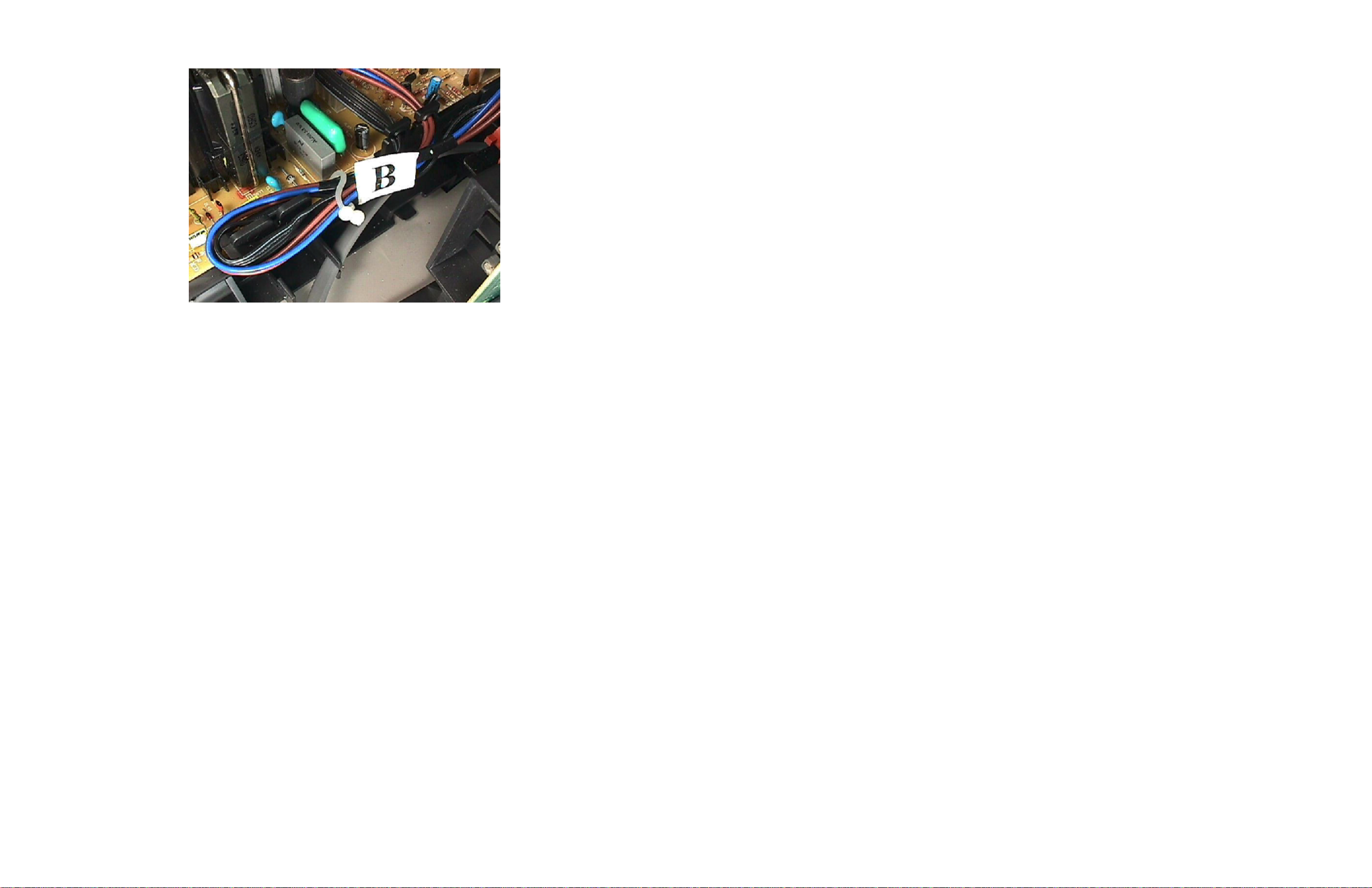
TX_TVD809 TX_TVD809
CABLE LEAD DRESS
E/W Module Lead Dress
PartList
Left Intentionally Blank
Page 5-5
Page 6-1
Page 8
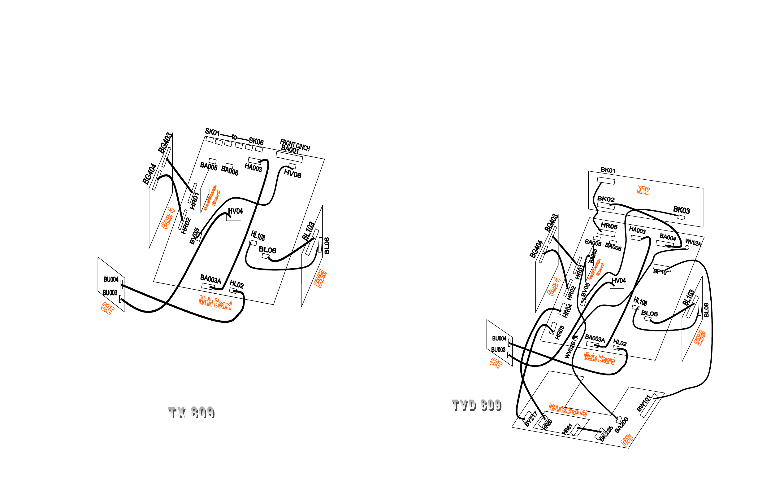
TX_TVD809 TX_TVD809
CHASSIS CONNECTION GUIDE
CHASSIS CONNECTION GUIDE
HR02-BG 404
__
PG
CC VIDEO
PWM(AUDIO)
IR_ C L K
IR_ D ATA
DVD_CMD_READY
RESET
EEPROM_W E
BURST
SR
IR/G LINK
DA TA_EVER
I²C
I²C CLK_EVER
+5VE
GND
HL02–BU004
+160V
HTR
HTR GND
GND
HV04–BU003
9VE
GND
B
G
R
GND
HR01 –B G 403
+5VE
R OSD
GND
G OSD
VSYNC
B OSD
HSYNC
FB OSD
IR IN
I²C CLK_EVER
FAULT
I²C DATA_EVER
SND-OGIC_A/D
SYNC DET
KEYDET2
KEYSEL 1
KEYSEL 2
ECO
KEYSEL 3
-> SPK R
BA005
BA006 -> SPK L
HV06 − BV05
GND
CINCH_VIDEO IN
HA 003 – HA003A
SPK L OUT
SPEAKER L
GND
SPK R OUT
SPEAKER R
BL06 – BL103
+24V/DG1
GND
UB/EWD
HR02-BG404
__
PG
CC VIDEO
PWM(AUDIO)
IR_CLK
IR_DATA
DVD_CMD_READY
RESET
EEPROM_WE
BURST
SR
IR/G LINK
I²C DATA_EVER
I²C CLK_EVER
+5VE
GND
BA200-BA003
DVD_L_Audio
GND
DVD_R_Audio
GND
HR80- HR04
+5VE
I2C_DATA_EVER
I2C_CLK_EVER
GND
IR CLK
GND
DVD CMD RDY
IR DA T A
HL02–BU004
+160V
HTR
HTR GND
GND
HV04–BU003
9VE
GND
B
G
R
GND
BY217-HR03
DVD_`C’
GND
DVD_`Y’
GND
N.C.
GND
HR01 – BG403
+5VE
R OSD
GND
G OSD
VSYNC
B OSD
HSYNC
FB OSD
IR IN
I²C CLK_EVER
FAULT
I²C DATA_EVER
SND-LOGIC_A/D
SYNC DET
KEYDET2
KEYSEL 1
KEYSEL 2
ECO
KEYSEL 3
BK03 − BV05
GND
CINCH_V IDEO IN
HR81 − BK225
GND
I2C_DATA_EVER
I2C_CLK_EVER
GND
IR_DVD
GND
DVD_ CMD_ RDY
NO CONTACT
BK02 – BA004
CINCH _AUD-IN L
GND
CINCH _AUD-IN R
SPK L OU T
SPK L
AUDIO − V
SPK R OUT
SPK R
BK01 – HR05
+5V
GND
N. C.
KEYSEL3
KEYDET2
KEYSEL2
KEYSEL1
POWER_ LED
IR IN
GND
BA005 -> SPK R
SPK L
BA006 ->
BP10 – BW101
12VE X2
8VS
CTRL
4VE X2
GND X 4
PG
-5VE
5VS
BL06 – BL103
+24V/DG1
GND
UB/EWD
BL08 – HL108
VPRBL
VRAMP
GND
FAULT
HA003 – HA003A
SPK L OUT
SPEAKER L
GND
SPK R OUT
SPEAKER R
BL08 – HL108
VPRBL
VRAMP
GND
FAULT
Page 5-2Page 5-1
Page 9
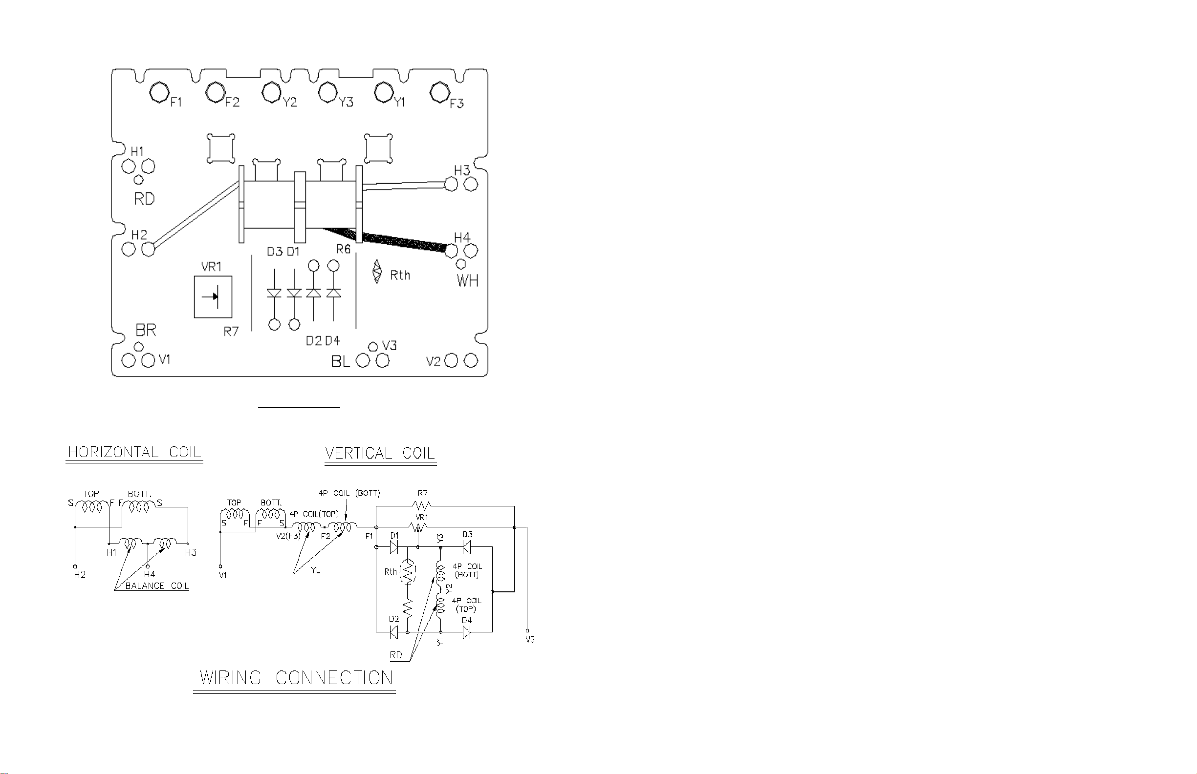
TX_TVD809 TX_TVD809
DEFLECTION YOKE
TER M INAL B L O C K
Left Intentionally Blank
Page 7-2Page 7-1
Page 10
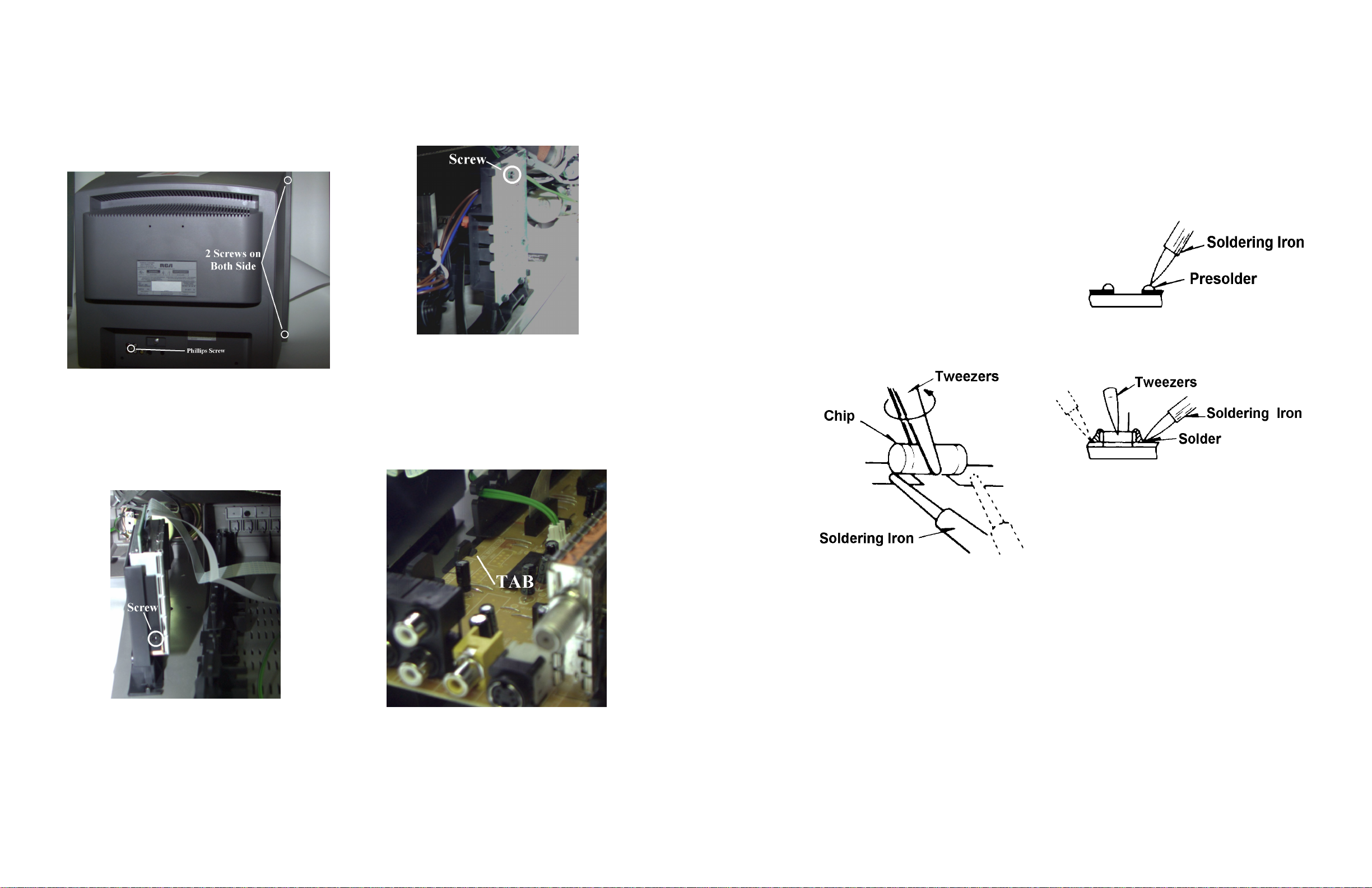
TX_TVD809 TX_TVD809
DISASSEMBLY PROCEDURES
Back Cover Removal
1. Remove five screws to release the back cover. 2
from each side and a small Phillips screw located
among the rear audio jacks.
2. Lift the back rear edge of the back cover and pull
back to remove.
3.
Gemstar Module Removal
1. Remove the back cover.
2. Remove the small screw at the lower back edge of
the plastic support.
3. Disconnect the 2 ribbon cables (BG403 & BG 404)
from the top of the Gemstar PCB.
4. Lift the Gemstar module straight up and out.
8. Raise the 2 tabs at the top of the plastic holder and
pull the top of the PCB clear of the tabs. Lift the
module strai ght up and out.
Main Chassis PCB Removal
9. Disconnect the AC power cable.
10. Remove the back cover.
11. Discharge the anode lead to the picture tube ground
strap and remove the anode lead before
disconnecting other cables.
12. Disconnect cable assemblies P1402, P3101, P3203,
P3401 and P4010 from the Main PCB.
CHIP COMPONENT REMOVAL
Replacement Procedure for Chip Removal
The following proced u re s are recom mended for the
replacement of the chip components used in this unit.
Failure to follow these procedures may lead to damage to
the copper traces and pads on the printed circuit boards.
1.Preparation for replacement
a. Soldering Iron: Use a pencil-type soldering iron
using less than 30 watts.
b. Solder Type: Eutectic Solder, Tin 63%/Lead
37%, is recommended.
c. Soldering Time: Do not apply heat for more than
4 seconds.
d. Preheating: Chip capacitors must be preheated
before installation. (130 degrees - 150 degrees
C).
Note: Chip component must not be reused after removal.
Excessive mechanical stress and rubbing of the
component electrode must be avoided.
2. Removing the chip component (Fig. 2-3):
Grasp the chip component body with tweezers and
alternately apply heat to both electrodes.
Note: Do not attempt to lift the component off the board
until the component is completely disconnected
from the board by a twisting action. A tte mp ting to
remove the component before it has completely
been disconnected can break the copper foil on
the printed circuit board.
3. Installing a c h ip component
a. Presolder the contact points on the circuit board
(Fig. 2-4).
Fig.2-4, Chip Component Presolder
b. Hold the component in position with tweezers and
solder the e lectrodes as shown (Fig.2-3).
Fig. 2-3 - Chip Component Installa tion
Note: Do not glue the replacement chip component to the
circuit board.
E/W Correction Module Removal
5. Remove the back cover.
6. Remove the small screw at the top center back of
the PCB.
7. Disconnect the 2 cables (BL108 & BL103) from the
E/W Correction PCB.
Figure 2-3, Removing Chip Components
When the solder on both electrodes has melted,
remove the chip component with a twisting motion.
13. Push out on the plastic Tabs on either side of the
tray and slide the chassis back and out until clear of
the
Page 2-2Page 2-1
Page 11
TX_TVD809 TX_TVD809
MODEL-TO-MAJOR ASSEMBLY CROSS REFERENCE
KEY TO MAJOR ASSEMBLIES
C1 Cinch Block Dummy (21120230)
D1 DVD Player
E1 E/W Correction (21120230)
G1 Gemstar (21146070)
CROSS REFERENCE
MODEL/
SERVICE NO. CHASSIS
BD20TF10 TVD809 D1, E1, G1, I1, K1, S1
F19426 TX809 C1, G1
F19436 TX809 C1, G1
F20TF10 TX809 C1, E1, G1, S1
MAJOR
ASSEMBLIES
I1 IR Interface (2112023A)
K1 KeyBoard ( 21120210)
S1 Sound Compressor (21120230)
SPECIFICATIONS (Subject to change without notice)
Power Input: 120 Volts AC 60Hz
Power Consumption: Maximum @ 120VAC
24 watts
Circuit Protection
Fusible Device Circuit Protected Physical Location
FP01 (2.5A, 250V) AC Input Power Supply PCB, Right Front Chassis
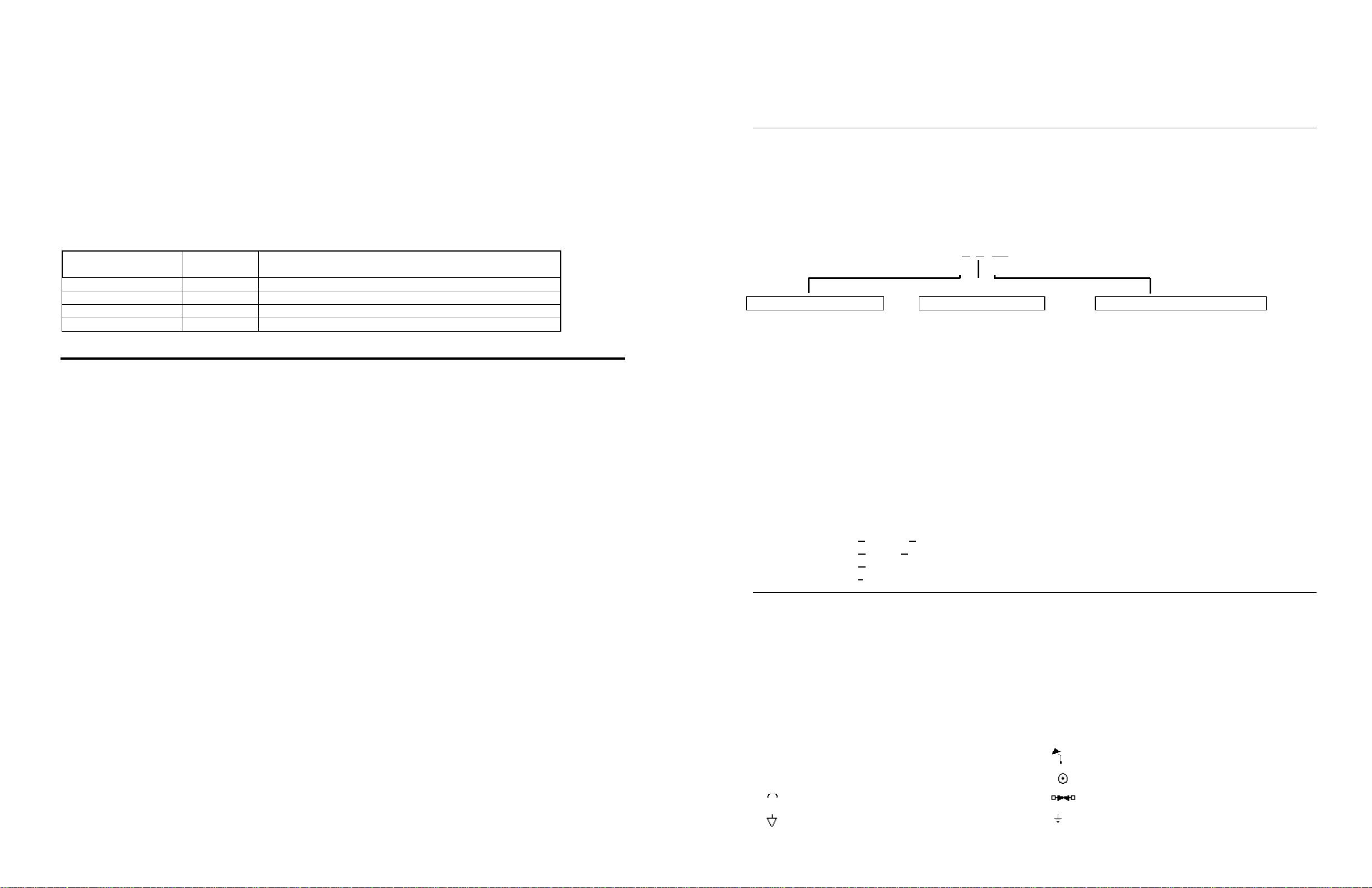
COMPONENT NUMBERING SYSTEM
Serviceability of this chassis is enhanced by road mapping on the top and bottom of the circuit boards. In addition
components are generally marked as to their circuit. The operation and features of the "TX" chassis is similar to the "CTC"
series chassis. However the component numbering system is slightly different than in the past. The component numbering for
the "TX" chassis reflects the component’s type and use as to the general circuit areas it is used. The component labeling
system is described below:
COMPONENT DESIGNATION: X X
COMPONENT TYPE CIRCUIT COMPONENT NUMBER
B - Connector A- Audio 01 - 099 Main PCB (top)
C - Capacitor C - Chroma 500 - 599 Main PCB (bottom)
D- Diode D- DC-DC Convertor
F - Fuse F - Vertical 101 - 199 E/W PCB
I-Integrated Circuit G-Gemstar
J - Jumper H - Tuner 001 - 099 Sound Compressor
L - Transformer/Inductor I - IF
P - Variable Resistor J - Sync Separator 401 - 599 Gemstar PCB
Q - Filter/Crystal K- Cu sto mer Contro l
R - Resistor L - Horizontal
S - Switch P - Power Supplies
T - Transistor R - System Control
V- Delay Line U- Kine Drivers 01 - 99 Kine PCB (top)
V- Video 500 - 599 Kine PCB (bottom)
Z- XRP
xxx
EXAMPLES:
TP20 - Transistor, P
RA543 - Resistor, Audio, 543 (number, bottom side of Main PCB)
CF07 - Capacitor, Vertical, 07 (number, top side of Main PCB)
IR501 _ Integrated Circuit, System Control, 501 (number, bottom side of Main PCB)
ower, 20 (number, top side of Main PCB)
SCHEMATIC NOTES
1. Resistor values are in ohms (R = 1, K = X1,000; Meg = X1,000,000). Tolerance i s 5%, unless otherwise specified.
Example: 1R5 = 1.5 ohm, 270R = 270 ohm, 2K7 = 2700 ohm, 1M5 = 1500000 ohm
2. Capacitor values 1.0 and above are in picofarads; values less than 1.0 are in µF, unless otherwise specified.
3. DC voltages measured with NTSC color bar signal applied (via RF channel 3), except for audio voltages, which are
measured with MTS stereo 1KHz signal applied. Voltages in parentheses ( ) indicate standby mode.
4. Waveforms measured with NTSC color bar signal applied (via RF channel 3), except for audio waveforms, which are
measured with MTS stereo 1KHz signal applied.
5. Special symbols:
< > indicates schematic zone locator
■ indicates wire-wrap stake indicates connection via point-to-point wire
indicates jumper wire (top side) indicates zero ohm chip (bottom side)
indicates "hot" ground indicates "cold" ground
indicates service test point
Page 1-4Page 1-3
Page 12
I2C2
IR In
ANT
Rear
Video
Y
C
Front
Vid
m
Tuner
Dat
Clk
Video
Input
Switch
CC
Vid
Gemstar
SysCon
C IG401
I2C1
EEPROM
IR01
Keyboard
Rear Audio In
WB
Audio
R
G
B
I2C2
Audio Mute
AC Degauss
VC
120VAC
L/R
Stereo Demux
Clk
I2C2
To
CRT
Vert Ouput
IF01
Horz Ouput
TL02
Stdby Power
Supply TP20
IV02
ClkDat
RGB
OSD
I
Y/C
2
C2
IF
Video
2
3
Bus Exp
IR501
Front Audio In
Sound/Pix IF
II60
Video/
Deflection
Processing
IV01
V-Out
Dat
Clk
H-Out
Dat
Clk
TX809 Simplified Block Diagram
2
& Tone/Vol
IA002
Dat
Int Spkr
Amp IA003
L/R
2
2
L/R
To
Vert
Yoke
Horz
Yoke
Audio
Compress
IA001
L/R
2
SysCon
IG401
L/R
To Int
Spkrs
2
L/R
2
Ext Spkr
Amp IA502
To
Head
Phones
Raw B+
IHVT
LL05
2
To Ext
Spkrs
L/R
Run
Supplies
TX809 Chassis Overview
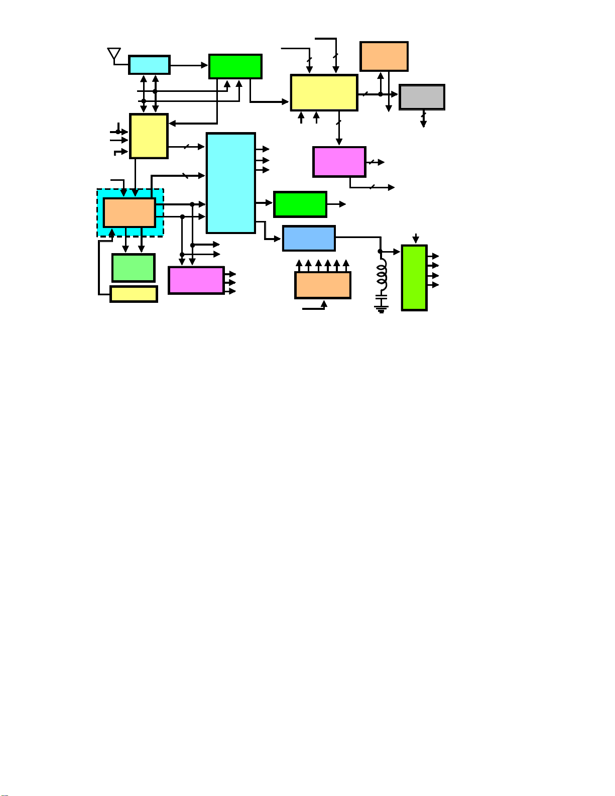
The TX809 is a conventional NTSC analog color television chassis that
incorporates many of the latest video features. The TX809 has both front and
rear composite video (CV) and audio inputs. The chassis also features a rear
Y/C (S-Video) input that provides maximum quality video reproduction. The
Sound/Pix IF IC (II60) provides the composite video signal. The video/deflection
processing IC (IV01) is responsible for final processing of the video signal. The
RGB OSD (on-screen-display) is also input to IV01 and overlaid onto the video
signal. IV01 also provides contrast, brightness, tint and color controls.
The TX809 system control microcomputer IG401 is located in the Gemstar
2
module and controls and monitors the operation of the instrument via two (2) I
C
buss. The I2C1 bus reads and writes operational data (customer and factory
settings, etc.) to and from the EEPROM, IR01. The second bus (I2C2) provides
control to all other areas of the chassis. The system control micro also monitors
the keyboard and decodes the IR input from the remote control. The I2C2 bus is
also applied to the bus expander IR501 where additional control signals for the
chassis is generated.
The Sound/Pix IF IC (II60) provides the wide band audio signal. The audio circuit
consists of four (4) major IC’s, they are the stereo Decoder/Demultiplexor IC
(IA002), an internal and external power amplifer IC’s (IA502 / IA003) and the
audio compressor (IA001). The Audio Compressor generates a control signal
that is fed back to the system control micro to limit severe and sudden unwanted
audio level changes.
Page 13
I2C2
IR In
ANT
Rear
Video
Y
C
Front
Vid
m
Tuner
Dat
Clk
Video
Input
Switch
IV02
CC
Vid
Gemstar
SysCon
C IG401
I2C1
EEPROM
IR01
Keyboard
Rear Audio In
To
Vert
Yoke
Horz
Yoke
Audio
Compress
IA001
L/R
2
SysCon
IG401
L/R
To Int
Spkrs
2
L/R
2
Ext Spkr
Amp IA502
To Ext
To
Head
Phones
Raw B+
IHVT
LL05
2
Spkrs
L/R
Run
Supplies
Front Audio In
Clk
R
To
G
CRT
B
Vert Ouput
IF01
Horz Ouput
L/R
2
Stereo Demux
& Tone/Vol
Dat
I2C2
TL02
Stdby Power
Supply TP20
IF
Video
2
Y/C
RGB
3
OSD
2
I
C2
ClkDat
Bus Exp
IR501
Sound/Pix IF
II60
Video/
Deflection
Processing
IV01
V-Out
Dat
Clk
H-Out
Dat
I2C2
Clk
Audio Mute
AC Degauss
VC
WB
Audio
L/R
2
IA002
2
L/R
Int Spkr
Amp IA003
120VAC
TX809 Simplified Block Diagram
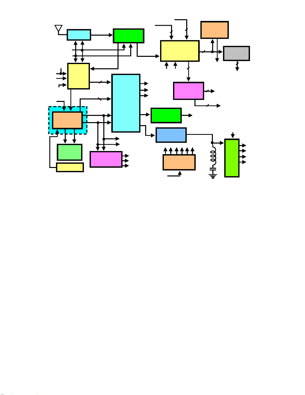
The standby power supply is a conventional switch mode power supply. The
standby supply is on whenever the instrument is plugged into 120VAC. The run
supplies are only on when the set is running and are generated via a
conventional horizontal scan-derived configuration. The voltages developed by
both the standby and run supplies can vary depending upon the model and it’s
features. The video/deflection processing IC (IV01) also generates both the
horizontal and vertical drive signals that are applied to the vertical and horizontal
drive circuits.
Page 14
TX_TVD809
11/03
TX_TVD809
TX_TVD809
F20TF10, F19425
Television
F19426, F19431, F19436
BD20TF10, 13V110TD
Basic Service Data
Technical Publications
P.O.Box 1976 / Indianapolis, Indiana 46206
SERVICE DATA INDEX
Page
Number
Electrical Alignment Procedures ...................................................................................... 3-1
Block Diagrams
Interconnect Diagram (TX809) ....................................................................................... 8-1
Interconnect Diagram (TVD809) .................................................................................... 8-2
Circuit Boards.................................................................................................................... 10-1
Disassembly
Instrument Disassembly .................................................................................................. 2-1
Component Removal ....................................................................................................... 2-2
General Information
Model to Major Assembly Cross Reference .................................................................... 1-3
Safety Precautions ........................................................................................................... 1-2
Schematic Notes .............................................................................................................. 1-4
Specifications .................................................................................................................. 1-3
Schematic Diagrams
Power Supply .................................................................................................................. 9-1
Deflection ........................................................................................................................ 9-2
System Control ................................................................................................................ 9-3
Gemstar ........................................................................................................................... 9-4
uP Controller (F19425, F19431) ..................................................................................... 9-5
Tuner ............................................................................................................................... 9-6
Video ............................................................................................................................... 9-7
Kine Driver...................................................................................................................... 9-8
Kine Driver (F19425, F19431)........................................................................................ 9-9
DVD (Connectors) .......................................................................................................... 9-10
Keyboard/FAV (20V)...................................................................................................... 9-11
Keyboard/FAV (13V)...................................................................................................... 9-12
Audio (IF, TVB) (BD20TF10) ........................................................................................ 9-13
Audio (Output) (BD20TF10) .......................................................................................... 9-14
Audio (IF, TVB) (13V110TD) ........................................................................................ 9-15
Audio (Output) (13V110TD) .......................................................................................... 9-16
Audio (IF, TVB) (F20TF10, F19436, F19431) ............................................................... 9-17
Audio (Output) (F20TF10, F19436, F19431) ................................................................. 9-18
Audio (F19426) .............................................................................................................. 9-19
Audio (F19425) .............................................................................................................. 9-20
Troubleshooting Aids
Connection Guide............................................................................................................ 5-1
Lead Dress ....................................................................................................................... 5-3
Voltage Charts................................................................................................................. 5A-1
Yoke Wiring Diagram ..................................................................................................... 7-1
SAFETY NOTICE
USE ISOLATION TRANSFORMER WHEN SERVICING
Components having special safety characteristics are identified by a ( ) on schematics and on the parts list in this Service Data and its bulletins. Before
servicing this instrument, it is important that the service technician read and follow the “Safety Precautions” in the Basic Service Data.
SAFETY PRECAUTIONS
DO NOT OPERATE THIS INSTRUMENT OR PERMIT IT TO BE OPERATED WITHOUT ALL PROTECTIVE DEVICES INSTALLED AND
FUNCTIONING. SERVICERS WHO DEFEAT SAFETY FEATURES OR
FAIL TO PERFORM SAFETY CHECKS MAY BE LIABLE FOR ANY
RESULTING DAMAGE, AND MAY EXPOSE THEMSELVES AND OTHERS TO POSSIBLE INJURY.
READ AND COMPLY WITH ALL CAUTION AND SAFETY-RELATED
NOTES ON OR INSIDE THE RECEIVER CABINET, AND THE RECEIVER CHASSIS, OR ON THE PICTURE TUBE.
SAFETY GLASSES SHOULD BE USED WHEN SERVICING ELECTRONIC INSTRUMENTS. INADVERTENTLY OVERSTRESSING COMPONENTS MAY CAUSE THEM TO SHATTER, DISCHARGING SMALL
PARTICLES.
DESIGN ALTERATION WARNING - Do n
electrical design of this TV receiver. Design alterations and additions may alter
the safety characteristics of this receiver and create a hazard to the user. Design
alterations or additions may void the manufacturer’s warranty and may make you,
the servicer, responsible for personal injury or property damage resulting therefrom.
BEFORE RETURNING AN INSTRUMENT TO THE CUSTOMER, always
make a safety check of the entire instrument, including, but not limited to, the
following items:
FIRE AND SHOCK HAZARD
1. Never release a repaired unit unless all protective devices such as insulators, barriers, covers, strain reliefs and other protective hardware have been
installed in accordance with the original design.
2. Be sure that there are no cabinet openings through which an adult or a child
might be able to insert their fingers and contact a hazardous voltage. Such
openings include, but are not limited to: (a) spacing between picture tube
and cabinet mask, (b) excessively wide cabinet ventilation slots, and (c) an
improperly fitted or incorrectly secured back cover.
3. Observe original lead dress. Take care to restore leads to their original
dress. Make sure that leads are not in contact with sharp edges or thermally
hot parts. Always inspect in all areas for pinched, out-of-place or frayed
wiring. Do not change spacing between adjacent components, or between
components and printed circuit board. Check the AC power cord for damage.
4. Be certain to remove loose solder balls and all other loose foreign particles.
5. Check components, parts and/or wiring for physical evidence of damage,
overheating or deterioration, and replace if necessary. Determine the cause
of damage and/or overheating and, if necessary, take corrective action to
remove any potential safety hazard.
6. Parts Replacement - Many TV electrical and mechanical parts have special
safety-related characteristics, some of which are often not evident from visual inspection, and the protection they give cannot necessarily be obtained
by replacing them with components rated for higher voltage, wattage, etc.
Parts that have special safety characteristics are identified in this service
data by a ( ) on schematics and in the parts list. Use of a substitute
replacement that does not have the same safety characteristics as the recommended replacement part in the service data parts list may create shock, fire
and/or other hazards. Always consult the appropriate current service literature for the latest information.
7. Some TV receiver chassis’ normally have 85VAC (RMS) between chassis
and earth ground, regardless of the AC plug polarity. Some TV receiver
chassis’ are electrically connected directly to one conductor of the AC power
cord. Some TV receiver chassis’ have a secondary ground system in addition to the main chassis ground. This secondary ground system is not isolated from the AC power line. The two ground systems are electrically
separated by insulating material that must not be defeated or altered. Thus,
when servicing any unit always use a separate isolation transformer for the
chassis. Failure to use a separate isolation transformer may expose the
servicer to possible shock hazard, and may cause damage to servicing instruments.
8. Many electronic products use a polarized AC line cord (one wide pin on the
plug). Defeating this safety feature may create a potential hazard to the
servicer and the user. Extension cords that do not incorporate the polarizing
feature should never be used.
PICTURE TUBE IMPLOSION WARNING - The picture tube in this
receiver employs integral implosion protection. For continued implosion protection,
replace the picture tube only with one of the same type number.
ot alter or add to the mechanical or
Do not remove, install, or otherwise handle the picture tube in any manner without first putting on shatterproof goggles equipped with side shields. People not so
equipped must be kept safely away while picture tubes are handled. Keep the
picture tube away from your body. Do not handle the picture tube by its neck.
Some “in-line” picture tubes are equipped with a permanently attached deflection
yoke; because of potential hazard, do not try to remove such “permanently attached” yokes from the picture tube.
X-RADIATION AND HIGH VOLTAGE LIMITS - Because the picture
tube is the primary source of X-radiation in solid-state TV receivers, it is specially
constructed to prohibit X-radiation emissions. For continued X-radiation protection, a replacement picture tube must be the same type as the original. The picture
shields, mounting hardware and lenses (projection TV) may also perform an Xradiation protection function, and they must be correctly in place. Anode connectors contain an X-radiation shield - use only the manufacturer’s specified anode
connectors. High voltage must be measured each time servicing that involves
power supply, horizontal deflection or high voltage circuits is performed. Correct
operation of the X-radiation circuits must also be confirmed each time these circuits are serviced (X-radiation circuits may also be called “horizontal disable” or
“hold-down” circuits). Read and apply high voltage limits and, if the chassis is so
equipped, the X-radiation protection circuit specifications. These limits and specifications are given on instrument labels and are included in this service data. High
voltage is maintained within specified limits by close-tolerance safety-related components (and adjustments) in the high voltage circuit. If high voltage exceeds
specified limits, check each safety related component specified on the schematic
and take corrective action.
ANTENNA LEAKAGE RESISTANCE CHECK - With the instrument AC
plug removed from the AC source, connect an electrical jumper across the two AC
plug prongs. Place the instrument AC switch (if applicable) in the “on” position.
Connect one lead of an ohmmeter to the AC plug prongs and touch the other
ohmmeter lead, in turn, to each (exposed) antenna input terminal screw and/or
coaxial connector. If the measured resistance is less than 1.0 Megohm, or greater
than 5.2 Megohm, an abnormality exists which must be corrected before the instrument is returned to the customer. Repeat this test with the AC switch in the
“off” position.
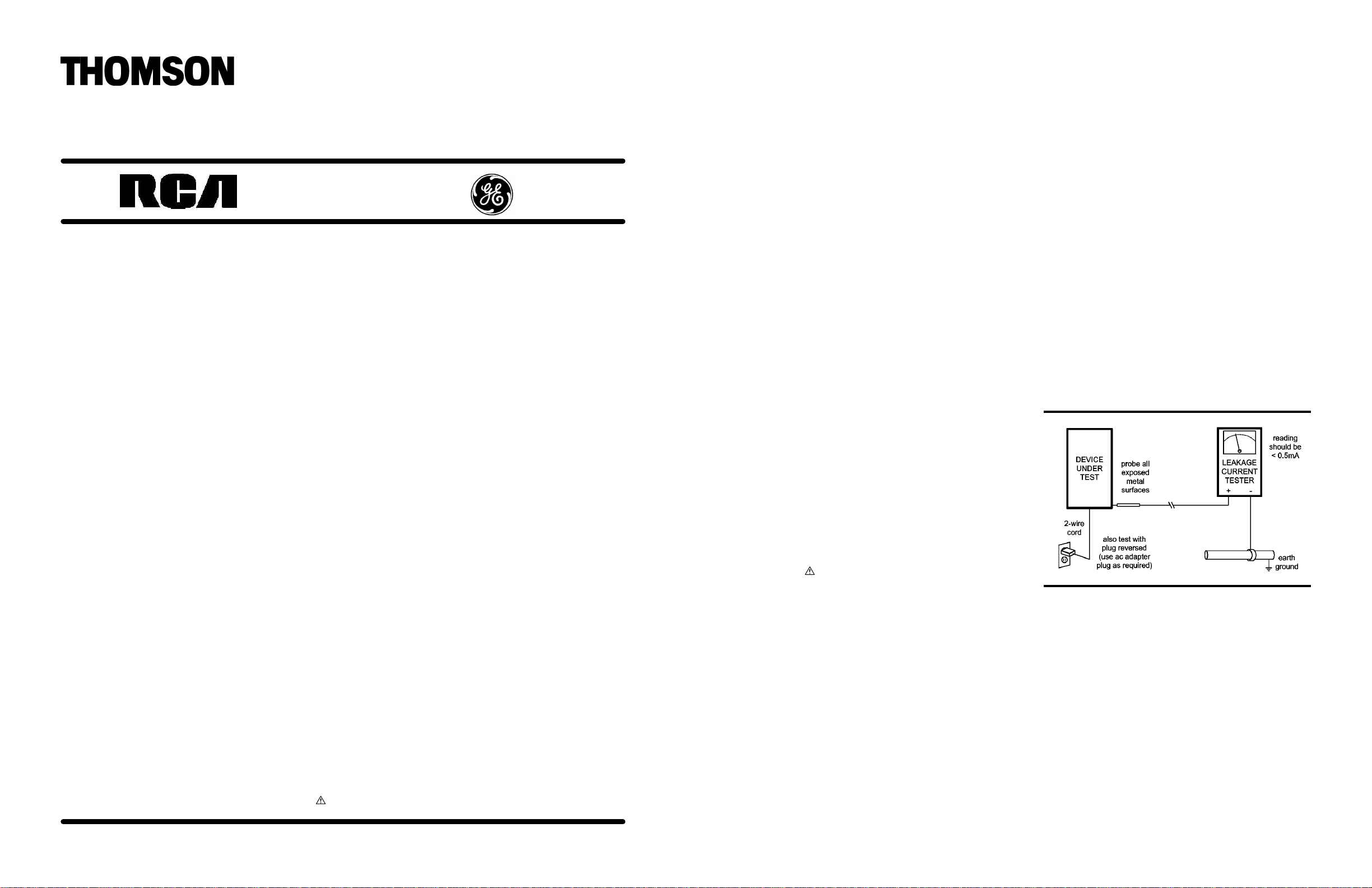
LEAKAGE CURRENT HOT CHECK FOR 2-WIRE OR 3-WIRE
GROUNDED CORD SETS - With the instrument completely reassembled,
plug the AC line cord into the mains AC outlet at normal line voltage via a nonpolarized adapter. DO NOT GROUND THE 3RD PRONG OF THE ADAPTER
AND DO NOT USE AN ISOLATION TRANSFORMER. Use a leakage current
tester or metering system that complies with American National Standards Institute (ANSI) C101.1 Leakage Current for Appliances and with Underwriters Laboratories (UL) 1492 (Section 67). With the instrument AC switch first in the “on”
position and then in the “off” position, measure from a known earth ground (metal
water pipe, conduit, etc.) to all exposed metal parts of the instrument (antennas,
handle bracket, metal cabinet, screwheads, metallic overlays, control shafts, etc.).
Any current measured must not exceed 0.5 milliampere. Reverse the adapter plug
in the outlet and repeat the test. ANY MEASUREMENTS NOT WITHIN THE
LIMITS SPECIFIED HEREIN INDICATE A POTENTIAL SHOCK HAZARD THAT MUST BE ELIMINATED BEFORE RETURNING THE INSTRUMENT TO THE CUSTOMER OR BEFORE CONNECTING THE
ANTENNA OR ACCESSORIES. If a leakage current tester is not available,
connect a 1.5 Kohm, 10 Watt resistor, in parallel with a 0.15 µF, 150V capacitor,
between earth ground and each exposed metal part of the instrument (as shown
above). Use an AC voltmeter with at least 5000 ohm/volt sensitivity to measure
the potential across the resistor. The potential measured for any exposed metal
surface must not exceed 0.75 volts.
First Edition - First Printing
Copyright 2003 - Thomson Consumer Electronics, Inc.
Printed in U.S.A. - Trademark(s)® Registered - Marca(s) Registrada(s)
AD00001103
TX_TVD809
Page 1-2
Page 15
Rear
Video
Y
C
Front
(CV)
Video
CC Video
to SysCon
IG401
(CV)
ANT
I2C2
Dat
Clk
6
5
10
15
Tuner
42
Video
Input
Switch
IV02
Y-In
20 11
C-In
7
Y-Out
17
C-Out
16
18
Chroma
Buff/Filter
IF
Video
TV523
Sound/Pix IF
1/2
(CV)
Video
2
I
C2
10
11
II60
17
(CV)
Luma
Buff/Filter
TV522/526
DatClk
Deflection
43
Processing
45
OSD
from SysCon
IG401
16 17
15
Video/
IV01
Dat
Clk
19
20
21
28
27
To
CRT
R
G
B
2
I
C2
TX809 Video Switching/Processing Block Diagram
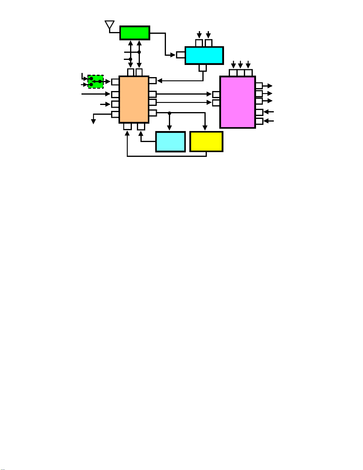
Video Switching & Processing
The Video Switching and Processing circuitry in the TX809 includes the Video
Input Switch IV02, the Video/Deflection Processing IC IV01, the Sound/Pix IF IC
II60 and the tuner. The video switch IV02, video/deflection IC IV01 processor
and the sound/pix IC II60 are controlled via the System Control IG401. The CC
Video (Closed Caption) is output from pin 15 of switch IV02 and sent to the
system control (IG401) for decoding. Transistors TV522, TV523 and TV526 are
used to separate the composite video signals into separate luma (Y) and chroma
(C) signals. The composite video (CV) from the Sound/Pix IF (II60) and the front
and rear input jacks are first routed through IV02 and output at pin 18. The
composite video is applied to chroma and luma filter circuits for separation. The
separated Y & C are then input back into IV01 at pins 11 and 20. The Y/C (SVideo) input is routed directly through switch IV02 for final processing. The
selected video is output at pin 16 and 17 and applied to pins 43 and 45 of IV01
for final processing. All brightness, contrast, color and tint adjustments are
performed by the video processor (IV01). The RGB OSD (On-Screen-Display)
from the system control IG401 is also input to the video processor at pins 15, 16
& 17.
Troubleshooting
NOTE: Always use known video source such as color bars. If a video problem
is suspected perform the following:
1. Confirm presence of all power supplies for circuit.
2. Check I2C2 for data & clock activity when a function is selected.
3. Check for video from II60-17 (Sound/Pix IF) during tuner operation.
4. Apply video to front/rear video inputs and check for video at IV01-18.
5. If OK, check for Y & C out of transistors TV522, TV523 & TV526.
6. If OK, check for Y & C at IV02-16/17.
7. Check for correct RGB out of IV01-19/20/21 (Video Processor).
Page 16
TX_TVD809 TX_TVD809
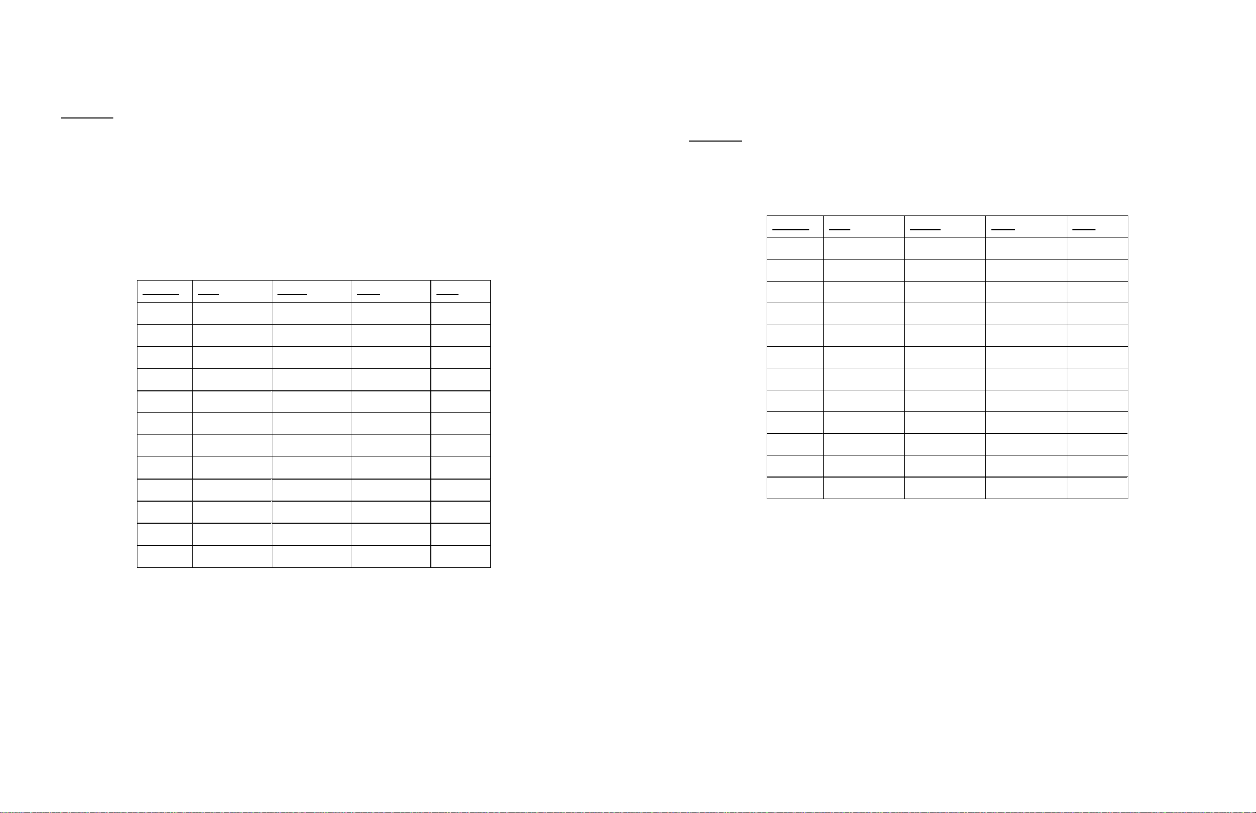
Voltage Chart (Power Supply)
Voltage Chart (Power Supply)
FROSIN Power Supply Outpu t Voltages
Cond it ions
TV on: Picture Color Bar
Brightness - 50%
Conditions
DVD on: Play
Color - 50%
Contrast - 50%
Volume - 1/8 Sound power.
TV ON mode
Supply Min Norm Max Unit
UB 114 115 116 VDC
UA 11 11.5 12 VDC
14V 12.0 13.0 14.5 V D C
12VE 11.0 12.2 14 VDC
9VE 8.5 8.9 9.5 VDC
9VS 8.5 8.9 9.5 VDC
9VS2 8.5 8.9 9.5 VDC
8VS 7.5 8.1 8.5 VDC
+5VE 4.85 5.1 5.35 VDC
DVD ON mode
Supply Min Norm Max Unit
UB 114 115 116 VDC
UA 11 11.5 12 VDC
14V 12.0 13.0 14.5 VDC
12VE 11.0 12.2 14 VDC
9VE 8.5 8.9 9.5 VDC
9VS 8.5 8.9 9.5 VDC
9VS2 8.5 8.9 9.5 VDC
8VS 7.5 8.1 8.5 VDC
+5VE 4.85 5.1 5.35 VDC
-5VE -5 -5.4 -6 VDC
5VS 4.85 5.5 6 VDC
4VE 4 5.5 6 VDC
-5VE -5 -5.4 -6 VDC
5VS 4.85 5.5 6 VDC
4VE 4 5.5 6 VDC
Page 5A-2Page 5A-1
Page 17
TX_TVD809 TX_TVD809
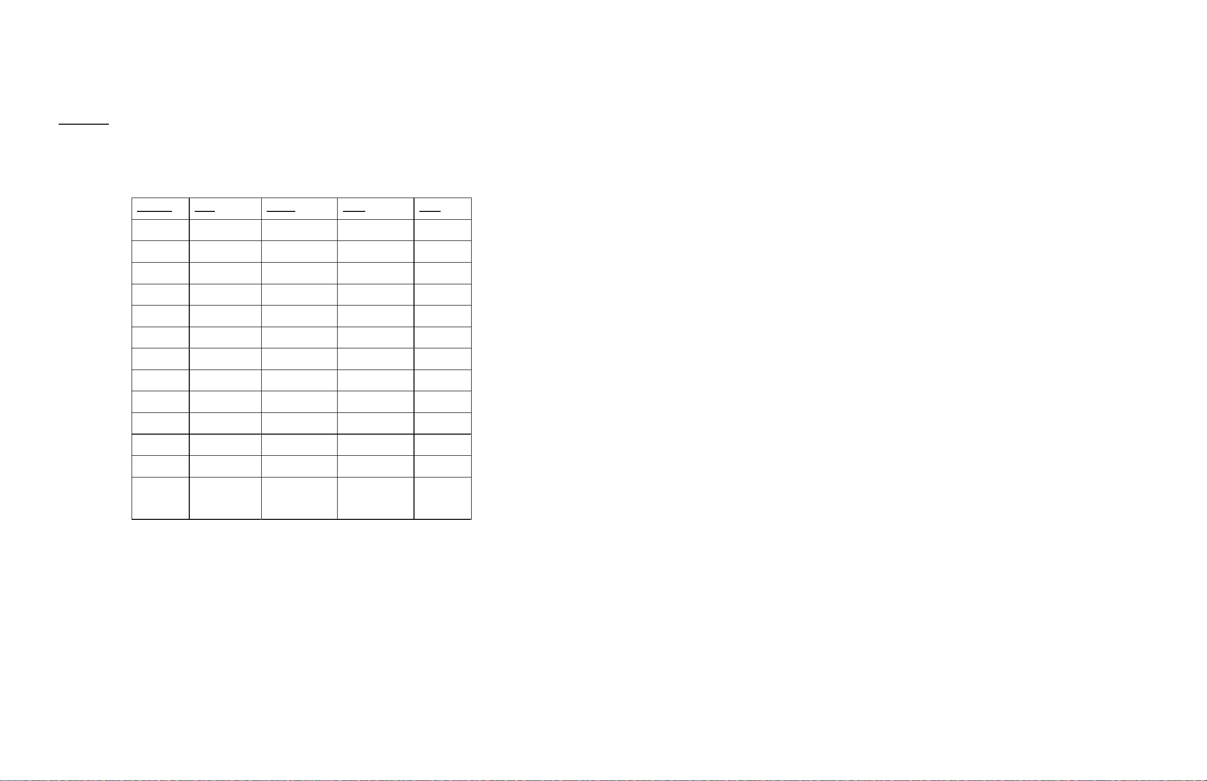
Voltage Chart (Power Supply)
Con ditions
Voltage Chart (Power Supply)
TV OFF (AC connected):
Standby mode
Supply Min Norm Max Unit
UB 134 135 136.5 VDC
UA 18 18.5 19 VDC
14V 13.5 14.3 14.7 V DC
12VE 11.7 12.2 12.7 VD C
9VE 8.5 8.9 9.5 VDC
9VS --- --- --- VD C
9VS2 --- --- --- VDC
8VS --- --- --- VD C
+5VE 4.85 5.1 5.35 VDC
-5VE -5 -5.3 -6 VDC
5VS --- --- --- VD C
4VE 7.3 7.8 8.3 VDC
Standby
11 12.5 13 Watts
Power
Left Intentionally Blank
Page 5A-3
Page 5A-4
Page 18
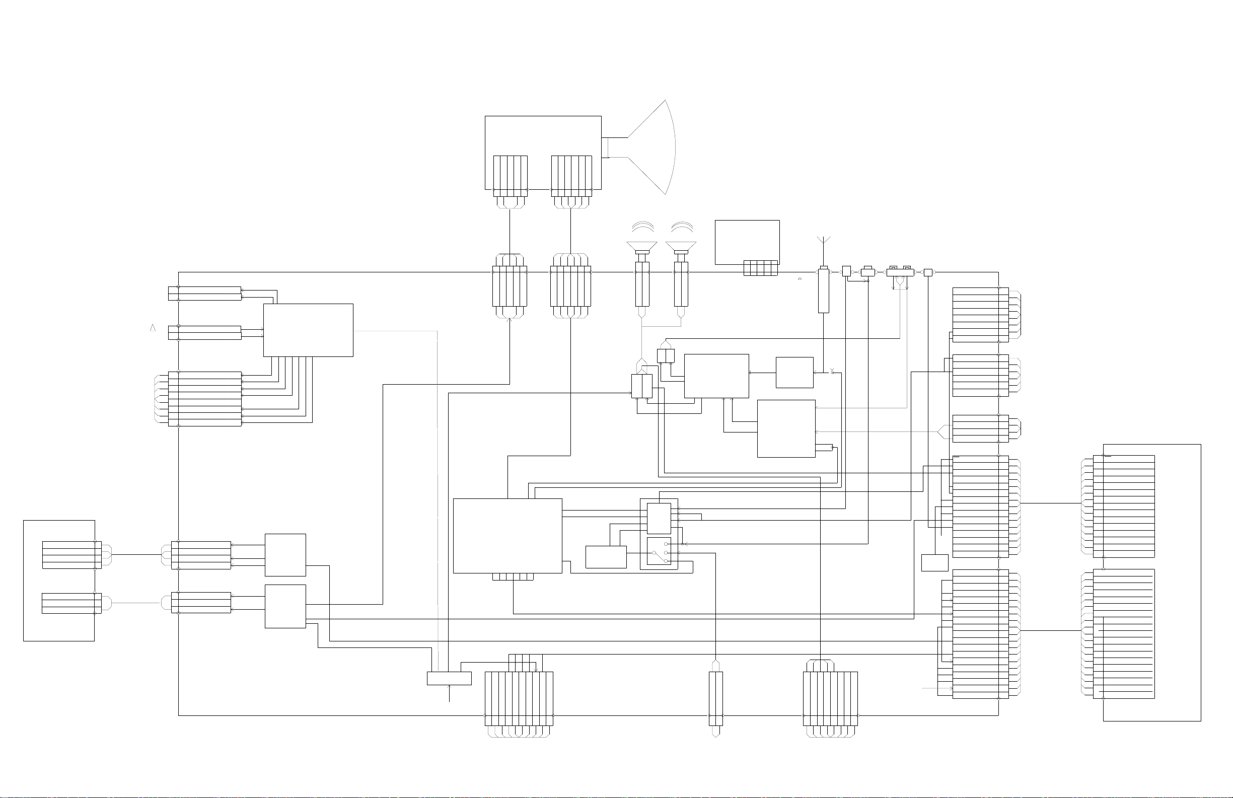
TX809
EWM BOARD
Part of 2112023_
HL108
VPRBL
VRAMP
GND
FAULT
BL103
DG1/+24V
GND
UB/E/WD
Interconnect Drawing
Part of 2112023_
CRT BOARD
IA003
POWER
AMP
CY
CRT
1
2
BA006
SPEAKER_L
GND
IV02
17
16
SWITCH
20
11
VIDEO
SWITCH
18
Part of 2112023_
SPK RSPK L
1
2
BA005
SPEAKER_R
GND
IS100
PREAMP
PWM
CC VIDEO
15
Y/C
3
1
5
6
6
10
8
DVD_Y
DVD_C
AV_CHROMA
REAR VIDEO
FRONT VIDEO
RF VIDEORF VIDEO
Sound Compressor PCB
BA001
654321
BA008
IS001 SOUND IF
UPC1851
FVIDEO_IN
GND
1
PS001
IS002
MC1452
AUDIO SWITCH
BA004BV05
ANT
BV01
TUNER
REAR_L/R
DVD_L/R
RF MONO
FRONT L
TO HORIZONTAL
DEFLECTION
L_OUT
L_IN
AUDIO_GND
R_IN
R_OUT
876543221
S-VHS VIDEO
AUDIO_R_IN
AUDIO_L_IN
GND
REAR
AUDIO_CLINCH
RL
TO POWER SUPPLY
FROM HOR DEF
TO POWER SUPPLY
G-LINK
IR01
EEPROM
TO HR03
IN/OUT
BG01BV02 P11
HR04
+5VE
SDA
SCL
GND
IR_DVD
GND
DVD_CMD_RDY
IR_DATA
HR03
DVD_C
GND
DVD_Y
GND
GND
BA002
GND
DVD_R
GND
DVD_L
HR02
PG
CC_VIDEO
PWM(AUDIO)
IR_CLK
IR_DATA
DVD_CMD_READY
RESET
EEPROM_WE
BURST
SR
IR/G LINK
IIC DATA EVER
IIC CLOCK EVER
+5VE
GND
HR01
+5VE
R_OSD
GND
G_OSD
VSYNC
B_OSD
HSYNC
FB_OSD
IR IN
IIC_CLK_EVER2
FAULT
IIC_DATA_EVER2
SND_LOGIC_A/D
SYNC_DET
KEYDET 2
KEYSEL1
KEYSEL2
ECO ON/STANDBY
KEYSEL3
1
2
3
4
5
6
7
8
1
2
3
4
5
6
1
2
3
4
1
2
3
4
5
6
7
8
9
10
11
12
13
14
15
1
2
3
4
5
6
7
8
9
10
11
12
13
14
15
16
17
18
19
GEM STAR 4
HR02
PG
1
CC_VIDEO
2
PWM(AUDIO)
3
IR_CLK
4
IR_DATA
5
DVD_CMD_READY
6
RESET
7
EEPROM_WE
8
BURST
9
SR
10
IR/G LINK
11
IIC DATA EVER
12
IIC CLOCK EVER
13
+5VE
14
15
GND
HR01
+5VE
1
R_OSD
2
GND
3
G_OSD
4
VSYNC
5
B_OSD
6
HSYNC
7
FB_OSD
8
IR IN
9
IIC_CLK_EVER2
10
FAULT
11
IIC_DATA_EVER2
12
SND_LOGIC_A/D
13
SYNC_DET
14
KEYDET 2
15
KEYSEL1
16
KEYSEL2
17
ECO ON/STANDBY
18
KEYSEL3
19
PCB 2114607_
BU04BU03
CRT_GND
110 AC POWER
!
1
2
1
2
BP02
AC DEGAUSS1
AC DEGAUSS2
BP01
AC1
AC2
PCB 21116590_
POWER SUPPY SECTION
AC/DC_DEGAUSS
1
GND
2
GND
HTR GND
HTR
HTR GND
HTR
+160V
+160V
CRT_GND
1
9VE
GND
9VE
BGR
655 44 33 22 11
65544332
HV04HL02
RGB
GND
HP01
12VE
1
8VE
2
5VS
3
4VE
4
GND X 4
5
PG
6
-5VE
7
5VS
8
TV MAIN BOARD
IV01
BPL08
1
2
3
4
1
FAULT
2
GND
3
VRAMP
4
VPRBL
VERTICAL
DEFLECTION
VIDEO IC
TA1268
RF MONO
VIDEO IF
VIDEO
CHROMA
AUDIO_MUTE
EQUALISING
CCT & CHROMA
BPF/COMB FILTER
TEA6415C
BPL06
1
2
3
1
2
3
HORIZONTAL
DEFLECTION
IR501
BUS EXPANDER
KEYSEL3
A/D
POWER_LED
IR
GND
KEYSEL1
KEYSEL2
GND
+5V
10
9
8
3
4
5
6
7
BS003
1
2
PAGE 8-1
PAGE 8-1
Page 19
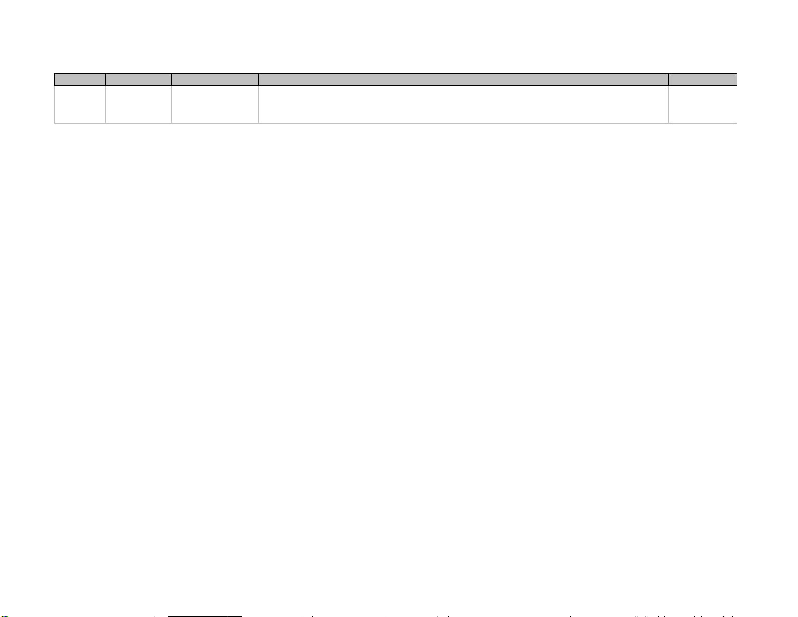
Chassis Part Symbol Defective Circuit Symptom solution
No audio and the dvd is inoperative, the door won't even open. The unit appears to be in
the dvd lock mode. The DVD unit was found to be at fault. Replacing the dvd unit restored
TVD809 Mech_DVD Mechanical
normal operation. (This was the latest version of the dvd.) Replace DVD
 Loading...